Note: Descriptions are shown in the official language in which they were submitted.
CA 02262124 1999-02-16
PRIORITY APPLICATION 0378/98
SWITZERLAND
EMP - CHARGE ELIMINATOR
This invention concerns a EMP-charge eliminator device for a
co-axial electric cable consisting of a Iamda/4 line,
connected to a housing joining the external conductor and
also to the internal conductor of the co-axial cable, at the
end of which there is an charge eliminator component
connected to the housing according to the definitions given
in the claims.
Artificially created electromagnetic impulses, as may be
produced by motors, switches, phased or oscillating circuits
or similar, as well as those caused naturally from direct or
indirect lightening strikes, are transmitted by means of
inductive, capacitative or galvanic connectors through
co-axial cables and may damage or even destroy electrical
equipment connected to these lines. It is common practice
to protect such equipment, at the input point, against
substantial voltage overloads, interferance voltages or
lightening surges by means of devices which eliminate or
deflect these impulses. For example, there are
EMP-Gas-Eliminators also called EMP Charge Eliminators, with
which such damaging currents, voltages and certain
frequencies may be eliminated or deflected. Such circuits
CA 02262124 1999-02-16
page 2
are described in Swiss Patent CH-660261 and Swiss Patent
Applications 914/95 and 158/97.
The Swiss Patent Application 158/97 provides that
interfering currents and voltages are eliminated or
deflected by means of a gas discharge voltage overload
eliminator which is located between and connects the
external conductor of the co-axial cable and the lamda/2
line. This Iamda/2 line with its resonant cavity and the
gas discharge voltage overload eliminator connected in
series, acts as a filter sensitive to frequencies over a
number of frequency bands, which is also able to
simultaneously transmit AC/DC supply voltages.
The presently known protective circuits with gas discharge
voltage overload eliminators exhibit a number of
disadvantages, such as the generation of intermodulation
products during the transmission of HF capacity. The HF
capacity generates a certain pre-ionisation which cause
lower reset characteristics in the gas discharge voltage
overload eliminators. Furthermore, the static response
voltage of the gas discharge voltage overload eliminators is
dependent on the HF transmission capacity. These
disadvantages limit the application of the such gas
discharge eliminators for branched circuits.
CA 02262124 1999-02-16
page 3
It is the object of this invention to create an EMP-charge
eliminator which does not generate intermodulation products
during HF capacity transmission, which does not show a
decline in reset characteristics, which is independent of
the chosen transmission capacity and which is fitted with a
voltage overload eliminator of the smallest possible
response voltage and which, at the same time, allows the
transmission of AC/DC supply voltages.
These objectives are achieved by the claims which define
this invention.
The EMP-charge eliminator device according to Claim 1
incorporates an charge eliminator component, interchangibly
inserted, in parallel, between the housing and a
electrically extended lamda/4 line and a capacitor. This
charge eliminator component connects the conductor for the
HF with the housing and forms a parallel oscilatory circuit
with the lamda/4 line. Gas discharge voltage overload
eliminators, Varistors (variable resistors) and well as
different types of diodes are all suitable as voltage
overload eliminator components.
Such a circuit enables the transmission of AC/DC supply
voltages and is also suited for the ,simultaneous
transmission of HF frequency bands of high capacity without
the generation of intermodulation products or that the reset
CA 02262124 2000-04-12
29718-3
4
characteristics decrease when a gas discharge voltage overload
eliminator is used. Furthermore, such an arrangement of the
circuit enables the transmission of high HF capacities, this in
broad frequency bands, at very high, and in principle maximally
unlimited, frequencies and with the smallest possible response
voltage of the voltage overload eliminator. With this
invention, appliances may be supplied with AC/DC power at the
same time effectively protected from damaging current surges.
In accordance with one aspect of the invention three
is provided a de-coupled EMP-charge eliminator device for use
in a co-axial cable, said device including a first conductor
for connecting inner conductor portions of said co-axial cable,
a second conductor connected to said first conductor, a charge
eliminator having a first terminal thereof electrically
connected to said second conductor, a housing connected to a
second terminal of said charge eliminator and adopted to be
connected to outer conductor portions of said co-axial cable,
characterized by a concentrated capacitor connected between
said second conductor and said housing in parallel with said
charge eliminator forming a HF-short circuit breaker, via the
capacitor, and said conductor forming a lamda/4 short circuit
conductor for the frequency band to be transmitted.
Some preferred embodiments of this invention are
described in the following:
Fig. 1 shows, in principle, an electric circuit of
the first preferred embodiment of a de-coupled EMP-charge
eliminator device with a gas discharge voltage overload
eliminator as the charge eliminator component,
Fig. 2 shows, by way of example, a cross-sectional
view through a part of the first preferred embodiment of the
EMP-charge eliminator device according to Fig. 1,
CA 02262124 2000-04-12
29718-3
4a
Fig. 3 shows, in principle, an electric circuit of a
further preferred embodiment of a de-coupled EMP-charge
eliminator device with a Varistor as the charge eliminator
component,
CA 02262124 1999-02-16
page 5
Fig.4 shows, in principle, a electic circuit of a further
preferred embodiment of an de-coupled EMP-charge
eliminator device with a diode as the charge
eliminator component,
Fig.5 shows, in principle, a electic circuit of a further
preferred embodiment of an de-coupled EMP-charge
eliminator device with differing conductor segments
along the main electrical conductor.
Fig.6 shows, by way of example, a cross-sectional view
through a part of a further preferred embodiment of
the EMP-charge eliminator device according to Fig.5.
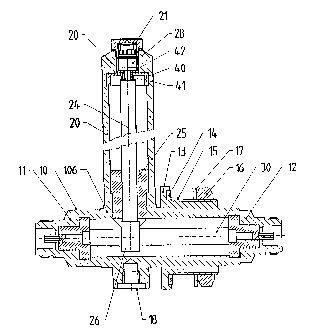
By way of example, the EMP-charge eliminator device, created
as a plug-in device, and according to the cross-sectional
view depicted in Fig.2 or 6, it consists of a external
conductor 10 in the form of a cylindrical housing with
couplings 11 and 12 at both ends as screw or plug connectors
for co-axial electical conductors. The coupling 11, to the
left in the drawing, is designed as the connection to the
unprotected side, while coupling 12, to the right in the
drawing, is designed as the protected connection to the
electronic appliance. In the way depicted in these
embodiments of the EMP-charge eliminator device, an earth
connection is intended by means of a screw coupling or by
CA 02262124 1999-02-16
page 6
means of an duct in the housing. For this purpose, a screw
coupling 18 or a flange 13 is provided on the housing 10.
The flange together with a washer 17 or similar and with a
nut 16 provides a screw connection to the housing wall. An
additional seal or packing 14 of refined soft copper serves
as a low resistance contact of poor inductivity. Other
possibilities of forming such connections may be created by
technically competent persons in relation to this
invention.
An external hollow cylinder is screwed into or fixed onto a
central section 106 of the external conductor 10. This
external hollow cylinder 20 has an end-cap 21 screwed onto
it. The charge eliminator component 28 is inserted into
this end-cap 21. A number of designs of charge eliminator
components 28 are possible. The charge eliminator component
28 may be in the form of a gas discharge voltage overload
eliminator (see Fig.l and 2), or also in the form of a
Varistor (see Fig. 3), or in the form of a diode, eg.
Transzorb Diode, Zener Diode, suppressor diode, protective
diode etc (see Fig 4). It is of advantage if the charge
eliminator component 28 is exchangable and may be easily and
quickly replaced with the removal of the end-cap 21. The
effective electrical length of the conductor 24 is to be
determined according to the electrically extended lamda/4
wavelength of the frequency band to be transmitted. The
charge eliminator component 28 contacts both the conductor
CA 02262124 1999-02-16
page 7
24 and the end-cap 21. The disc 40 with the concentrated
capacitor 41 is arranged in parallel to the charge
eliminator component 28. The conductor 24, between the
internal conductor 30 and the charge eliminator component 28
acts by means of the capacitance of capacitor 41 as a
lamda/4 short-circut lead for the frequency band to be
transmitted.
The effective electrical length of conductor 24 may be
geometrically shortened by means of the inclusion of
di-electrical material 25 in the region of conductor 24.
For this reason, the hollow cylinder 20 and the conductor 24
are depicted as 'discontinuous' in Fig. 2 and 6.
Furthermore, the length of conductor 24 may also be
shortened geometrically by means of the incorporation of one
or more concentrated capacitors or blind resistors, which,
for example, may be one or more end-discs 26, formed as
cavity or cylinder capacitors. Such design features are
optional, but they have numerous advantages, they allow the
charge eliminator device to be of small dimension and
therefore easy to install, etc.
The band width of the frequency band to be transmitted may
be determined by means of a division of the internal
conductor 30 into different segments 31, 32, 33, 34 taking
into account the particular wave impedances. By way of
example, one set of such conductor segments 31, 32, 33, 34
CA 02262124 1999-02-16
page 8
is depicted in Figs. 5 and 6. With such segments 31, 32,
33, 34 and their impedances it is possible to adjust, to an
accuracy of one octave, via band pass transformation, the
band width of the to be transmitted frequency band.
The concentrated capacitor 41 and the charge eliminator
component 28 are arranged in parallel. Utilising the
conductor 24, with the dielectric material in contact with
conductor 24, with one or more end-discs 26 for conductor 24
and the use of the concentrated capacitor 41, it is possible
to de-couple the charge eliminator component 28 sufficiently
that no voltage peaks occur at the front face as a result of
the transmission of HF frequency bands. In this way, for
example, any pre-ionisation of a gas discharge voltage
overload eliminator would be prevented.
The band width as well as the frequency range of the signal
to be transmitted is determined by the conductor 24, by the
dielectric materials 25 in contact with conductor 24, by the
one or more end-discs 26 of conductor 24, and by the
conductor segments 31, 32, 33, 34 and their impedances. In
this manner, band widths as accurate as one octave are
achieved while simultaneously transmitting AC/DC supply
voltages and protecting them from damaging voltage surges,
thus protecting electronic appliances of all types from the
damage of EMP-impacts. For example, frequency bands of
between 100 MHz and 30 GHz may be transmitted. The maxima
CA 02262124 1999-02-16
page 9
of the transmitted frequencies are not really limited by the
circuitry of this invention, rather it is the connector
parameters which are the limiting factors. It is therefore
possible to transmit frequencies far above 30 GHz by using
other connector paramenters.