Note: Descriptions are shown in the official language in which they were submitted.
CA 02262329 2001-06-19
SYNCHRODYNING OF VSB AND QAM FINAL I-F SIGNALS SUPPLIED BY
SEPARATE CONVERTERS IN A QAM/VSB DIGITAL TV RECEIVER
The invention relates to radio receivers having the capability of receiving
digital television (DTV) signals, no matter whether they are transmitted using
quadrature amplitude modulation (QAM) of the principal carrier wave or they
are
transmitted using vestigial sideband (VSB) amplitude modulation of the
principal
carrier wave.
BACKGROUND OF THE INVENTION
A Digital Television Standard published 16 September 1995 by the Advanced
Television Systems Committee (ATSC) specifies vestigial sideband (VSB) signals
for
transmitting digital television (DTV) signals in 6-MHz-bandwidth television
channels
such as those currently used in over-the-air broadcasting of National
Television
System Committee (NTSC) analog television signals within the United States.
The
VSB DTV signal is designed so its spectrum is likely to interleave with the
spectrum
of a co-channel interfering NTSC analog TV signal. This is done by positioning
the
pilot carrier and the principal amplitude-modulation sideband frequencies of
the DTV
signal at odd multiples of one-quarter the horizontal scan line rate of the
NTSC analog
TV signal that fall between the even multiples of one-quarter the horizontal
scan line
rate of the NTSC analog 7'V signal, at which even multiples most of the energy
of the
luminance and chrominance components of a co-channel interfering NTSC analog
TV
signal will fall. The video carrier of an NTSC analog TV signal is offset 1.25
MHz
from the lower limit frequency of the television channel. The carrier of the
DTV
signal is offset from such video carrier by 59.75 times the horizontal scan
line rate of
the NTSC analog TV signal, to place the carrier of the DTV signal about
309,877.6
kHz from the lower limit frequency of the television channel. Accordingly, the
carrier of the DTV signal is about 2,690122.4 Hz from the middle frequency of
the
CA 02262329 1999-02-19
television channel. The exact symbol rate in the Digital Television Standard
is
(684/286) times the 4.5 MHz sound carrier offset from video carrier in an NTSC
analog TV signal. The number of symbols per horizontal scan line in an NTSC
analog TV signal is 684, and 286 is the factor by which horizontal scan line
rate in an
S NTSC analog TV signal is multiplied to obtain the 4.5 MHz sound carrier
offset from
video carrier in an NTSC analog TV signal. The symbol rate is 10.762238 * 106
symbols per second, which can be contained in a VSB signal extending 5.381119
MHz from DTV signal carrier. That is, the VSB signal can be limited to a band
extending 5.690997 MHz from the lower limit frequency of the television
channel.
The ATSC standard for digital HDTV signal terrestrial broadcasting in the
United States of America is capable of transmitting either of two high-
definition
television (HDTV) formats with 16:9 aspect ratio. One HDTV format uses 1920
samples per scan line and 1080 active horizontal scan lines per 30 Hz frame
with 2:1
field interlace. The other HDTV format uses 1280 luminance samples per scan
line
1 ~ and 720 progressively scanned scan lines of television image per 60 Hz
frame. The
ATSC standard also accommodates the transmission of DTV formats other than
HDTV formats, such as the parallel transmission of four television signals
having
normal definition in comparison to an NTSC analog television signal.
DTV transmitted by vestigial-sideband (VSB) amplitude modulation (AM)
during terrestrial broadcasting in the United States of America comprises a
succession
of consecutive-in-time data fields each containing 313 consecutive-in-time
data
segments. There are 832 symbols per data segment. So, with the symbol rate
being
10.76 MHz, each data segment is of 77.3 microseconds duration. Each segment of
data begins with a line synchronization code group of four symbols having
successive
values of +S, -S, -S and +S. The value +S is one level below the maximum
positive
data excursion, and the value -S is one level above the maximum negative data
excursion. The initial line of each data field includes a field
synchronization code
group that codes a training signal for channel-equalization and multipath
suppression
procedures. The training signal is a S 11-sample pseudo-random noise sequence
(or
"PN-sequence") followed by three 63-sample PN sequences. The middle 63-sample
PN sequence is transmitted in accordance with a first logic convention in the
first line
2
CA 02262329 1999-02-19
of each odd-numbered data field and in accordance with a second logic
convention in
the first line of each even-numbered data field, the first and second logic
conventions
being one's complementary respective to each other. The remainder of the
training
signal is transmitted with same logic convention in all data fields.
S The subsequent lines of each data field contain data that have been
Reed-Solomon forward error-correction coded. In over-the-air broadcasting the
error-correction coded data are then trellis coded using twelve interleaved
trellis
codes, each a 2/3 rate trellis code with one uncoded bit. Trellis coding
results are
parsed into three-bit groups for over-the-air transmission in eight-level
one-dimensional-constellation symbol coding, which transmission is made
without
symbol pre-coding separate from the trellis coding procedure. Trellis coding
is not
used in cablecasting. The error-correction coded data are parsed into four-bit
groups
for transmission as sixteen-level one-dimensional-constellation symbol coding,
which
transmissions are made without precoding.
1 ~ The VSB signals have their natural carrier wave, which would vary in
amplitude depending on the percentage of modulation, suppressed. The natural
carrier wave is replaced by a pilot carrier wave of fixed amplitude, which
amplitude
corresponds to a prescribed percentage of modulation. This pilot carrier wave
of
fixed amplitude is generated by introducing a direct component shift into the
modulating voltage applied to the balanced modulator generating the
amplitude-modulation sidebands that are supplied to the filter supplying the
VSB
signal as its response. If the eight levels of 4-bit symbol coding have
normalized
values of -7, -S, -3, -1, +1, +3, +S and +7 in the carrier modulating signal,
the pilot
carrier has a normalized value of 1.25. The normalized value of +S is +S, and
the
2~ normalized value of-S is -5.
VSB signals using 8-level symbol coding will be used in over-the-air
broadcasting within the United States, and VSB signals using 16-level symbol
coding
are proposed in the ATSC standard for use in over-the-air narrowcasting
systems or in
cable-casting systems. However, the standard practice in such systems is to
use
suppressed-carrier quadrature amplitude modulation (QAM) signals rather than
VSB
3
CA 02262329 2001-06-19
signals. 'This presents television receiver designers with the challenge of
designing
receivers that are capable of receiving either type of transmission and of
automatically
selecting suitable receiving apparatus for the type of transmission currently
being
received. Such receivers are denominated "QAM/VSB digital television
receivers" in
this specification and are sometimes referred to as "VSB/QAM digital
television
receivers". The design of QAM/VSB DTV receivers with intermediate-frequency
(IF)
amplifiers used in common for both QAM and VSB signals has been described by
C.
B. Patel and the inventor in their I1. S. patent No. 5,506,636 issued 9 April
1996,
entitled HDTV SIGNAL RECEIVER WITH
IMAGINARY-SAMPLE-PRESENCE DETECTOR FOR QAM/VSB MODE
SELECTION.
This specification presumes that the carrier frequency of a VSB DTV signal is
nominally 310 kHz above lowest channel frequency, as specified in Annex A of
the
Digital Television Standard published 16 September 1995.
The QAM/VSB DTV receivers described in U. S. patent No. 5,506,636 are
subject to a problem of being locked out of VSB reception at times when VSB
rather
than QAM signals are being received. The inventor traces this problem, which
sometimes occurs, to arising because one of the later local oscillators in
each of these
plural-conversion receivers receives automatic-frequency-and-phase-GOnttpl
(AFPC)
signal as selected from one of tw(~ sol~l'~~~, ~~~~~dxng on whether the DTV
signal
4
CA 02262329 2001-06-19
being currently received is QAM or VSB in nature. In the QAM/VSB DTV receiver
described in U. S. patent No. 5,506,636, the selection of AFPC signal is
controlled by
an imaginary sample presence detector responsive to the circuitry used for
synchrodyning a possible VSB signal to baseband. In order for the imaginary
sample
presence detector to operate satisfactorily, however, the circuitry used for
synchrodyning a possible V SB signal to baseband has to be properly
synchronized with
regard to the VSB pilot carrier. Unless this state of proper synchronization
is in
existence, imaginary samples will occur. Responsive to the occurrence of these
imaginary samples, the imaginary sample presence detector will condition the
QAM/VSB DTV receiver for QAM reception. The circuitry used for synchrodyning a
possible QAM signal to baseband will be referred to for providing AFPC signal
for the
controlled later local oscillator, rather than the circuitry used for
synchrodyning a
possible VSB signal to baseband, so proper synchronization with regard to the
VSB
pilot carrier is not forced. Proper synchronization can occur accidentally, in
which
case, the imaginary sample presence detector will condition the QAM/VSB DTV
receiver for VSB reception. Slippage of phase between the VSB pilot carrier
and the
carrier generated for synchrodyning the VSB signal to baseband makes such
accident
likely. But sometimes there is no substantial slippage of phase between the
VSB pilot
carrier and the carrier generated for synchrodyning the VSB signal to
baseband, and the
phase persists in being incorrect. Under such conditions the lock-out from VSB
reception mode occurs.
A similar problem of being locked out of VSB reception at times when VSB
rather than QAM signals are being received is sometimes observed in the
QAM/VSB
DTV receivers described in U. S. patent No. 5,715,012, in which receivers the
selection of AFPC signal is controlled by a VSB pilot carrier presence
detector
responsive to the circuitry used for synchrodyning a possible VSB signal to
baseband.
The sensitivity to the difference in phase between the VSB pilot carrier and
the carrier
generated for synchrodyning the VSB signal to baseband tends to be less
critical for the
VSB pilot carrier presence detector to provide indication that a VSB pilot
carrier is
being detected than for the imaginary sample presence detector to indicate the
5
CA 02262329 1999-02-19
non-occurrence of imaginary samples. Nevertheless, if there is no substantial
slippage of phase between the VSB pilot carrier and the carrier generated for
synchrodyning the VSB signal to baseband, and the phase persists in being
90° away
from correct synchronization, the lock-out from VSB reception mode occurs.
A primary objective of the inventor was to prevent any lock-out from VSB
reception mode in a QAM/VSB digital television receiver using bandpass backers
for
QAM reception and for VSB reception.
SUMMARY OF THE INVENTION
The invention is embodied in a radio receiver for receiving a selected digital
television signal, irrespective of whether it is a quadrature-amplitude-
modulation
(QAM) or a vestigial-sideband (VSB) digital television signal. The radio
receiver
includes front-end circuitry for selecting the selected digital television
signal and
converting it with amplification to at least a first amplified penultimate
intermediate-frequency signal; a first frequency converter for converting to a
first
1 ~ final intermediate-frequency signal the first amplified penultimate
intermediate-frequency signal, the first frequency converter including a first
controlled oscillator the frequency and phase of its oscillations controlled
by a first
automatic-frequency-and-phase-control signal; a first analog to-digital
converter for
digitizing the first final intermediate-frequency signal to generate a
digitized first final
intermediate-frequency signal; circuitry for synchrodyning any QAM digital
television signal in said digitized first final intermediate-frequency signal
to baseband,
thus to generate a first in-phase baseband signal and a first quadrature-phase
baseband
signal; and circuitry for synchrodyning any VSB digital television signal in a
digitized
second final intermediate-frequency signal to baseband, thus to generate a
second
in-phase baseband signal and a second quadrature-phase baseband signal. The
radio
receiver of the invention is characterized by a second frequency converter for
converting to a second final intermediate-frequency signal a second amplified
penultimate intermediate-frequency signal supplied from the front-end
circuitry,
which second frequency converter includes a second controlled oscillator the
frequency and phase of its oscillations controlled by a second
6
CA 02262329 1999-02-19
automatic-frequency-and-phase-control signal, and by a second analog-to-
digital
converter for digitizing the second final intermediate-frequency signal to
generate the
digitized second final intermediate-frequency signal. There is first
automatic-frequency-and-phase-control circuitry for generating the first
automatic-frequency-and-phase-control signal responsive to the first in-phase
baseband signal and the first quadrature-phase baseband signal, and there is
second
automatic-frequency-and-phase-control circuitry for generating the second
automatic-frequency-and-phase-control signal responsive to said second
quadrature-phase baseband signal.
In contrast to the QAM/VSB DTV receivers described in the
''BACKGROUND OF THE INVENTION", the first and second final IF signals
digitized for respective application to the circuitry for synchrodyning any
QAM signal
to baseband and to the circuitry for synchrodyning any VSB signal to baseband
are
supplied from separate first and second frequency converters respectively
comprising
1 ~ a first controlled oscillator and a second controlled oscillator, rather
than being
supplied from the same frequency converter. Furthermore, the first AFPC signal
applied to the first controlled oscillator is responsive neither to the second
in-phase
baseband signal nor to the second quadrature-phase baseband signal; and the
second
AFPC signal applied to the second controlled oscillator is responsive neither
to the
first in-phase baseband signal nor to the first quadrature-phase baseband
signal.
These separate AFPC loops for the first controlled oscillator and the second
controlled
oscillator avoid the VSB reception lock-out problem described in the
"BACKGROUND OF THE INVENTION". Furthermore, additional flexibilty in the
design of the circuitry for synchrodyning any QAM signal to baseband and the
2~ circuitry for synchrodyning any VSB signal to baseband obtains, since the
nominal
frequencies of oscillation of the first and second controlled oscillators need
not be the
same.
BRIEF DESCRIPTION OF THE DRAWING
Each of FIGURES 1, 2, 3 and 4 is a block schematic diagram of the radio
receiver portions of a DTV receiver constructed in accordance with the
invention.
7
CA 02262329 1999-02-19
FIGURE 5 is a block schematic diagram showing in greater detail the circuitry
used in each of FIGURES 1, 2, 3 and 4 for synchrodyning QAM DTV signal to
baseband in the digital regime.
FIGURE 6 is a block schematic diagram showing in greater detail the circuitry
used in each of FIGURES 1, 2, 3 and 4 for synchrodyning VSB DTV signal to
baseband in the digital regime. '
FIGURE 7 is a detailed block schematic diagram of circuitry for providing the
sample clock generator, the look-up table read-only memories (ROMs) for
supplying
digital descriptions of the complex carriers used for synchrodyning digital
QAVI
signals and digital VSB signals at final IF signal frequencies each to
baseband, and
the address generators for those ROMs, which circuitry is included in certain
DTV
signal radio receivers of the types shown in FIGURES l, 2, 3 and 4.
FIGURE 8 is a block schematic diagram showing remaining portions of the
DTV receivers radio receiver portions of which are shown in FIGURES 1, 2, 3
and 4.
1 ~ FIGURE 9 is a table of design frequencies for the local oscillator used to
supply the oscillations used to heterodyne a penultimate intermediate-
frequency band
centered at 44 MHz down to various final intermediate-frequency bands for QAM
signals.
FIGURE 10 is a table of design frequencies for the local oscillator used to
supply the oscillations used to heterodyne a penultimate intermediate-
frequency band
centered at 44 MHz down to various final intermediate-frequency bands for VSB
signals, presuming the vestigial sideband to be located above the full
sideband in
frequency both in the penultimate IF band and the final IF band.
FIGURE 11 is a table of design frequencies for the local oscillator used to
2~ supply the oscillations used to heterodyne a penultimate intermediate-
frequency band
centered at 44 MHz down to various final intermediate-frequency bands for VSB
signals, presuming the vestigial sideband to be located below the full
sideband in
frequency in both in the penultimate IF band and in the final IF band.
8
CA 02262329 1999-02-19
DETAILED DESCRIPTION
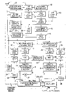
FIGURE 1 shows the radio receiver portions of a DTV receiver constructed in
accordance with the invention, which receiver is capable of receiving either
QAM or
VSB digital TV signals. An antenna 1 is a representative source of TV signals
in ultra
high frequency (UHF) band, or possibly in the very high frequency (VHF) band,
which TV signals are applied to a radio-frequency (RF) amplifier 2. The Rr
amplifier
2 is provided with a tracking preselection filter for selecting a portion of
the one of the
television broadcast bands the television signal selected for reception
reposes in. The
RF amplifier 2 is reverse-AGC'd in delayed response to AGC signals applied to
RF
amplifier 2 via an AGC delay circuit 3. The RF amplifier 2 supplies amplified
response to the television signal selected for reception.
This amplified response is mixed with a super-heterodyning signal from a first
local oscillator 10 for upconversion to a high intermediate-frequency-band,
which is
above the highest frequency television channel in the ultra-high frequency
(UHF)
1 ~ spectrum. In line with current TV practice, the first local oscillator 10
is usually a
frequency synthesizer for generating the super-heterodyning signal of a
frequency in
selected ratio with the frequency of a component controlled oscillator, with
the
frequency of the controlled oscillator being controlled by AFT signal. This
preferred
practice results in the sensitivity of the super-heterodyning signal frequency
to AFT
signal being substantially the same for all received TV channels. The 6-MHz-
wide
selected radio-frequency signal supplied by the RF amplifier 2 is upconverted
to a
high-band intermediate-frequency signal in a first mixer 11, which preferably
is of a
doubly-balanced linear-multiplication type. The high-band intermediate-
frequency
signal is centered at an ultra-high frequency above that portion of the UHF
band
? ~ containing assigned channels for television broadcasting, placing the
image
frequencies well above 1 GHz so they are easily rejected by a bandpass
coupling
network at the output of the first mixer 11.
A high-intermediate-frequency-band buffer amplifier 12 applies the
high-band IF signal to a surface-acoustic-wave (SAW) filter 13. The buffer
amplifier
12 provides fixed gain to make up the 10 - 12 dB insertion loss of the SAW
filter 13
9
CA 02262329 1999-02-19
and drives the SAW filter 13 from a fixed source impedance chosen to avoid
unwanted reflections. The SAW filter 13 has a substantially linear-phase,
flat-amplitude response that has -1 dB to -1 dB bandwidth of substantially 6
MHz,
which passband is symmetrical around a midband frequency. By way of example,
the
UHF IF signal can be centered at 916 MHz. A gallium arsenide SAW filter 13 can
be
operated satisfactorily in this frequency range. The response of the SAW
filter 13 is
supplied to a second mixer 14 for downconversion to a low-band
intermediate-frequency signal centered at a very high frequency below that
portion of
the VHF band containing assigned channels for television broadcasting. The low-
band IF signal can be centered at about 44 MHz, as common in analog TV
practice.
A local oscillator 20, which is preferably of a crystal-controlled type,
supplies a
heterodyning signal of stable fixed frequency to the second mixer 14 for
implementing the downconversion therein. The second mixer 14 is preferably of
a
doubly-balanced linear-multiplication type.
1 ~ A low-intermediate-frequency-band buffer amplifier 15 applies the low-band
IF signal to a surface-acoustic-wave (SAW) filter 16 designed for flat
response over at
least a 6 MHz bandwidth. The buffer amplifier 15 provides fixed gain to make
up the
10 - 12 dB insertion loss of the SAW filter 16 and drives the SAW filter 16
from a
fixed source impedance chosen to avoid unwanted reflections. The SAW filter 16
has
a substantially linear-phase response over a bandwidth in excess of 6 MHz, so
that the
earlier SAW filter 13 determines the channel characteristics of the first IF
amplifier
chain. A lithium niobate SAW filter 16 can be operated satisfactorily in the
frequency
range centered at about 44 MHz. The response of the SAW filter 16 is supplied
as
input signals to automatic-gain-controlled low-intermediate-frequency-band
(VHF)
2~ amplifiers 17 and 27. The low-IF-band amplifier 17 supplies its response as
input
signal to a third mixer 18 for supplying a final intermediate-frequency signal
for
digitization by an analog-to-digital converter 19 for application to digital
synchrodyne
circuitry 4, which synchronously detects in-phase (I) QAM carrier wave
modulation
and synchronously detects quadrature-phase (Q) QAM carrier wave modulation.
The
low-IF-band amplifier 27 supplies its response as input signal to a third
mixer 28 for
supplying a final intermediate-frequency signal for digitization by an analog-
to-digital
CA 02262329 1999-02-19
converter 29 for application to digital synchrodyne circuitry 5, which
synchronously
detects in-phase (I) VSB carrier wave modulation and synchronously detects
quadrature-phase (Q) VSB carrier wave modulation.
Insofar as the invention is concerned, in FIGURE 1 elements 2, 10 - 17, 20
and 27 constitute front-end circuitry for supplying penultimate intermediate-
frequency
signals to the third mixers 18 and 28. In the triple-conversion radio receiver
shown in
FIGURE 1 these penultimate intermediate-frequency signals are the second
intermediate frequency signals in the VHF band.
The response of the AGC'd IF amplifier 17 and VHF local oscillations from a
voltage-controlled third local oscillator 30 are applied as first and second
input
signals, respectively, to the third mixer 18. The third mixer 18 is for
downconverting
the amplified first VHF intermediate-frequency signal from the AGC'd IF
amplifier
17 to generate a first final intermediate-frequency signal offset a few MHz
from
baseband for digitization by the ADC 19.
1 ~ Digital synchrodyne circuitry 4 is designed for responding to QAM DTV
signal in this first final intermediate-frequency signal to recover respective
in-phase
(I) and quadrature-phase (Q) baseband signals that are descriptive of QAM
symbols.
A digital multiplier 31, which in order to secure speedy operation is
preferably
implemented in read-only memory (ROM), multiplies these I and Q baseband
signals
together. The resulting product which contains samples descriptive of a low
frequency beat term and of a term at symbol rate is converted to analog form
by a
digital-to-analog converter 32. The term at symbol rate in the DAC 32 response
is
supplied to an automatic-frequency-and-phase-control detector 33, and the AFPC
detector 33 response adjusts the frequency and phase of the voltage-controlled
third
2p local oscillator 30 to reduce the low frequency beat term in the DAC 32
response to
zero frequency. This feedback control of the voltage-controlled third local
oscillator
is a species of Costas loop. A QAM automatic-gain-control detector 34 responds
to the DAC 32 response to generate a first input signal for an AGC signal
combiner
2~, which applies an automatic-gain-control (AGC) signal to the low-IF-band
11
CA 02262329 1999-02-19
amplifier 17. In order better to preserve linearity of the QAM digital
modulation in
the low-IF-band amplifier 17 response, reverse AGC is employed with this
amplifier.
The response of the AGC'd IF amplifier 27 and VHF local oscillations from a
voltage-controlled third local oscillator 35 are applied as first and second
input
S signals, respectively, to the third mixer 28. The third mixer 28 is for
downconverting
the amplified second VHF intermediate-frequency signal from the AGC'd IF
amplifier 27 to generate a second final intermediate-frequency signal offset a
few
MHz from baseband for digitization by the ADC 29.
Digital synchrodyne circuitry 5 is designed for responding to VSB DTV signal
in this second final intermediate-frequency signal to recover respective in-
phase (I)
and quadrature-phase (Q) baseband signals, at the least the former of which
baseband
signals is descriptive of VSB AM symbols. The quadrature-phase baseband signal
from the synchrodyne circuitry 5 is converted to analog form by a digital-to-
analog
converter 36, and a lowpass filter 37 extracts a low frequency beat term from
the
1 ~ DAC 36 response for application to the voltage-controlled third local
oscillator 35 as
an automatic-frequency-and-phase-control (AFPC) signal therefor. The in-phase
baseband signal from the synchrodyne circuitry 5 is converted to analog form
by a
digital-to-analog converter 38, and a VSB automatic-gain-control detector 34
responds to the DAC 38 response to generate a second input signal for an AGC
signal
combiner 25, which applies an automatic-gain-control (AGC) signal to the
low-IF-band amplifier 27. In order better to preserve linearity of the VSB
digital
modulation in the low-IF-band amplifier 27 response, reverse AGC is employed
with
this amplifier.
Supposedly only one of the respective responses from the AGC detectors 34
2~ and 39 will indicate need for reducing radio receiver gain, so the AGC
signal
combiner 25 can be configured to act as an analog OR circuit for those
responses,
developing AGC signals responsive only to that one of the respective responses
from
the AGC detectors 34 and 39 which most indicates need for reducing radio
receiver
gain. The AGC signal combiner 25 supplies AGC signals to both the low-IF-band
amplifiers 17 and 27. The AGC signal combiner 25 forwards an AGC signal to the
12
CA 02262329 1999-02-19
AGC delay circuit 3 for reducing the gain of the RF amplifier 2 when very
strong
signal reception obtains.
The presence or absence in the DAC 36 response of a direct term arising from
the synchronous detection of ATSC signal pilot carrier is sensed by a
threshold
detector 21 operating as a VSB pilot carrier presence detector. Indications of
the
presence or absence of ATSC signal pilot carrier by the VSB pilot carrier
presence
detector 21 are used as control signal by a synchrodyne result selector 6.
These
indications are also supplied to an amplitude-and-group-delay equalizer 7 for
selecting the configuration of digital filters in the equalizer 7 to suit the
DTV signal
being currently received, depending on whether it is a QAM or a VSB AM signal.
Responsive to the VSB pilot carrier presence detector 21 indicating the
absence of ATSC signal pilot carrier, the synchrodyne result selector 6
selects the
in-phase baseband signal from the digital synchrodyne circuitry 4 for
application to an
amplitude-and-group-delay equalizer 7 as real sample stream and selects the
1 ~ quadrature-phase baseband signal from the digital synchrodyne circuitry 4
for
application to the equalizer 7 as imaginary sample stream. The two selection
procedures are performed synchronously, rather than in staggered phase.
Presuming
the sample rate to be 21.52 * 106 samples per second, the equalizer 7 can be
operated
as a fractional equalizer, with the digital filter circuitry in the equalizer
clocked at the
21.2 * 106 samples per second rate that is four times the baud rate of the QAM
symbols. Preferred designs use rate reduction filtering of the real and
imaginary
sample streams the equalizer 7 receives from the digital synchrodyne circuitry
4 for
Q AM. From the standpoint of utilizing hardware also used for equalization of
the
stream of real samples of demodulated VSB AM symbols, is convenient to
?~ time-division multiplex the real and imaginary sample streams of
demodulated QAM
symbols on an alternate sample basis and then to operate the rest of the
digital
equalization filtering on a dual-phase basis to provide complex equalization
during
QAM reception. Rate reduction filtering at the input of the equalizer 7 for
demodulated QAM can be such as to operate the equalizer as a synchronous
equalizer
for demodulated QAM or as a fractional equalizer for demodulated QAM. If the
equalizer 7 is operated as a fractional equalizer for demodulated QAM, it will
13
CA 02262329 1999-02-19
incorporate a rate reduction filter at its output to a trellis decoder 91
(shown in
FIGURE 8) for QAM signal.
In FIGURE 1, responsive to the VSB pilot carrier presence detector 21
indicating the presence of ATSC signal pilot carrier, the synchrodyne result
selector 6
selects the in-phase baseband signal from the digital synchrodyne circuitry 5
for
application to the amplitude-and-group-delay equalizer 7 as a real sample
stream and
selects a stream of arithmetic zeroes for application to the equalizer 7 as an
imaginary
sample stream. Presuming the sample rate in each stream to be 21.52 * 106
samples
per second, the equalizer 7 can be conditioned to operate as a fractional
equalizer
during VSB AM reception, with the digital filter circuitry in the equalizer
clocked at
the 21.52 * 106 samples per second rate, which is twice baud rate for the VSB
AM
symbols. Alternatively, the equalizer 7 can be provided with a rate reduction
filter at
its input. Still presuming the sample rate in each stream to be 21.52 * 106
samples per
second, the rate reduction filter can resample to the 10.76* 106 samples per
second
1 ~ baud rate for VSB AM, to operate the equalizer 7 as a synchronous
equalizer, or can
resample to a lower rate, such as 4/3 baud rate, to operate the equalizer 7 as
a
fractional equalizer with fewer taps. If the equalizer 7 is operated as a
fractional
equalizer for demodulated VSB AM, it will incorporate a rate reduction filter
at its
output to a trellis decoder 92 (shown in FIGURE 8) for VSB AM signal.
FIGURE 2 shows the radio receiver portions of a QAM/VSB DTV receiver
which differs from the FIGURE 1 QAM/VSB DTV receiver in that reverse-AGC'd
low-IF-band amplifiers 17 and 27 are replaced by a single reverse-AGC'd
low-IF-band amplifier 26 for amplifying the response of the SAW filter 16. The
third
mixers 18 and 28 receive the response of this single reverse-AGC'd low-IF-band
2~ amplifier 26 as their respective low-IF-band DTV input signals, rather than
the
respective responses of the reverse-AGC'd low-IF-band amplifiers 17 and 27.
The
response of the AGC signal combiner 25 is applied to the low-IF-band amplifier
26 as
reverse AGC signal. Insofar as the invention is concerned, in FIGURE 2
elements 2,
10 - 16, 20, and 26 constitute front-end circuitry for supplying penultimate
intermediate-frequency signals to the third mixers 18 and 28.
14
CA 02262329 1999-02-19
FIGURES 3 and 4 shows the radio receiver portions of QAM/VSB DTV
receivers that differ from those shown in FIGURES 1 and 2 respectively in that
rather
than the QAM/VSB CONTROL SIGNAL is not developed by the VSB pilot carrier
presence detector 21. Instead, the QAM/VSB CONTROL SIGNAL is developed by
an imaginary sample presence detector 22 connected to respond to the low-
frequency
quadrature-phase output signal from the VSB synchrodyning circuitry 5. The
imaginary sample presence detector 22 detects when there is substantial
variation in
the energy of the low-frequency quadrature-phase output signal, to furnish
indication
that a QAM signal is being received.
In still other embodiments of the invention, the QAM/VSB CONTROL
SIGNAL is developed in the following way, as the output signal from a
monostable
c~rcmt or its equivalent. A match filter supplies output pulses responsive to
the data
segment synchronization code groups, data field synchronization code groups,
or to
portions of data field synchronization code groups in the in-phase output
signal from
l~ the VSB synchrodyning circuitry ~, received as input signal by the match
filter.
These pulses are threshold detected to discriminate against noise, and the
threshold
detector pulses are supplied to a monostable circuit to place it into its
unstable state.
As Long as the monostable circuit is maintained in its unstable state, the
QAM/VSB
CONTROL SIGNAL indicates VSB AM reception. When the data synchronization
signal accompanying a VSB DTV signal is not detected, the monostable circuit
assumes its stable state, so the QAM/VSB CONTROL SIGNAL indicates
non-reception of VSB DTV signal from which QAM reception is inferred.
FIGURE ~ shows in more detail the digital circuitry 4 for synchrodyning
QAIVI DTV signals to baseband. The QAM synchrodyning circuitry 4 includes the
QAM in-phase synchronous detector 40 for generating the real portion of its
output
signal and the QAM quadrature-phase synchronous detector 45 for generating the
imaginary portion of its output signal. The QAM synchrodyning circuitry 4 is
essentially a complex digital multiplier which multiplies a real-to-complex
sample
converter 48 response to the digital samples from the ADC 19 by a complex
digital
samples of QAM carrier wave read from a read-only memory 49. The QAM
synchrodyning circuitry 4 includes a digital adder 46, a digital subtractor
47, and
CA 02262329 1999-02-19
respective first, second, third and fourth digital multipliers 41 - 44. The
QAM
in-phase synchronous detector 40 includes the multiplier 41, the multiplier
42, and the
adder 46 for adding the product output signals of the multipliers 41 and 42 to
generate
the real portion of the output signal of the QAM synchrodyning circuitry 4.
The first
digital multiplier 41 multiplies the real digital samples of final IF signal
supplied from
the real-to-complex-sample converter 48 by digital samples descriptive of the
cosine
of the QAM carrier that are read from a look-up table 491 in the ROM 49, and
the
second digital multiplier 42 multiplies the imaginary digital samples of final
IF signal
supplied from the real-to-complex-sample converter 48 by digital samples
descriptive
of the sine of the QAM carrier that are read from a look-up table 492 in the
ROM49.
The QANI quadrature-phase synchronous detector 45 includes the multiplier 43,
the
multiplier 44, and the subtractor 47 for subtracting the product output signal
of the
multiplier 43 from the product output signal of the multiplier 44 to generate
the
imaginary portion~of the output signal of the QA1~I synchrodyning circuitry 4.
The
1 ~ third digital multiplier 43 multiplies the real digital samples of final
IF signal supplied
from the real-to-complex-sample converter 48 by digital samples descriptive of
the
sine of the QAM carrier that are read from the look-up table 492 in the ROM
49, and
the fourth digital multiplier 44 multiplies the imaginary digital samples of
final IF
signal supplied from the real-to-complex-sample converter 48 by digital
samples
descriptive of the cosine of the QAVI carrier that are read from the look-up
table 491
in the ROM 49.
FIGURE 6 shows in more detail the digital circuitry 5 for synchrodyning VSB
DTV signals to baseband. The VSB synchrodyning circuitry 5 includes the VSB
in-phase synchronous detector 50 for generating the real portion of its output
signal
2~ and the VSB quadrature-phase synchronous detector 55 for generating the
imaginary
portion of its output signal. The VSB synchrodyning circuitry 5 is essentially
a
complex digital multiplier which multiplies a real-to-complex sample converter
58
response to the digital samples from the ADC 29 by a complex digital samples
of
QAM carrier wave read from a read-only memory 59. The VSB synchrodyning
circuitry 5 includes a digital adder 56, a digital subtractor 57, and
respective first,
second, third and fourth digital multipliers 51 - 54. The VSB in-phase
synchronous
16
CA 02262329 1999-02-19
detector 50 includes the multiplier 51, the multiplier 52, and the adder 56
for adding
the product output signals of the multipliers 51 and 52 to generate the real
portion of
the output signal of the VSB synchrodyning circuitry 5. The first digital
multiplier 51
multiplies the real digital samples of final IF signal supplied from the
real-to-complex-sample converter 58 by digital samples descriptive of the
cosine of
the VSB carrier that are read from a look-up table 591 in the ROM 59, and the
second
digital multiplier 52 multiplies the imaginary digital samples of final IF
signal
supplied from the real-to-complex-sample converter 58 by digital samples
descriptive
of the sine of the VSB carrier that are read from a look-up table 592 in the
ROM 59.
The VSB quadrature-phase synchronous detector 55 includes the multiplier 53,
the.
multiplier 54, and the subtractor 57 for subtracting the product output signal
of the
multiplier 53 from the product output signal of the multiplier 54 to generate
the
imaginary portion of the output signal of the VSB synchrodyning circuitry 5.
The
third digital multiplier 53 multiplies the real digital samples of final IF
signal supplied
1 ~ from the real-to-complex-sample converter 58 by digital samples
descriptive of the
sine of the VSB carrier that are read from the look-up table 592 in the ROM
59, and
the fourth digital multiplier 54 multiplies the imaginary digital samples of
final IF
signal supplied from the real-to-complex-sample converter 24 by digital
samples
descriptive of the cosine of the VSB carrier that are read from the look-up
table 591 in
the ROM 59.
FIGURE 7 shows in detail a representative construction of the sample clock
generator 8. This construction includes a voltage-controlled oscillator 80
that
generates cissoidal oscillations nominally of 21.5? MHz frequency. The
oscillator 80
is a controlled oscillator, the frequency and phase of its oscillations being
controlled
by an automatic frequency and phase control (AFPC) signal voltage. This AFPC
signal voltage is generated by an automatic frequency and phase control (AFPC)
detector 81, which compares frequency-divided response to the oscillations of
the
oscillator 80 with a 10.76 MHz reference carrier supplied via an analog 10.76
MHz
bandpass filter 82. Preferably, oscillator 80 is of a type using a crystal for
stabilizing
the natural frequency and phase of its oscillations. A symmetrical clipper or
limiter
83 generates an essentially squarewave response to these cissoidal
oscillations, which
17
CA 02262329 1999-02-19
is used as the first clock signal for timing the sampling of the final IF
signal in the
ADC 22. A frequency-divider flip-flop 84 responds to transitions of the first
clock
signal in a prescribed sense for generating another square wave with a
fundamental
frequency of 10.76 MHz, half the frequency of the oscillations of the
oscillator 80.
This frequency-divided response to the oscillations of the oscillator 80 is
supplied to
the AFPC detector 81 for comparison with the 10.76 MHz reference carrier
supplied
via the 10.76 MHz bandpass filter 82. The frequency-divider flip-flop 84 also
supplies squarewave output signal with a fundamental frequency of 10.76 MHz to
an
AND circuit 85 to be ANDed with the first clock signal for generating a second
clock
signal used by rate reduction filtering in the equalizer 7.
The 21.52 MHz reference carrier supplied from the VCO 80 is generated by
extracting a component of the received DTV signal as synchrodyned to baseband,
which component is of a frequency that is a subharmonic of the symbol
frequency (or
baud frequency), and multiplying that subharmonic of the symbol frequency by
an
1 ~ appropriate factor in frequency multiplier circuitry. The details of this
procedure will
now be specifically described, first presuming the received DTV signal is a
VSB
signal with a 10.76 MHz symbol frequency or baud rate, and then presuming the
received DTV signal is a QAM signal with a 5.38 MHz symbol frequency or baud
rate.
A digital multiplexer 86 responds to the pilot carrier presence detector 21
detecting pilot carrier accompanying the received DTV signal, which is
indicative that
the received DTV signal is a VSB signal, to select the real samples of this
signal
supplied from the VSB in-phase synchronous detector 50 for application to a
bandpass FIR digital filter 87 that provides a selective response centered at
5.38 MHz,
2~ which selects the first subharmonic of symbol frequency from the VSB
signal.
Further frequency multiplication of the x.38 MHz is performed in the analog
regime
to avoid undersampling problems that arise when attempting to perform further
frequency multiplication in the digital regime. An digital-to-analog converter
(DAC)
88 converts the filter 87 response to analog form for application to full-wave
rectification circuitry 89, which generates harmonics of the filter 87
response
including a strong 10.76 MHz component as second harmonic of 5.38 MHz. The
18
CA 02262329 1999-02-19
analog bandpass filter 82 responds to this 10.76 MHz second harmonic to supply
the
AFPC detector 81 with 10.76 MHz reference carrier input signal.
The digital multiplexer 86 responds to the pilot carrier presence detector 21
not detecting pilot carrier accompanying the received DTV signal, which is
indicative
that the received DTV signal is a QAM signal, to select the output signal of a
squaring
circuit 8A for application to the bandpass filter 87 that provides a selective
response
centered at 5.38 MHz. A bandpass FIR digital filter 8B that provides a
selective
response centered at 2.69 MHz for selecting the 2.69 MHz first subharmonic of
the
symbol frequency of a baseband QAM signal supplies input signal to the
squaring_~ '
circuit 8A, which generates harmonics of the filter SB response including a
strong
x.38 MHz component. This baseband QAM signal can be supplied either from the
QANL in-phase synchronous detector 40, as shown in FIGURE 7, or from the QAM
quadrature-phase synchronous detector 45. The squaring circuit 8A is shown in
FIGURE 7 as a digital multiplier receiving the filter 8B response both as
multiplier
1 p and multiplicand. The squaring circuit 8A can be constructed from logic
gates as a
digital multiplier, but for the sake of speedier operation is better provided
by a ROM
storing a look-up table of squares. An absolute-value circuit can be used as a
substitute for the squaring circuit in generating harmonics of the response of
a
preceding filter, but produces weaker second harmonics and so is not
preferred.
FIGURE 7 also shows a representative construction of a first address
generator 60 that supplies addresses to a cosine look-up table portion 491 and
a sine
look-up table portion 492 of the ROM 49 that provides complex-number digital
descriptions of two phasings of the QAM carrier, as translated to a final
intermediate
frequency and in quadrature relationship with each other. Transitions of the
first
2~ clock signal are counted by a first address counter 61 in the first address
generator 60
to generate a basic first address signal. This basic first address signal is
applied as a
first summand to a digital adder 62. A first address correction signal, which
is applied
to the adder 62 as a second summand, adds to the basic first address signal in
the
adder 62 for generating as a sum output signal a corrected first address
signal for
addressing both the cosine look-up table portion 491 and the sine look-up
table
portion 492 of the ROM 49. A symbol-clock-rotation detector 63 responds to the
19
CA 02262329 2001-06-19
sequence of real samples of QAM signal as synchrodyned to baseband by the QAM
in-
phase synchronous detector 40 and to the sequence of imaginary samples of QAM
signal as synchrodyned to baseband by the QAM quadrature-phase synchronous
detector 45. The symbol-clock-rotation detector 63 detects the misphasing
between
symbol clocking done at the receiver in accordance with the first clock signal
and
symbol clocking done at the transmitter, as evidenced in the received QAM
signal
heterodyned to a final intermediate frequency that is a submultiple of its
symbol
frequency. Several types of symbol-clock-rotation detector 63 are described
and
background literature describing certain of them are catalogued in U. S.
patent No.
5,115,454 issued 19 May 1992 to A. D. Kucar, entitled METHOD AND
APPARATUS FOR CARRIER SYNCHRONIZATION AND DATA
DETECTION. A digital lowpass filter 64 averages over many samples (e. g.,
several
million) the misphasing of the symbol clocking done at the receiver as
detected by the
symbol-clock-rotation detector 63 to generate the first address correction
signal
supplied to the adder 62 to correct the basic first address. Averaging over so
many
samples can be done by procedures which accumulate lesser numbers of samples
and
dump them forward at a reduced sample rate for further accumulation,
accumulation
and subsampling being repeated a few times with progressively lower
subsampling
rates.
FIGURE 7 also shows a representative construction of a second address
generator 70 that supplies addresses to a cosine look-up table portion 591 and
a sine
look-up table portion 592 of the ROM 59 that provides complex-number digital
descriptions of two phasings of the VSB carrier, as translated to a final
intermediate
frequency and in quadrature relationship with each other. Transitions of the
first clock
signal axe counted by a second address counter 71 in the second address
generator 70 to
generate a basic second address signal. This basic second address signal is
applied as a
first summand to a digital adder 72. A second address correction signal, which
is
applied to the adder 72 as a second summand, adds to the basic second address
signal
in the adder 72 for generating as a sum output signal a corrected second
address signal
for addressing both the cosine look-up table portion 591 and the sine look-up
table
portion 592 of the ROM 59.
CA 02262329 1999-02-19
FIGURE 7 shows a clocked digital delay line 73 for delaying the samples
from the in-phase synchronous detector 50 by a prescribed number of sample
periods
prior to their being applied as input signal to a quantizer 74, which supplies
the
quantization level most closely approximated by the sample currently received
by the
quantizer 74 as input signal. The quantization levels can be inferred from the
energy
of the pilot carrier accompanying the VSB signal or can be inferred from the
result of
envelope detection of the VSB signal. The closest quantization level selected
by the
quantizer 74 as its output signal has the corresponding quantizer 74 input
signal
subtracted therefrom by a digital adder/subtractor 75, which is operated as a
clocked
element by including a clocked latch at its output. The difference output
signal frcsm
the adder/ subtractor 75 describes the departure of the symbol levels actually
recovered from those that should be recovered, but whether the polarity of the
departure is attributable to symbol misphasing being leading or lagging
remains to be
resolved.
1 ~ The samples from the in-phase synchronous detector 50 applied as input
signal
to the clocked digital delay line 73 are applied without delay as input signal
to a
mean-square-error gradient detection filter 76. The filter 76 is a
finite-impulse-response (FIR) digital filter having a (-1/2), 1, 0, (-1),
(+I/2) kernel, the
operation of which is clocked by the first sampling clock. The prescribed
number of
sample periods of delay provided by the clocked digital delay line 73 is such
that filter
76 response is in temporal alignment with the difference signal from the
adder/subtractor 75. A digital multiplier 77 multiplies the difference signal
from the
adder/subtractor 7~ with the filter 76 response to resolve this issue. The
sign bit and
the next most significant bit of the two's complement filter 76 response
suffice for the
2~ multiplication, which permits simplification of the digital multiplier 77
structure. The
samples of the product signal from the digital multiplier 77 are indications
of the
misphasing of the symbol clocking done at the receiver that are averaged over
many
samples (e. g., several million) by a digital lowpass filter 78 for generating
the second
address correction signal supplied to the adder 72 to correct the basic second
address.
The symbol synchronization techniques used in the second address generator
70 shown FIGURE 6 are of the same general type as S. U. H. Qureshi describes
for
21
CA 02262329 1999-02-19
use with pulse amplitude modulation (PAM) signals in his paper "Timing
Recovery
for Equalized Partial-Response Systems, IEEE Transactions on Communications,
Dec. 1976, pp. 1326 - 1330. These symbol synchronization techniques as used in
connection with symbol synchronization for VSB signals are specifically
described by
C. B. Patel and the inventor in their earlier-filed applications referenced
earlier in this
specification. In preferred designs of the general type of second address
generator 70
shown in FIGURE 7, the clocked digital delay line 73 does not exist as a
separate
element; instead, an input signal to the quantizer 74 with the requisite
number of
sample periods of delay for the difference signal from the adder/subtractor 75
being
temporally aligned with the filter 76 response is taken from the tapped
digital delay
line included in the filter 76 for supplying differentially delayed samples to
be
weighted by the (-1/2), 1, 0, (-1), (+1/2) kernel before being summed to
generate the
filter 76 response.
FIGURE 8 shows the amplitude-and-group-delay equalizer 7, which converts
1 ~ a baseband response with an amplitude-versus-frequency characteristic that
tends to
cause inter-symbol error to a more optimum amplitude-versus-frequency
characteristic that minimizes the likelihood of inter-symbol error. The
amplitude-and-group-delay equalizer 7, which is also shown in the FIGURES 1-4,
can
be a suitable one of the monolithic ICs available off the-shelf for use in
equalizers.
Such an IC includes a multiple-tap digital filter used for amplitude-and-group-
delay
equalization, the tap weights of which filter are programmable; circuitry for
selectively accumulating training signal and temporarily storing the
accumulation
results; and a microcomputer for comparing the temporarily stored accumulation
results with an ideal training signal as known a priori and for calculating
updated tap
2~ weights of the multiple-tap digital filter used for amplitude-and-group-
delay
equalization.
During VSB AIVI reception, the real response of the amplitude-and-group-
delay equalizer 7 is applied as input signal to one-dimensional symbol
decoding
circuitry 91, which performs the symbol decoding that recovers symbol-decoded
digital data streams from a VSB-origin signal. A VSB signal in accordance with
the
ATSC standard uses trellis coding of the data in all data segments except the
initial
22
CA 02262329 2001-06-19
data segment of each data field, which contains field synchronization code
groups that
are not subject to trellis coding. As in the prior art, one of the symbol-
decoded digital
data streams that the symbol decoding circuitry 91 supplies, which is to be
employed
for further data processing is generated by trellis-decoding the results of
data-slicing
procedures, and optimal Viterbi decoding techniques are customarily employed.
As in
the prior art, another of the symbol-decoded digital data streams that the
symbol
decoding circuitry 91 supplies, which is to be employed for controlling data
handling
by the receiver responsive to synchronization information contained in the
received
QAM-origin signal, is generated using data-slicing procedures without
subsequent
trellis decoding. The symbol decoding circuitry 91 preferably departs from
usual prior-
art practice by utilizing data-slicing techniques similar to those described
by the
inventor in U. S. patent No. 5,748,226 issued 5 May 1998, entitled DIGITAL
TELEVISION RECEIVER WITH ADAPTIVE FILTER CIRCUITRY FOR
SUPPRESSING NTSC CO-CHANNEL INTERFERENCE.
During QAM reception both the real and the imaginary responses of the
amplitude-and-group-delay equalizer 7 are applied as input signal to two-
dimensional
symbol decoding circuitry 92, which performs the symbol decoding that recovers
symbol-decoded digital data streams from a QAM-origin signal. Presuming that
the
QAM-origin signal contains data synchronizing information corresponding with
that in
the VSB-origin signal, one of these symbol-decoded digital data streams is a
trellis-
decoded digital data stream supplied for further data processing, and another
of these
symbol-decoded digital data streams is generated by data-slicing without
subsequent
trellis decoding. This latter symbol-decoded digital data stream is employed
for
controlling data handling by the receiver responsive to synchronization
information
contained in the received VSB-origin signal.
A digital-signal multiplexes 93 functions as a data source selector that
selects as
its response either a first or a second one of two digital input signals
thereto, the
selection being controlled by the VSB pilot presence detector 21 for detecting
the zero-
frequency term of the real samples from the VSB synchrodyne circuitry 5. When
the
zero-frequency term has essentially zero energy, indicating the absence of
23
.,..,., , ......,.....,...... <..:,"",.",.,",.,..,~.,"....,._,..._
............."." .-,_,.,..".-.""....,.,."."M"...."...,....,,."~.,.,......
"..~,..
CA 02262329 1999-02-19
pilot carrier signal that accompanies a VSB signal, the multiplexes 93
selectively
responds to its first digital input signal, selecting as the source of its
digital data
output the two-dimensional symbol decoding circuitry 91 that decodes the
symbols
received in the QAM signal. When the zero-frequency term has substantial
energy,
indicating the presence of pilot carrier signal that accompanies a VSB signal,
the
multiplexes 93 selectively responds to its second digital input signal,
selecting as the
source of its digital data output the one-dimensional symbol decoding
circuitry 92 that
decodes the symbols received in the VSB signal.
The data selected by the data source selection multiplexes 93 are applied to~a
data de-interleaves 94 as its input signal, and the de-interleaved data
supplied from the
data de-interleaves 94 are applied to a Reed-Solomon decoder 95. The data
de-interleaves 94 is often constructed within its own monolithic IC and is
made so as
to respond to the output indications from the VSB pilot carrier presence
detector 21 to
select the de-interleaving algorithm suitable to the DTV signal currently
being
1 ~ received, whether it be of QAM or VSB type; this is a mere matter of
design. The
Reed-Solomon decoder 95 is often constructed within its own monolithic IC and
is
made so as to respond to the output indications from the VSB pilot carrier
presence
detector 21 to select the appropriate Reed-Solomon decoding algorithm for the
DTV
signal currently being received, whether it be of QAM or VSB type; this also
is a
mere matter of design. Error-corrected data are, supplied from the Reed-
Solomon
decoder 95 to a data de-randomizer 96, which responds to these data for
regenerating
a signal randomized prior to transmission to the DTV receiver, which
regenerated
signal comprises packets of data for a packet sorter 97. The data de-
randomizer 96 is
made so as to respond to the output indications from the VSB pilot carrier
presence
2~ detector 21 to select the appropriate data de-randomizing algorithm for the
DTV
signal currently being received, whether it be of QAM or VSB type; the
selection of
these algorithms is a mere matter of design, too.
First data synchronization recovery circuitry 98 recovers the data
synchronizing information included in the data output of the two-dimensional
symbol
decoding circuitry decoder 91, and second data synchronization recovery
circuitry 99
recovers the data synchronizing information included in the data output of the
24
CA 02262329 1999-02-19
one-dimensional symbol decoding circuitry 92. A data sync selector 100 selects
between the data synchronizing information as provided by the data sync
recovery
circuitry 98 and as provided by the data sync recovery circuitry 99, the
selection being
controlled by the VSB pilot earner presence detector 21 for detecting the
S zero-frequency term of the real samples from the VSB synchrodyne circuitry
5.
When the zero-frequency term has essentially zero energy, indicating the
absence of
pilot earner signal that accompanies a VSB signal, the data sync selector 100
selects
for its output signals the data synchronizing information provided by the data
sync
recovery circuitry 98. When the zero-frequency term has substantial energy,
indicating the presence of pilot carrier signal that accompanies a VSB signal,
the data
sync selector 100 selects for its output signals the data synchronizing
information
provided by the data sync recovery circuitry 99.
When the data sync selector 100 selects for its output signals the data
synchronizing information provided by the data sync recovery circuitry 99, the
initial
1 ~ data lines of each data field are selected for application to the
amplitude-and-group-delay equalizer 7 as training signal. The occurrences of
two
consecutive 63-sample PR sequences are detected within the data sync recovery
circuitry 99 to provide data-field indexing information to the data sync
selector 100.
The standards for a QAM DTV signal are not as well defined at this time as
the standards for a VSB DTV signal. A 32-state QAM signal provides sufficient
capacity for a single HDTV signal, without having to resort to compression
techniques outside MPEG standards, but commonly some compression techniques
outside MPEG standards are employed to encode the single HDTV signal as a
16-state QAM signal. The occurence of a prescribed 24-bit word is detected by
the
2~ data sync recovery circuitry 99 to generate data-field indexing information
for
application to the data sync selector 100. A multiplexes within the data sync
selector
100 selects between the data-field indexing information respectively supplied
by the
data sync recovery circuitry 98 and the data sync recovery circuitry 99; the
data-field
indexing information thus selected is supplied to the data de-interleaves 94,
the
Reed-Solomon decoder 95, and the data de-randomizer 96. At the time this
specification is written there is no training signal included in the QAM DTV
signal.
CA 02262329 1999-02-19
Accordingly, the amplitude-and-group-delay equalizer 7 is arranged to provide
a flat
amplitude-versus-frequency characteristic in response to the VSB pilot carrier
presence detector 21 indicating the absence of pilot carrier, and the VSB
training
signal selected by the data sync recovery circuitry 99 is wired through the
data sync
selector 100 without need for a multiplexes. Also, there is no data line
synchronization signal for QAM DTV transmission, at least not one selected as
a
standard. The data sync recovery circuitry 98 includes counting circuitry for
counting
the samples in each data field to generate intra-data-field synchronizing
information.
This intra-data-field synchronizing information and the intra-data-field
synchronizing
information (such as data line count) generated by the data sync recovery
circuitry~99
are selected between by appropriate multiplexers in the data sync selector
100, for
application to the data de-interleaves 94, the Reed-Solomon decoder 95, and
the data
de-randomizer 96, as required.
Data synchronization can alternatively be accomplished before symbol
1 ~ decoding, using match filters that generate spike responses to
synchronization code
sequences in the selector 6 response or in the equalizer 7 response. The
filters that
generate spike responses to synchronization code sequences are preferably
supplied
input signals with sampling rate reduced to the baud rate or symbol rate of
ATSC
signal, rather than their input signals being the over-sampled responses of
synchrodyne circuits 4 and 5, in order to reduce the number of samples in the
respective kernel of each match filter. The filters that generate spike
responses to
synchronization code sequences are preferably connected to receive the
equalizer 7
response to reduce the effect that mufti-path reception has on data
synchronization.
The packet sorter 97 sorts packets of data for different applications,
responsive
2~ to header codes in the successive packets of data. Packets of data
descriptive of the
audio portions of the DTV program are applied by the packet sorter 97 to a
digital
sound decoder 101. The digital sound decoder 101 supplies left-channel and
right-channel stereophonic sound signals to a plural-channel audio amplifier
102 that
drives the plurality of loudspeakers 103, 104. Packets of data descriptive of
the video
portions of the DTV program are applied by the packet sorter 97 to an MPEG
decoder
105, such as of MPEG-2 type. The MPEG decoder 105 supplies horizontal (H) and
26
CA 02262329 2001-06-19
vertical (V) synchronizing signals to kinescope deflection circuitry 106 that
provides
for the raster scanning of the viewing screen of a kinescope 107. The MPEG
decoder
105 also supplies signals to the kinescope driver amplifiers 108 for applying
amplified
red (R), green (G) and blue (B) drive signals to the kinescope 107. In
variations of the
DTV receiver shown in any one of the FIGURES 1, 2, 3 and 4 and in FIGURE 8, a
different display device may be used instead of or in addition to the
kinescope 107, and
the sound recovery system may be different, consisting of but a single audio
channel,
or being more elaborate than a simple stereophonic reproduction system.
The real-to-complex-sample converters 48 and 58 can employ Hilbert
transform generation filters and delay compensation circuitry as described by
C. B.
Patel and the inventor in their U. S. patent No. 5,479,449 issued 26 December
1995,
entitled DIGITAL VSB DETECTOR WITH BANDPASS PHASE TRACKER, AS
FOR INCLUSION IN AN HDTV RECEIVER, and incorporated herein by
reference. Alternatively, the real-to-complex-sample converters 48 and 58 can
employ
Rader filters as described by C. B. Patel and the inventor in their U. S.
patent No.
5,548,617 issued 20 October 1996, entitled DIGITAL VSB DETECTOR WITH
BANDPASS PHASE TRACKER USING RADER FILTERS, AS FOR USE IN
AN HDTV RECEIVER, and incorporated herein by reference. Or, the
real-to-complex-sample converters 48 and 58 can employ Ng filters as described
by C.
B. Patel and the inventor in U. S. patent No. 5,731,848 issued 24 March 1998,
entitled
DIGITAL VSB DETECTOR WITH BANDPASS PHASE TRACKER USING NG
FILTERS, AS FOR USE IN AN HDTV RECEIVER.
Preferably the lowest frequency of the final IF signal is above 1 MHz, to keep
the ratio of the highest frequency of the final IF signal thereto
substantially below 8:1
and thereby ease the filtering requirements for the real-to-complex-sample
converters 48
and 58. To satisfy this preference in regard to the QAM signal alone, the
lowest carrier
frequency for the QAM carrier in the final IF signal is 3.69 MHz. To satisfy
this
preference in regard to the VSB signal alone, the lowest the carrier frequency
for the
VSB carrier in the final If ~signaI could be is 1.31 MHz, presuming its full
27
CA 02262329 2001-06-19
sideband to be above its vestigial sideband in frequency, or 6.38 MHz,
presuming its
full sideband to be below its vestigial sideband in frequency.
As taught by C. B. Patel and the inventor in their U. S. patent No. 5,606,579
issued 25 February 1997, entitled DIGITAL VSB DETECTOR WITH FINAL I-F
CARRIER AT SUBMULTIPLE OF SYMBOL RATE, AS FOR USE IN AN
HDTV RECEIVER, there is a strong preference that the carrier of the signal
being
synchrodyned to baseband in the digital regime be at a submultiple of a
multiple of the
symbol rate. This makes practical the storage of digital carrier signals in
read-only
memory, rather than having to digitize analog carrier signals on a continuing
basis.
If the sample rate in the ADC 19 is established by the first clock signal from
the
sample clock generator 8 to be the minimal 21.52 * 106 samples per second
required for
proper demodulation of a QAM signal with 5.38 * 1 O6 symbols per second,
preferably
the final intermediate frequency to which the carrier of a QAM DTV signal is
translated
is not higher than 5.38 MHz, so that it can be sampled at least four times per
cycle. If
the QAM carrier of the final IF signal must lie between 3.69 MHz and 5.38 MHz,
inclusive, the QAM carrier could be at the 7'", 8'", 9'" or 10'" subharmonic
of 43.05
MHz, for example. The 7'" subharmonic of 43.05 MHz and 3'd subharmonic of
21.52
MHz, 5.38 MHz, is a clear favorite for the final intermediate frequency to
which the
QAM carrier should be translated. It permits symmetries in the addressing of
ROM 49
to be exploited to reduce the number of actual storage locations required.
From the
standpoint of keeping down the number of actual storage locations required in
the ROM
49, the I 1'" subharmonic of 43.05 MHz and 5'" subharmonic of 21.52 MHz, 3.587
MHz,
might be a suitable final intermediate frequency to which the QAM carrier is
translated,
but the real-to-complex-sample converter 48 must then be designed to provide
real-to-
complex-sample conversion down to 900 kHz.
If the sample rate in the ADC 29 is established by the first clock signal from
the
sample clock generator 8 to be the minimal 21.52 * 106 samples per second
required for
proper demodulation of a VSB signal with 10.76 * 106 symbols per
3O
28
CA 02262329 1999-02-19
second, the final intermediate frequency to which the carrier of a VSB DTV
signal is
translated cannot be higher than 5.38 MHz, or the symbol synchronization
techniques
adapted from Qureshi's techniques cannot be successfully employed. If the full
sideband of the VSB signal is to be below its vestigial sideband in frequency,
the
sample rate in the ADC 29 must be higher than 21.52 * 106 samples per second
(e. g.,
43.05 * 106 samples per second) in order that the carrier can be at least 6.38
MHz. To
avoid the higher sample rate in the ADC 29, the full sideband of the VSB
signal must
be above its vestigial sideband in frequency. This means that the
real-to-complex-sample converters 48 and 58 cannot practically employ Ng
filters
when the sample rate in the ADC 29 is 21.52 * 106 samples per second.
The carrier of the VSB signal as translated to final intermediate frequency
for
synchrodyning to baseband must lie in the range between 1.31 MHz and 3.62 MHz,
inclusive, if the final IF signal is to be constrained to a 1 - 9 MHz
frequency range.
The VSB carrier could be at the 5'n, 6'n, 7'n, 8'n, 9'n, 10'n, 11'n, 12'n,
13'n, 14'n or 15'n
1 ~ subharmonic of 43.05 MHz, for example. The 15'n subharmonic, 2.690 MHz,
appears
to be a good choice for the final intermediate frequency to which the VSB
carrier
should be translated, viewed from the standpoint of reducing the size of
carrier
look-up tables in ROM by utilizing symmetries in addressing. However, 2.690
MHz
is not the best choice if the QAM carrier in the final IF signal supplied to
the
synchrodyne circuitry 4 is 5.381 MHz, since the nominal frequencies of the
third local
oscillators 30 and 35 are then the same. Oscillators nearby each other that
are of
nearly the same frequencies have a tendency to oscillate in unison, which can
adversely affect the ability to control separately their respective
frequencies.
The 315' subharmonic of 43.05 MHz, 1.345 MHz, which is the 15'n
?5 subharmonic of 21.52 MHz, appears to be another good choice for the final
intermediate frequency to which the VSB carrier should be translated, from the
standpoint of reducing the size of carrier look-up tables in ROM by utilizing
symmetries in addressing. The 23"~ subharmonic of 43.05 MHz, 1.793 MHz, which
is
the 1 1 'n subharmonic of 21.52 MHz, may be chosen instead, however, to ease
the
design requirements on the real-to-complex-sample converter 58 insofar as how
low a
frequency real-to-complex-sample conversion must be provided.
29
CA 02262329 1999-02-19
FIGURE 9 is a table of design frequencies for the local oscillator used to
supply the oscillations used to heterodyne a penultimate intermediate-
frequency band
centered at 44 MHz down to various final intermediate-frequency bands for QAM
signals. The oscillations of the third local oscillator 30 are preferably
below the
penultimate IF band in order to lessen the possibility of the second harmonic
of the
oscillations interfering with any nearby frequency-modulation radio broadcast
receiver.
FIGURE 10 is a table of design frequencies for the local oscillator used to
supply the oscillations used to heterodyne a penultimate intermediate-
frequency band
centered at 44 MHz down to various final intermediate-frequency bands for VSB
y
signals, presuming the vestigial sideband to be located above the full
sideband in
frequency in both in the penultimate IF band and in the final IF band. This
type of
operation is associated with the ADCs 19 and 29 sampling at 43.05 * 106
samples per
second, rather than at 21.52 * 10~ samples per second, in which case a 4:1
rate
reduction filter would be used if the equalizer 7 were to be a synchronous
equalizer.
The first local oscillator 10 provides oscillations above the first
intermediate-frequency band to the mixer 11, so the vestigial sideband located
below
the full sideband in frequency in the received DTV channel is converted so as
to be
located above the full sideband in frequency in the first intermediate-
frequency band.
In order for the vestigial sideband to be located below the full sideband in
frequency
in the second or penultimate IF band, the second local oscillator 20 must
supply the
second mixer 14 oscillations at a frequency above the first intermediate-
frequency
band. In order for the vestigial sideband to be located above the full
sideband in
frequency in the second or penultimate IF band, the second local oscillator 20
must
2~ supply the second mixer 14 oscillations at a frequency below the first
intermediate-frequency band. If the first IF band is centered at 940 MHz, for
example, the second local oscillator 20 supplies oscillations at 896 MHz to
center the
penultimate IF band at 44 MHz. 896 MHz is above current UHF channel 83, so a
nearby NTSC receiver will not tune these second oscillations if they radiate
beyond
the DTV receiver. If the vestigial sideband is located above the full sideband
in
frequency in the second or penultimate IF band, the third local oscillator 35
must
CA 02262329 1999-02-19
supply the third mixer 28 with oscillations at a frequency below those in that
penultimate IF band, in order that the vestigial sideband be located above the
full
sideband in frequency in the final IF band.
FIGURE 11 is a table of design frequencies for the local oscillator used to
supply the oscillations used to heterodyne a penultimate intermediate-
frequency band
centered at 44 MHz down to various final intermediate-frequency bands for VSB
signals, presuming the vestigial sideband to be located below the full
sideband in
frequency both in the penultimate IF band and in the final IF band. The first
local
oscillator 10 provides oscillations above the first intermediate-frequency
band to the
mixer 1 l, so the vestigial sideband located below the full sideband in
frequency in the
received DTV channel is converted so as to be located above the full sideband
in
frequency in the first intermediate-frequency band. In order for the vestigial
sideband
to be located below the full sideband in frequency in the second or
penultimate IF
band, the second local oscillator 20 must supply the second mixer 14
oscillations at a
1 ~ frequency above the first intermediate-frequency band. If the first IF
band is centered
at 916 MHz, for example, the second local oscillator 20 supplies oscillations
at 960
MHz to center the penultimate IF band at 44 MHz. It is desirable that the
second
local oscillator 20 supplies oscillations at no higher a frequency than 960
MHz, in
order to minimize the possibility of interference with the aeronautical
navigation
band. If the vestigial sideband is located below the full sideband in
frequency in the
second or penultimate IF band, the third local oscillator 35 must supply the
third
mixer 28 with oscillations at a frequency below those in that penultimate IF
band, in
order that the vestigial sideband be located below the full sideband in
frequency in the
final IF band.
2~ Locating the second or penultimate IF band lower in frequency facilitates
the
third local oscillator 3~ oscillating at a frequency above this IF band. Such
arrangement permits the vestigial sideband to be located above the full
sideband in
frequency in the penultimate IF band and the vestigial sideband to be located
below
the full sideband in frequency in the final IF band. Such arrangement
alternatively
permits the vestigial sideband to be located below the full sideband in
frequency in
the penultimate IF band and the vestigial sideband to be located above the
full
31
CA 02262329 1999-02-19
sideband in frequency in the final IF band. The oscillating frequency of the
second
local oscillator 20 need not be as much removed from the first intermediate-
frequency
band, which eases design requirements in the UHF portions of the radio
receiver
portions of the DTV signal receiver. The penultimate IF band being at a lower
frequency makes satisfactory design of the SAW filter 16 more difficult,
however.
In the foregoing specification the ordinal numbers used as adjectives before
the terms "mixer" and "local oscillator" are in accordance with normal
engineering
parlance descriptive of their placement in the radio receiver. This parlance
is not
carried over into the claims which follow, except as these ordinal numbers may
appear in quotation marks. Ordinal numbers not in quotation.marks in the
claims y
merely refer to the consecutive order in which the elements referred to by
such ordinal
numbers first appear in a set of claims.
32