Note: Descriptions are shown in the official language in which they were submitted.
CA 02262553 2003-08-25
SPECIFICATION
METHOD AND DEVICE FOR VARIABLE
SPEED TRANSMISSION
TECHNICAL FIELD
The present invention relates to an apparatus for
spectrum spread communication using a CDMA mobile
communication system, and particularly for a CDMA variable
rate transmission method with stable performance for high-speed
transmission and a variable rate transmission apparatus based
on the method.
BACKGROUND ART
Active research and development have been carried out
for third-generation mobile communication systems. In the
next-generation third system, because multimedia
communications are considered as main service, there has been a
demand for the function of high capacity and for the function of
data transmission of various rates with the required minimum
transmission power on a flexible and high-quality basis. There
is much attention on a multiple access system using a spectrum
spread communication, i.e., a CDMA (Code Division Multiple
Access) system as the radio access for this next generation radio.
Spectrum spread communications based on direct
1
CA 02262553 1999-O1-29
sequence are communications in which an information signal is
multiplied by spreading which results in a transmission band
width wider than the information signal band width. The
spectrum spread communication has features such as low
probability of intercept, anti-interference, anti-multipath fading,
multiple access possibility, etc. The multiple accessing system
means that a plurality of mobile stations communicate
simultaneously with a base station. The performance of the
spectrum spread communication depends on a spreading factor.
The spreading factor indicates the ratio of the transmission band
to the information signal band, i.e., the ratio between a
spreading-code rate and an information transmission rate. One
obtained by representing the spreading factor in decibel (dB) is
called "processing gain". When the information transmission
rate is 10 kbps and the spreading-code rate is lMcps (chips per
second), for example, the spreading factor reaches 100 and the
processing gain results in 20dB.
As described above, the multiple access system using the
spectrum spread communication is called "CDMA". In the
present CDMA system, different spreading codes are used in
every user or channel to identify the users or channels.
It has been reported by Gillhauzen et. al from the
following reference that the CDMA system is superior to other
multiple access systems such as a TDMA (Time Division Multiple
Access) system in channel capacity (the number of channels in
Z
CA 02262553 1999-O1-29
the same band). The reference is as follows: "On the Capacity of
a Cellular CDMA System", IEEE Transactions on Vehicular
Technology vol. 40, No. 2, May.
In addition to this, the CDMA system has an advantage
that since all the radio cells (radio zones) are allowed to use the
same frequency, the CDMA system can relatively easily
implement diversity handoff (or soft handoffj which are not
handled well by the TDMA system. Further, in contrast with the
TDMA system, multipath signals, which might degrade quality
multi-path signals, are separated from others and identified by
RAKE reception and can be effectively synthesized in reverse.
Thus excellent transmission quality can be achieved with less
transmitting power.
Fig. 1 is a block diagram showing an up-link
transmission system employed in the conventional coherent
multicode DS-CDMA (Direct Sequence CDMA). In the up-link
transmission system, the length of one frame is lOms and user
data and control data are multiplexed on a time basis. In order
to detect an error produced in the frame, a 16-bit CRC (Cyclic
Redundancy Check) is used to perform error detection coding and
a 6-bit tail bit (Tail) is added thereto. Thereafter, convolutional
coding of a 1/3 rate which is included into some of a spreading
process is performed. Since the error detecting process is
completed for each frame, a structure applicable to packet
transmission is adopted in the conventional example.
CA 02262553 1999-O1-29
Fig. 2 is an explanatory view showing the insertion of
pilot symbols, used for estimation of fading, into coded data
(Coded Data) after having been interleaved in the conventional
up-link transmission system shown in Fig. 1. In the drawing, (a)
indicates the case in which a transmission rate (data rate) of
transmit data is less than 32 kbps and (b) indicates the case in
which the data rate is less than 128 kbps. As shown in Fig. 2,
the transmit data or its sequence is divided into slots every 0.5ms
after the completion of bit interleaving. In the case of a 32(128)
kbps code channel, 4(16)-bit pilots are inserted into the transmit
data sequence, after which data modulation (QPSI~ is performed
(at this time, 2(8) pilot symbols corresponding to 2(8) symbols are
provided). Hence spreading modulation is done by dual
spreading codes. In the conventional example, an orthogonal
gold sequence is used as a short spreading code and a gold
sequence is used as a long spreading code. Further, BPSK
(down-link) and OQPSK (up-link) are used for the spreading
modulation.
Fig. 3 is an explanatory view showing the insertion of
pilot symbols used in coherent multicode multiplex transmission
in the conventional up-link transmission system shown in Fig. 1.
In the drawing, (a) indicates the case in which a data rate is
lower than a predetermined rate, e.g., 32(128) kbps, and (b)
indicates the case in which the data rate is higher than 32(128)
kbps. Upon the transmission of data at a fast rate (when the
4
CA 02262553 1999-O1-29
data rate is greater than 32/128 kbps), a transmission data
sequence is subjected to error correction coding and bit
interleaving and thereafter divided into a plurality of code
channels, which in turn are respectively subjected to data
modulation and spreading modulation separately. In this case,
concatonated coding is applied in which convolutional codes each
having a rate 1/3 are used as inner codes and Reed Solomon codes
RS(40, 34) with one symbol as 8 bits are used as outer codes.
Since a propagation path is common between all the code
channels, each fading-estimated pilot symbol is inserted only into
a first code channel in the case of an up-link as shown in Fig. 3.
The multicode multiplexed CDMA system typified by the
up-link transmission system of the conventional coherent
multicode DS-CDMA (Direct Sequence CDMA) above has a
problem in that when the data rate of each transmit signal
reaches high rates, it is difficult to maintain the linear
characteristic of the power amplifier, with the result that the
amount of interference in the adjacent frequency bands increases.
Namely, in a communication device of a conventional multicode
multiple CDMA system, the number of multicode multiplexings
increases as the data rate of the transmitted signal increases, so
that the degree of a envelope variation increases after the
multiplexing. The power amplifier used for power amplification
has a problem in that it normally performs power amplification
faithfully with respect to an amplitude variation lying within a
CA 02262553 2003-02-05
predetermined range (linear region). However when the width
of the amplitude variation exceeds a limit, an input-to-output
linear characteristic cannot be kept, so that distortion caused by a
nonlinear characteristic results in an increase in the amount of
interference with adjai:ent frequency bands.
SUMMARY OF THE INVENTION
~l'he present invention has been made to solve the above
problems. It is therefore an object of~this invention to obtain a
variable rate transmitting method capable of holding a linear
characteristic of a power amplifier and providing high-quality
data transmission in ,:~ simple hardware configuration, and a
variable rate transmission apparatus using the variable rate
transmission method.
In accordance with one aspect of the present invention there
is provided a variable rate transmission apparatus for spread
modulation of data signals by using spread coded sequences and
transmitting the spread modulated data signals, comprising: spread
modulation means for spread modulating data signals, upon a
transmission rate of said data signals being greater than or equal to
a predetermined transmission rate, in a binary sequence using
bi-orthogonal signals, and upon a transmission rate of said data
signals being less than the predetermined transmission rate, without
using bi-orthogonal signals; and transmission means for
transmitting the spread modulated data signals that are outputted
from said spread modulation means.
c>
CA 02262553 2003-02-05
In accordance with another- aspect of the present
invention there is provided a variable rate transmission method for
spread modulation of data signals by using spread coded sequences
and transmitting the spread modulated data signals, comprising the
steps of: detecting a transmission rate of the data signals to
provide a detected transmission rate; comparing the detected
transmission rate to a predetermined transmission rate; spread
modulating data signals, upon the detected transmission rate being
greater than or equal to the predetermined transmission rate, in a
binary sequence using bi-orthogonal signals, and upon the detected
transmission rate being less than the predetermined transmission
rate, without using bi-orthogonal signals; and transmitting the
spread modulated data signals.
An apparatus; for variable rate transmission according to
the present invention comprises means for transmission spreading
modulation on data signals in a binary sequence using
bi-orthogonal signals when a transmission rate of each data signal
is greater than or equal to a predetermined transmission rate.
Owing to this arrangement, an advantageous effect is
brought about in that even in the ease of a fast data rate, a linear
characteristic of a power arnplitieg~ can be maintained and high-
quality data transmission can be implemented in a simple
hardware configuration without giving interference to adjacent
Ei a
CA 02262553 1999-O1-29
frequency bands.
The variable rate transmission apparatus according to
the present invention further comprises signal processing means
for effecting a series of signal processes such as an error
correction coding process on the data signals, and a first
serial/parallel converter for performing serial/parallel conversion
on the output of the signal processing means. The means for
transmitting spreading-modulated data signals in a binary
sequence using bi-orthogonal signals spreading-modulates
parallel output signals outputted from the first serial/parallel
converter in a binary sequence using the bi-orthogonal signals
and transmits the resultant signals therefrom.
Owing to this arrangement, an advantageous effect is
brought about in that even in the case of a fast data rate, a linear
characteristic of an output produced from a power amplifier can
be maintained and high-quality data transmission can be
implemented in a simple hardware configuration without giving
interference to adjacent frequency bands.
The variable rate transmission apparatus according to
the present invention further comprises a second serial/parallel
converter for converting data signals into serial/parallel form, and
signal processing means provided so as to correspond to the
respective parallel data signals outputted from the second
serial/parallel converter and for performing a series of signal
processes such as predetermined error correction coding on the
7
CA 02262553 1999-O1-29
signals. The means for spreading modulation on the data
signals in the binary sequence using bi-orthogonal signals and for
transmission of the spreading-modulated signals spreading-
modulates signals outputted from the signal processing means
and transmits the resultant signals therefrom.
Owing to this arrangement, an advantageous effect is
brought about in that even in the case of a fast data rate, a series
of signal processing rates can be all achieved with the same rate
and the hardware design can be easily carried out, and the linear
characteristic of a power amplifier can be maintained and high-
quality data transmission can be implemented in a simple
hardware configuration without interfering with adjacent
frequency bands.
The variable rate transmission apparatus according to
the present invention is constructed such that the means for
spreading-modulation on the data signals in the binary sequence
using the bi-orthogonal signals and transmission for the
spreading-modulated signals generated from the bi-orthogonal
signals using Walsh functions.
Owing to this arrangement, an advantageous effect is
brought about in that bi-orthogonal signals are easily generated,
transmitted and detected, and high-quality data transmission can
be carried out.
A variable rate transmission method according to the
present invention is constructed such that when a transmission
s
CA 02262553 1999-O1-29
rate of each data signal is greater than or equal to a
predetermined transmission rate, data signals are spreading-
modulated in a binary sequence by using bi-orthogonal signals
and are transmitted.
Owing to this arrangement, an advantageous effect is
brought about in that even in the case of a fast data rate, a linear
characteristic of a power amplifier can be held and high-quality
data transmission can be implemented without giving
interference to adjacent frequency bands.
The variable rate transmission method according to the
present invention is constructed such that Walsh functions are
used to obtain bi-orthogonal signals.
Owing to such an arrangement, an advantageous effect
is brought about in that bi-orthogonal signals can be easily
generated, transmitted and detected.
BRIEF DESCRIPTION OF DRAWINGS
FIG. 1 is a block diagram showing an up-link
transmission system employed in a conventional coherent
multicode DS-CDMA;
Fig. 2 is an explanatory view illustrating the insertion of
pilots after having been interleaved in the conventional up-link
transmission system shown in Fig. 1;
Fig. 3 is an explanatory view depicting the insertion of
pilot symbols under coherent multicode multiplex transmission in
9
CA 02262553 1999-O1-29
the conventional up-link transmission system shown in Fig. 1;
Fig. 4 is a block diagram showing a variable rate
transmission apparatus according to an embodiment 1 of the
present invention;
Fig. 5 is a block diagram illustrating a bi-orthogonal
signal generator unit employed in the variable rate transmission
apparatus according to the embodiment 1 shown in Fig. 4;
Fig. 6 is a block diagram depicting another bi-orthogonal
signal generator unit employed in the variable rate transmission
apparatus according to the embodiment 1 shown in Fig. 4;
Fig. 7 is a block diagram showing the variable rate
transmission apparatus at the time that a data rate of each input
signal is equal to 256 kbps (K = 2);
Fig. 8 is a block diagram illustrating the variable rate
transmission apparatus at the time that the data rate of each
input signal is equal to 384 kbps (K = 3);
Fig. 9 is a block diagram depicting the variable rate
transmission apparatus at the time that the data rate of each
input signal is equal to 512 kbps (K = 4);
Fig. 10 is a block diagram showing the variable rate
transmission apparatus at the time that the data rate of each
input signal is equal to 128 kbps;
Fig. 11 is a block diagram illustrating the details of the
bi-orthogonal signal generator unit shown in Fig. 5;
Fig. 12 is a block diagram depicting the details of the bi-
io
CA 02262553 1999-O1-29
orthogonal signal generator unit shown in Fig. 6;
Fig. 13 is a block diagram showing a variable rate
transmission apparatus according to an embodiment 2 of the
present invention;
Fig. 14 is a block diagram illustrating a configuration of
the variable rate transmission apparatus shown in Fig. 13 at the
time that a data rate of each input signal is equal to 128 kbps;
Fig. 15 is a block diagram depicting a configuration of
the variable rate transmission apparatus shown in Fig. 13 at the
time that the data rate of each input signal is equal to 256 kbps;
Fig. 16 is a block diagram showing a configuration of the
variable rate transmission apparatus shown in Fig. 13 at the time
that the data rate of each input signal is equal to 384 kbps; and
Fig. 17 is a block diagram illustrating a configuration of
the variable rate transmission apparatus shown in Fig. 13 at the
time that the data rate of each input signal is equal to 512 kbps.
BEST MODE FOR CARRYING OUT THE INVENTION
Best modes for carrying out the present invention will
hereinafter be described in accordance with the accompanying
drawings to explain the present invention in more detail.
Embodiment 1:
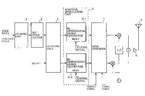
Fig. 4 is a block diagram showing a variable rate
transmission apparatus according to an embodiment 1 of the
present invention. In the drawing, reference numeral 1
11
CA 02262553 1999-O1-29
indicates a framing unit for inputting user data and control data
therein and converting them into frame form, reference numeral
2 indicates an FEC (Forward Error Correction: Error Correction
Coding) and interleaver (signal processing means), reference
numeral 3 indicates a slotting unit (signal processing means), and
reference numeral 4 indicates an adaptive modulation unit
(means for spreading-modulation on data signals in a binary
sequence using bi-orthogonal signals and transmitting the so-
processed signals), which includes, for example, a plurality of bi-
orthogonal signal (Bi-Orthogonal signal: BORT) generator units
4-1 and 4-2 for respectively generating bi-orthogonal signals,
based on Walsh functions, for example, respectively. Reference
numeral 5 indicates a QPSK (Quarternary Phase-Shift Keying:
QPSK) spreader, reference numeral 6 indicates a power amplifier,
and reference numeral 7 indicates an antenna, respectively.
Fig. 5 is a block diagram showing each of the bi-
orthogonal signal generator units 4-1 and 4-2 which constitute
the adaptive modulation unit 4 employed in the variable rate
transmission apparatus according to the embodiment 1 shown in
Fig. 4. In the drawing, reference numeral 21 indicates a
serial/parallel converter (hereinafter called "S/P converter": first
serial/parallel converter), and reference numeral 22 indicates an
orthogonal signal generator for selecting a Walsh function
sequence in accordance with a control signal and selecting and
generating an orthogonal signal according to input data,
12
CA 02262553 1999-O1-29
respectively. Reference numeral 23 indicates an EXOR
(Exclusive OR) circuit for determining the polarity of the
orthogonal signal.
Fig. 6 is a block diagram showing other bi-orthogonal
signal generator units 4-1 and 4-2 which constitute the adaptive
modulation unit 4 employed in the variable rate transmission
apparatus according to the embodiment 1 shown in Fig. 4. Fig. 6
is different from Fig. 5 in that a symbol mapping part 24 exists
between the first S/P converter 21 and the orthogonal signal
generator 22. The symbol mapping part 24 works to enhance the
mapping between input data and bi-orthogonal signals. As a
result, a transmission characteristic can be improved.
Fig. 7 is a block diagram showing a variable rate
transmission apparatus at the time that a data rate of each input
signal is given as 256 kbps (K = 2), Fig. 8 is a block diagram
illustrating a variable rate transmission apparatus at the time
that the data rate of each input signal is equal to 384 kbps (K = 3),
Fig. 9 is a block diagram depicting a variable rate transmission
apparatus at the time that the data rate of each input signal is
equal to 512 kbps (K = 4), and Fig. 10 is a block diagram showing
the variable rate transmission apparatus at the time that the
data rate of each input signal is equal to 128 kbps (K = 1),
respectively. They respectively show equivalent circuits at the
respective data rates, of the variable rate transmission apparatus
according to the embodiment 1. Here, K indicates the number of
13
CA 02262553 1999-O1-29
coded bits (coded data) included in each bi-orthogonal signal.
Fig. 11 is a block diagram showing the details (when K =
4) of the bi-orthogonal signal generator units 4-1 and 4-2 shown
in Fig. 5. In Fig. 11, Fig. 11(a) is a block diagram illustrating the
adaptive modulation units 4-1 and 4-2 shown in Fig. 5, Fig. 11(b)
is an explanatory view showing the relationship between input
information data inputted to the bi-orthogonal signal generator
units 4-1 and 4-2 and output data indicative of bi-orthogonal
signals, and Fig. 11(c) is a block diagram depicting the details of
the bi-orthogonal signal generator units 4-1 and 4-2 respectively
shown in Fig. 5. In the drawing, reference numerals 221
through 223 indicate a logical product circuit (hereinafter called
"AND circuit") respectively, and reference numeral 224 indicates
an EXOR circuit.
The variable rate transmission apparatus according to
the embodiment l, which is shown in Figs. 4 through 11, is a
variable rate transmission apparatus for spreading-modulating
data signals by using a spreading coded sequence and
transmitting the resultant signals therefrom, and transmits data
signals by using bi-orthogonal signals. When the transmission
rate of the data signal is equal to a rate exceeding a
predetermined transmission rate (e.g., 128 kbps), the respective
bi-orthogonal signal generator units 4-1 and 4-2 in the adaptive
modulation unit 4 convert coded data into bi-orthogonal signals in
which Walsh functions have polarities. The resultant outputs
14
CA 02262553 1999-O1-29
are spreading-modulated by the QPSK spreader. Namely, since
bi-orthogonal signals represented in a binary sequence serve so as
to transmit a plurality of coded data, data transmission is
performed efficiently without envelope variation which results in
the case of multi-code multiplexing.
The operation will next be described.
First of all, the framing unit 1 employed in the variable
rate transmission apparatus according to the embodiment 1
shown in Fig. 4 inputs user data and control data each having a
predetermined data transmission rate and outputs them so as to
be delimited at predetermined frame times. The predetermined
data transmission rate may include, for example, 2.4, 4.8, 9.6,
14.4, 16, 19.2, 32, 64, 128, 384, 2048 kbps, etc. Embodiment 1 is
characterized in that when the data rate exceeds 128 kbps, the
data signals are spread and modulated in the binary sequential
state by using bi-orthogonal signals and the data transmission is
executed efficiently.
The FEC interleaver 2 performs error correction coding
and interleaving on the user data and control data outputted
from the framing unit 1. Here, convolutional coding is used for
each frame. After the interleave processing has been executed
by the FEC interleaver 2, the slotting unit 3 divides data into
slots produced in every predetermined period and inserts pilots
into them. Since the framing unit 1, FEC interleaver 2 and
slotting unit 3 are similar to the conventional ones in function
CA 02262553 1999-O1-29
and configuration, their description will not be described here.
The slots with the pilots inserted therein are inputted to
the adaptive modulation unit 4. The adaptive modulation unit 4
selects a Walsh function sequence in accordance with each control
signal according to each of data transmission rates of data whose
data transmission rates exceed 128 kbps, selects a Walsh function
in response to input coded data, and outputs a bi-orthogonal
signal obtained after a polarity operation is executed by each
EXOR. Namely, the control signal serves so as to select K (the
number of coded bits) according to data. The function and
configuration of the adaptive modulation unit 4 will be described
later in detail.
The QPSK spreader 5 inputs therein dual bi-orthogonal
signals having a plurality of coded data information, which are
outputted from the adaptive modulation unit 4 and performs
QPSK spreading-modulation on them using short and long codes.
Since the Cg,IPSK spreader 5 is similar to the conventional one in
function and configuration, its description will not be described
here. The signals QPSK spreading-modulated by the (aPSK
spreader 5 are subjected to QPSK carrier-modulation using
orthogonal carrier waves, after which they are amplified by the
power amplifier 6, followed by transmission to the antenna 7.
Fig. 7 is a block diagram showing the variable rate
transmission apparatus at the time that the data transmission
rate of each input signal is 256 kbps (K = 2). When the
Is
CA 02262553 1999-O1-29
transmission rate of each data sent from the slotting unit 3 is 256
kbps, the S/P converter 21 and orthogonal signal generator 22
provided within the bi-orthogonal signal generator units 4-1 and
4-2 divide input data into two parallel signals and output the
signals. One of them selects either one of W2(0) and W2(1) as a
Walsh function to generate a bi-orthogonal signal. The resultant
orthogonal signal and a polarity signal outputted from the other
of them are inputted to the EXOR circuit 23 from which a bi-
orthogonal signal is outputted.
Fig. 8 is a block diagram showing the variable rate
transmission apparatus at the time that the data rate of each
input signal is 384 kbps (K = 3). When the data rate is 384 kbps,
the S/P converter 21 and orthogonal signal generator 22 provided
within the bi-orthogonal signal generator units 4-1 and 4-2 output
dual input data outputted from the slotting unit 3 as three
parallel signals respectively and select any one of W4(0) through
W4(3) as a Walsh function in two bits to generate a bi-orthogonal
signal. The resultant orthogonal signal and a polarity signal
given in another one bit are inputted to the EXOR circuit 23 from
which a bi-orthogonal signal is outputted.
Fig. 9 is a block diagram showing the variable rate
transmission apparatus at the time that the data rate of each
input signal is 512 kbps (K = 4). When the data rate is 512 kbps,
the S/P converter 21 and orthogonal signal generator 22 provided
within each of the bi-orthogonal signal generator units 4-1 and 4-
17
CA 02262553 1999-O1-29
2 divide dual input data outputted from the slotting unit 3 into
four parallel signals and output them, and select any one of W8(0)
through W8(7) as a Walsh function in three bits to generate a bi-
orthogonal signal. The resultant orthogonal signal and a
polarity signal given in another one bit are inputted to the EXOR
circuit 23 from which a bi-orthogonal signal is outputted.
Fig. 10 is a block diagram showing the variable rate
transmission apparatus at the time that the data rate of each
input signal is 128 kbps (K = 1). Below this data rate, no bi-
orthogonal signal is produced and the data transmission is
intermittently performed using the conventional burst
transmission. Since the configuration and operation in this case
are identical to the conventional one, their description will not be
described. However, when the control signal indicates that the
data rate of each input signal is 128 kbps (K = 1), the S/P
converter 21 allows each input signal to pass therethrough
without performing any operation in the configuration of the bi-
orthogonal signal generator units 4-1 and 4-2 as shown in Fig. 5.
Namely, when the data rate is less than 128 kbps, each of the bi-
orthogonal signal generator units 4-1 and 4-2 is constructed so
that serial/parallel conversion is not performed within the S/P
converter 21 and the output of the orthogonal signal generator 22
is always set to a low level. As a result, the configuration of the
variable rate transmission apparatus can be set to the same
configuration as when the data rates of the input signals shown
is
CA 02262553 1999-O1-29
in Figs. 7 through 9 are respectively 256 kbps (K = 2), 384 kbps
(K = 3) and 512 kbps (K = 4).
A description will next be made of the operations of the
bi-orthogonal signal generator units 4-1 and 4-2 constituting the
adaptive modulation unit 4 employed in the variable rate
transmission apparatus and the variable rate transmitting
method according to the embodiment 1. The respective
operations of the bi-orthogonal signal generator units 4-1 and 4-2
constituting the adaptive modulation unit 4 will be explained
below with respect to the case when the data rate of each input
signal is 512 kbps (K = 4), i.e., the input data is represented in
the form of four input bits (d0 through d3) and one-sequential bi-
orthogonal signal is generated. Since other cases are basically
identical in operation to the following description, the description
thereof will not be described.
The data inputted to the respective bi-orthogonal signal
generator units 4-1 and 4-2 in the adaptive modulation unit 4 are
first converted into 4-bit parallel data (d0, dl, d2 and d3) by the
S/P converters 21 respectively. Next, each of the orthogonal
signal generators 22 generates one orthogonal signal selected
from orthogonal codes indicative of eight (= 2K-1) orthogonal
signals according to 3 (K = 1) bit data (d0, d 1 and d2) of the 4-bit
parallel data, based on the value (= K) of the control signal.
The EXOR circuit 23 performs a multiplying process
between the orthogonal signal obtained from the orthogonal
19
CA 02262553 1999-O1-29
signal generator 22 and the remaining 1-bit data (d3) of the 4-bit
parallel data to execute a polarity operation, thereby generating a
bi-orthogonal signal and thereafter outputting it to the outside.
In the variable rate transmission method and variable
rate transmission apparatus according to the embodiment l,
Walsh function coded sequences are used to obtain orthogonal
signals. In this case, Walsh function sequences W8(n) (where n
= 0 to 7) shown in Fig. 11(b) are outputted as orthogonal signals,
based on the 4-bit parallel data d0 through d3. Namely, since
one function sequence can be selected from the values of the three
bits (d0, dl and d2) in the 4-bit parallel data, eight kinds of Walsh
function sequences whose each sequence length is represented as
8, are produced. Reference numeral W8 indicates a Walsh
function whose sequential length is 8. Numerals 0 through 7
inside the parentheses indicate function numbers. Each Walsh
function sequence selected as an orthogonal signal is inverted or
non-inverted in accordance with the value of the remaining 1-bit
data (d3) of the 4-bit parallel data, and the result thereof is
outputted as a bi-orthogonal signal. Thus, the bi-orthogonal
signal comprises a coded sequence whose sequence length is 8
and includes 4-bit information.
Incidentally, the inversion and non-inversion of each
digital value is performed by an exclusive OR gate in the case of
binary representation in the form of 0 and 1 and carried out by a
multiplier in the case of + 1
CA 02262553 1999-O1-29
and -1. In the present embodiment, the inversion and non-
inversion of each digital value will be described using the binary
representation of 0 and 1. In the following description, the
duration from the beginning of the Walsh function sequence to
the end thereof will be called a "cycle", the interval between codes
constituting the Walsh function will be called a "code interval",
and the inverse of the code interval will be referred to as a "code
rate".
When the Walsh function is used as the orthogonal
signal, an orthogonal signal generator 22 shown in Fig. 11(c)
comprises AND circuits 221 through 223 for taking AND logic
between clocks 225, 226 and 227 respectively having rates of 1/2,
1/4 and 1/8 of the code rate (= 1/Tmc, Tmc: code interval) with
input data d0, dl and d2, and an EXOR circuit 224 for XORing
the outputs of the three AND circuits 221 through 223. The
clocks for the code rate are essential to the configuration of
hardware. The clocks respectively having rates 1/2, 1/4 and 1/8
of the code rate are basic clocks produced by a divider circuit such
as a counter or the like.
The orthogonal signal generator 22 can selectively choose
a Walsh function so as to generate an orthogonal signal. The
Walsh functions are defined as row vectors of a Hadamard matrix
H (N) with 2K rows x 2K columns and are expanded by increasing
the degrees from [H(N/2), H(N/2)] obtained by repeating a
Hadamard matrix H (N/2) with 2K -1 rows x 2K -1 columns and
21
CA 02262553 1999-O1-29
[H(N/2), H ~k (N/2)] obtained by inverting and repeating the
Hadamard matrix. Here, symbol >k indicates an inverted
matrix.
H1 is used as the reference. A first row is represented
as [0, 0] and a second row is represented as [0, 1], and they
correspond to W2(0) and W2(1) respectively. H2 are created as
[H 1, H 1] and [H 1, H ~k 1] from H 1. As a result, four row vectors
of [0000], [0101], [0011] and [0110] are obtained and correspond to
W4(0) through W4(3) respectively. W8(0) through W8(7), created
by a method similar to the above, are illustrated in Fig. 11(b).
When W8(0) and W8(1), W8(2) and W8(3), W8(4) and W8(5), and
W8(6) and W8(7) are compared with one another, odd-numbered
bits as viewed from the least significant bit and the immediately
following even-numbered bits are classified as similar or inverted.
Similar ones include W8(0), W8(2), W8(4) and W8(6),
whereas inverted ones include W8(1), W8(3), W8(5) and W8(7).
The decision as to whether they are similar or inverted,
corresponds to the value of the least significant bit d0 of the data
shown in Fig. 11(b). Namely, if the least significant bit d0 is 0,
then they are regarded as the same. If the least significant bit
d0 is 1, then they are regarded as inverted. Inversion for each
bit is implemented by the clock 225 having a rate equal to one-
half the code rate. Whether this should be adopted, depends on
the least significant bit d0 and is implemented through the AND
circuit 221 used as the logical product circuit.
22
CA 02262553 1999-O1-29
When W8(0) through W8(7) are divided into four pairs by
2 bits from the least significant bit, W8(0) and W8(2), W8(1) and
W8(3), W8(4) and W8(6), and W8(5) and W8(7) are respectively
compared with one another. As a result, W8(0), W8(1), W8(4)
and W8(5) are identical as regards double bit and repeated,
whereas in the case of W8(2), W8(3), W8(6), and W8(7), respective
double bits are inverted and repeated. A decision as to whether
the bits are the same or inverted, corresponds to the value of the
second bit dl of the data shown in Fig. 11(b). Namely, if the
second bit dl is 0, then they are regarded as the same. If the
second bit d1 is 1, then they are regarded as inverted. Inversion
in 2-bit units is implemented by the clock 226 having a rate equal
to one-fourth the code rate. Whether this should be adopted,
depends on the second bit dl and is achieved through the AND
circuit 222 which corresponds to the logical product circuit.
Whether sequences set by 4 bits from the least
significant bit are the same and continuous or inverted and
continuous, is associated with the polarity of the third bit d2.
Inversion of the sequences set every 4 bits is implemented by the
clock 227 having the rate equal to one-eighth the code rate.
Whether this should be adopted, is dependent on the third bit d2
and is achieved through the AND circuit 223 which corresponds
to the logical product circuit.
When the inversion or non-inversion results in three bit
intervals are caused to pass through the EXOR circuit 224, a
23
CA 02262553 1999-O1-29
sequence containing the results is obtained as a Walsh function.
Thus, each Walsh function sequence, which depends on the input
data bit d0, d1 and d2, i.e., which is selected from d0, dl and d2,
is outputted as an orthogonal signal from the EXOR circuit 224.
Thus, since the orthogonal signal generator 22 can
generate specific orthogonal signals only by the simple generating
mechanism of the clocks and the input data, a transmitter having
the function of being capable of maintaining a linear
characteristic of a power amplifier in a simple hardware
configuration can be implemented if this is incorporated therein.
Further, since each orthogonal signal is easy to produce, the
generation of the bi-orthogonal signal from each of the bi-
orthogonal signal generator units 4-1 and 4-2 can be easily
implemented. While a receiver needs the operation of
demodulating each bi-orthogonal signal, fast Hadamard
transformer (Fast Hadamard Transformer: FHT) is performed
where the Walsh function is used as the orthogonal signal on the
transmitter side. Thus, since the demodulating process can be
easily executed, the receiver can be constructed in a simple
hardware configuration and hence the demodulating process can
be easily carried out.
The operation of each bi-orthogonal signal generator unit
configured so as to have the symbol mapping part 24 as shown in
Fig. 6 will be explained using Fig. 12. As shown in Fig. 12(a),
the symbol mapping part 24 performs EXOR logic between a
24
CA 02262553 1999-O1-29
polarity bit d3 and other input data d0, dl and d2 and thereafter
inputs the EXOR-computed data to an orthogonal signal
generator 22. As a result, d'0, d'2 and d'3 are inputted to the
orthogonal signal generator 22. The relationship between the
input data d0, dl, d2 and d3 and the bi-orthogonal signals is
shown in Fig. 12(b). Symbol mapping in this case means that
the input bits having inversion relation to one another are
assigned to the bi-orthogonal signals identical in orthogonal
function to each other and different in polarity from each other.
Namely, (0, 0, 0, 0) and (1, 1, 1, 1) respectively indicative of (d0,
d1, d2, d3) are assigned to W8(0) and -W8(0) respectively.
Similarly, (0, 0, 0, 1) and (1, 1, 1, 0) are respectively assigned to
W8(1) and -W8(1). Since the distance between the bi-orthogonal
signals identical in orthogonal function to each other and
different in code from each other is greater than the signal
distance between the orthogonal functions, the probability that
an error will take place between the signals identical in
orthogonal function to each other and different in polarity from
each other, is minimized. Namely, the probability that all the
bits will be mistakenly demodulated upon demodulation, can be
minimized by performing such mapping.
Although the orthogonal signal generator 22 for selecting
and outputting each Walsh function as the orthogonal signal is
used to obtain each bi-orthogonal signal in the above-described
examples, the variable rate transmission apparatus and variable
CA 02262553 1999-O1-29
rate transmission apparatus according to the present invention
are not limited to this. For example, an orthogonal gold signal
sequence or the like may be used as the orthogonal function in
place of the Walsh function.
According to the embodiment 1 as described above,
after a series of signal processes such as error correction coding,
etc. has been carried out, serial/parallel transformation is
performed on fast data exceeding a predetermined data rate so as
to convert it to a bi-orthogonal signal. It is then transmitted, as
it is, in a binary sequence. Namely, since data signals are
spreading-modulated and transmitted in a binary sequence by
using the bi-orthogonal signals in the case of the transmission of
each signal at a data rate exceeding a basic rate, the linear
characteristic of the power amplifier 6 can be maintained even in
the case of a fast data rate. Further, no interference is given to
adjacent frequency bands and high-quality data transmission can
be performed. Since Walsh functions are used, hardware
configuration is easy and a demodulating process can be also
implemented in a simple configuration. Since the bi-orthogonal
signal transmission is excellent as regards error-rate
characteristics, data error-rate characteristics can be improved
and higher-quality data transmission can be achieved.
Embodiment 2:
The variable rate transmitting method and variable rate
transmission apparatus according to the embodiment 1 shown in
zs
CA 02262553 1999-O1-29
Figs. 4 through 11 show the case in which after a series of signal
processes such as error correction coding, etc. has been carried
out, serial/parallel transformation is performed to generate each
bi-orthogonal signal, and thereafter a plurality of signal
sequences are transmitted. However, a method is also
considered wherein when a signal transmitting process at a fast
rate is performed, a series of signal processes such as error
correction coding, etc. is performed after the serial/parallel
transformation is first carried out. A description will be made of
a case in which in a variable rate transmitting method and a
variable rate transmission apparatus according to an embodiment
2 to be described below. A series of signal processes such as
error correction coding, etc. is performed after each input signal
given at a fast data rate is first transformed into serial/parallel
form, to thereby generate each bi-orthogonal signal without using
a multicode. Hence fast data is transmitted while remaining
held in a binary sequence.
Fig. 13 is a block diagram showing the variable rate
transmission apparatus according to the embodiment 2 of the
present invention. In the drawing, reference numeral 80
indicates a serial/parallel converter (hereinafter called "SIP
converter": second S/P converter) which converts data signals of
user data and control data into a plurality of parallel signals.
Reference numeral 81 indicates each forward error correcting
unit (Forward Error Correcting Unit: FEC unit, signal processing
27
CA 02262553 1999-O1-29
means), which performs a series of processes such as an error
correction coding (convolutional coding) process, an interleaving
process and a framing process with the insertion of pilot symbols
and CRC therein, etc. Reference numeral 4 indicates an
adaptive modulation unit and reference numeral 5 indicates a
QPSK spreader. Since these are identical to those employed in
the variable rate transmission apparatus according to the
embodiment 1 shown in Figs. 4 through 10, they are identified by
the same reference numerals and their description will not be
described again.
Figs. 14 through 17 show the case in which data rates of
input signals are respectively 128 kbps, 256 kbps, 384 kbps and
512 kbps, and are respectively block diagrams each showing the
configuration of the variable rate transmission apparatus
according to embodiment 2 shown in Fig. 13.
The operation will next be described.
The S/P converter 80 inputs input signals each having a
fast data rate therein and converts them into parallel data
signals. The FEC units 81 input the four maximum parallel
data signals converted by the S/P converter 80 therein and
perform a series of processes such as an error correction coding
process, convolution coding process, an interleave process and a
framing process with the insertion of pilot symbols and CRC
therein, etc. on the signals. Parallel data signals outputted from
the respective FEC units 81 are inputted to the inside of the
28
CA 02262553 1999-O1-29
adaptive modulation unit 4 employed in the variable rate
transmission apparatus according to the embodiment 1. Since
the subsequent operations are just the same as those of the
adaptive modulation unit 4 and the QPSK spreader 5 employed in
the variable rate transmission apparatus according to the
embodiment 1 shown in Figs. 4 through 10, their description will
not be described.
In the variable rate transmission method and variable
rate transmission apparatus according to embodiment 2 as
described above, data signals are first converted into
serial/parallel form and a series of signal processes such as error
correction coding, etc. is effected on the resultant parallel data
signals to thereby generate bi-orthogonal signals without having
to use a multicode, after which a plurality of signal sequences are
transmitted.
According to embodiment 2, as has been described above,
input signals sent at a fast data rate are first converted into
serial/parallel form and are then separated into a plurality of
spreading code channels. Thereafter, a series of signal processes
such as error correction coding, etc. is effected to thereby generate
bi-orthogonal signals without having to use a multicode, after
which a plurality of signal sequences are transmitted. Thus,
since data signals are spreading-modulated and transmitted in a
binary sequential state by using bi-orthogonal signals obtained by
Walsh functions at symbol spreading portions in the case of the
29
CA 02262553 1999-O1-29
transmission of each individual signals at a data rate exceeding a
basic rate in a manner similar to the embodiment 1, a linear
characteristic of a power amplifier 6 can be maintained even in
the case of a fast data rate. Further, little interference is given
to adjacent frequency bands and high-quality data transmission
can be performed. Since Walsh functions are used, the
configuration of hardware is easy and a demodulating process can
be also implemented in a simple configuration. Since the bi-
orthogonal signals are generated using Walsh functions, data
error-rate characteristics are improved and higher-quality data
transmission can be carried out. Incidentally, the QPSK
spreader is used for spreading modulation in the present
embodiment. Although the bi-orthogonal signals are dual-
inputted in this case, an envelope variation is not produced in a
manner similar to the normal QPSK.
INDUSTRIAL APPLICABILITY
As described above, the variable rate transmission
method and variable rate transmission apparatus according to
the present invention is suitable for holding a linear
characteristic of a power amplifier and transmitting high-quality
data even if a data rate is high.