Note: Descriptions are shown in the official language in which they were submitted.
CA 02262607 1999-01-29
WO 98/05134 PCT/hP97/04090
"BIDIRECTIONAL MULTICHANNEL OPTICAL TELECOMMUNICATION
SYSTEM"
DESCRIPTION
It is an object of the present invention to provide a bidirectional multichanneltelecommunication system, a bidirectional optical amplifier, and a method for the
bidirectional transmission of optical signals.
In the latest telecommunication technology, it is known to use optical fibers
to send optical signals carrying info~ d~io,, for long-distance communication.
It is also known that optical signals sent in an optical fiber undergo
attenuation along the way, making it necessary to amplify the signal so that it will
travel the entire required distance and reach the receiving station at a power
level sufficient for correct signai reception.
Said amplification may be effected by means of appropriate amplifiers
placed at predetermined intervals along the line, which periodically boost the
power of the transmitted optical signal.
Optical amplifiers are suitably used for this purpose, by which the signal is
amplified while remaining in optical form, i.e. without the optoelectronic detection
and electrooptical regeneration of same.
Said optical amplifiers are based on the properties of a fluorescent dopant
(e.g. erbium) which, if appropriately excited by the application of luminous
energy, provides a strong emission in the wavelength band corlesponding to the
minimum attenuation of light in siiica-based optical fibers.
Said amplifiers are unidirectional devices, i.e. having a predetermined
direction of travel of the optical signal inside them.
This is due, as described for example in US patents 5,204,923 and
5,210,808 of the Applicant, to the fact that the optical amplifiers, particularly if
high gain values are required, incorporate unidirectional components that
prevent signals reflected outside the amplifiers, e.g. due to Rayleigh scattering
along the optical line fibers connected to the amplifiers, from returning into the
amplifier, causing interferometric noise.
CA 02262607 1999-01-29
WO 98/05134 PCT/EP97/04090
For the bidirectional ~,ans~n.ssion of optical signals, known technology
generally calls for the use of two separate communication lines, equipped with
their respective amplifiers, each of which is used to communicate in a single
direction. This results in a high connection cost.
Nevertheless, some technologies are know whose objective is to permit
bidirectional tra-,smissiG,- on fiber-optic lines by means of bidirectional optical
amplifiers.
Bidirectional amplification schemes have been presented with the use of a
single unidirectional amplifier that exploit the possibility of fluorescent doped
amplifiers to independently amplify signals at different wavelengths.
A bidirectional amplifier based on this principal is described in the article byS. Seikai et al.: "Novel Optical Circuit Suitable for Wavelength Division
Bidirectional Optical amplification", published in Electronics Letters, vol. 29, no.
14, 8 July 93, pages 1268-1270. It discusses a device placed along a fiber-optictra"sr"ission line in which two signals with different wavelengths prop~te in
opposite dire-;tions and which consists of wa\rele.lylll selective couplers and a
known type of unidir~ctional doped-fiber amplification unit connected by sections
of passive optical fiber. The wavelengths of the signals are both internal to
amplification band of the doped fiber. By means of selective couplers the two
signals at different wavelengths are input to different optical paths. The two
optical paths coincide only in the section corresponding to the amplifying fiber,
which is p~ssed through by the two signals in the same direction. The device hasa problem of instability G~used by internal reflections at a wavelength between
those of the propagating signals, a problem resolved through the addition of
filters, some of them adjustable, which results in a highly complic~ted structure
and the need to use devices to accurately and continuous adjust said filters.
Patent arpli~lion EP96100586, filed on 17 January 1996 in the name of
the Applicant, desc-ibes, among other things, a bidirectional optical amplifier
comprising:
- an optical amplification unit including at least an optical isolator,
- two optical input and output ports for at least two optical signals having
opposite propagation directions, said sigr~als having, respectively, a first and a
CA 02262607 1999-01-29
W O 98/05134 PCTAEP97/04090
second distinctwa~ele.,gtlls,
- two first and two second wavelength selective optical couplers, having
respectively a first wavelength r)~ssh~nd, including said first wavelength, and a
second wavele. Iyll, passband, including said second wavelength; with no
5 overlapping,
said amplification unit being connected between two opposite nodes of an
optical bridge circuit, to whose other opposite nodes said input and output ports
are connected, and said first and second selective optical couplers being present
at the nodes of said bridge circuit, in which said first and second selective
10 co~pl~rs are a"anged sy",n,ellically with respect to the amplification unit and
with respect to the input and output ports of said optical signals.
Bidirectional a",,c llrlcdlion schemes have also been presented with
separation of the counterpropagating signals and the use of a unidirectional
amplifier for each dir~diGn.
As an example, the article by C.W. Barnard et al. "Bidirectional Fiber
A,nplifier~", published in IEEE rhotonics Technology Letters, vol. 4, no. 8,
August 1992, pages 911-913, descriLes bidirectional erbium-doped fiber
a""Jl;r,er repeaters for bidirectional fiber networks and OTDR fault detection. At
each repeater the counterpropagating signals are separated, amplified
20 separately, then recombined. Signal separation is done by a bidirectional fiber
coupler or an optical circulator. According to the authors, for example, one
pr~pagdtion direction could be assigned 1525-1535 nm, the other could be
assigned 1550-1560 nm, and the OTDR wavelength could be 1548 nm.
Optical teleco",r"unication systems are known with wavelenylll division
25 multiplexing (WDM) l,dns",ission. In these systems, a number of channels are
sent, i.e. a number of mutually independent transmission signals, on the same
line, usually consisling of an optical fiber, by means of optical wavele.,gtl,
multiplexing. The l,ans"litled channels can be either digital or analog and are
mutually dislinguished bec~use each of them is ~ssociated with a specific
30 wavelength.
US patent 5,283,686, in the name of D.R. Huber, describes, among others,
optical systems including an optical amplifier and a narrow-bandwidth optical
CA 02262607 1999-01-29 ,- -'
PC693
filter for removing undesired spontaneous emission. An in-fiber Bragg grating reflector
reflects substantially only the input amplified signal back to an optical circulator port. The
undesired emission exits from the grating reflector and is removed from the system.
Cascaded grating reflectors are used in a wavelength division multiplexing (WDM) system.
The article of K.Y. Chen et al., UDemonstration of in service supervisory repeaterless bi-
directional wavelength division multiplexing transmission systemn, vol. 7, no. 9, 1
September 1995, states that repeaterless long distance fiber transmission systems using
erbium doped fiber amplifiers as a transmitter power amplifier and/or as a receiver
preamplifier have many applications, in which cases it is infeasible or impossible to have
10 an in line amplifier, such as island hopping and intracity links. In this letter, an in service
supervisory repeaterless bi-directional six WDM channel transmission over a 200 Km
single fiber link is demonstrated.
The patent application EP 0 535 590 discloses a two way repeater apparatus for directly
amplifying optical signals, to be transmitted in mutually opposite directions. Said repeater
receives an outward input optical signal S1 of 1.552 microns in wavelength at aninpuVoutput terminal 1, and receives an inward optical signal S1r of 1.536 microns in
wavelength at an inpuVoutput terminal 20.
The patent application DE 36 32 047 A discloses a communication system used for digital
narrow band and wideband signals transmitted in both directions via a single optical
20 waveguide.
The article of M.J. Chawki et al., UEvaluation of an optical boosted add/drop multiplexer
OBADM including circulators and fiber grating filters", proceeding of ECOC, vol. 1, 17
September 1995, discloses two OBADM configurations wherein bi-directional EDFA and
fiber grating filters are placed between the 2 circulators.
25 The patent application EP 0 729 248, corresponding to the patent US 5,633,741, discloses
that WDM optical fiber communications entails bi-directional transmission with at least two
WDM channels in opposite transmission directions in a singlefiber. Communication is by a
single fiber transmission line served by bi-directional amplifiers. The amplifier includes
fiber gratings that serve as hlters and st~hi'i~e against oscillation due to reflections and to
30 Rayleigh back scattering.
Al\~ENDED SHEET
CA 02262607 1999-01-29
PC693 4a
It is known that the wavelength bandwidth available for signals, in optical
communication systems with doped-fiber amplihers, is limited by the characteristics of
the active dopant used. In the case of amplifiers doped with erbium, for example, said
bandwidth is limited to the wavelength bandwidth included approximately between
1530 and 1565 nm.
The Applicant has observed that the known WDM communication systems are
further limited regarding the number of channels, i.e. the independent wavelengths
usable for transmission within said amplification bandwidth.
The need to reduce noise, particularly of the interferometric type, associated with
l~ the retroreflection of signals or noise toward the amplifiers, makes it imperative to
maintain a good isolation between the channels at the various wavelengths
propagating in the system, i.e. a good suppression of radiation at intermediate
wavelengths between those of the communication channels. This isolation may be
obtained, in known systems, only by maintaining a channel separation greater than a
l5 predetermined minimum value, which limits the number of channels usable in the
available wavelength bandwidth. This minimum value depends on the characteristics
of the components employed in the system, such as the spectral characteristics of the
wavelength selective components (e.g. bandwidth, center-band attenuation, figure of
merit) and wavelength stability (thermal and temporal) of the filters and of the optical
20 signal sources.
Furthermore, to separate signals with different wavelengths, e.g. to drop some of
them to receivers placed in intermediate amplification nodes or to send them, at the
receiving station, to separate receivers, contiguous channels (in terms of wavelength)
must be separated by more than a predetermined limit value.
Said limit value depends primarily on the characteristics of the wavelength
AMEI~IDFO Sli~E,
CA 02262607 1999-01-29
W O 98/05134 PCT~EP97/04090
selective components employed along the optical signal path.
By means of the present invention it is possible to transmit in an optical
telecommunication system a number of independent optical channels greater
than is permitted by known techniques, by employing wavelen~tlr selective
5 col"po"ents of equal characteristics.
The Applical ll has found that by feeding wavelength-contiguous channels in
two opposite directions in the system it is possible to use filtering, multiplexing
and demultiplexing means having spectral resolution greater than the spacing
between the channels.
10 According to a first aspect, the present invention concerns a bidirectional
multichannel optical telecommunication system comprising:
- means for generating optical signals suitable for generating at least three
optical signals having, respectively, a first, a second and a third mutually distinct
wavelengths;
15 - a line for transmitting optical signals;
- means for inputting said first and third optical signals to said transmission
line, placed at a first end of said tra~,s~"ission line;
- means for inputting said second optical signal to said l~ans~ission line,
placed at a second end of said transmission line opposite from said first end;
20 characterized by the fact that the value of said second wavelength is comprised
between said first and third wavelengths.
According to another ~spect. the present invention regards a multichannel
optical telecommunication system for trans",illing optical signals comprising:
- a fiber-optic line having a first and a second end;
25 - means for inputting, at said first end of said line, first optical signals
propa~~ali"9 in a first di,ection and having a first series of mutually distinctwavelengths;
- means for inputting, at said second end of said line, second optical signals
propagating in a second direction, opposite to said first direction, and having a
30 second series of wavelengths mutually distinct and distinct from the wavelengths
of said first optical signals;
- first means for demultiplexing said optical signals, at said second end of
CA 02262607 1999-01-29
WO 98/05134 PCT/EP97/04090
said line, and second means for demultiplexing optical siynals at said first end of
said line, said first and said second means of demultirl~xing being suitable fordemultiplexing signals distant from each other in wavele,lylll by a quantity
greater than or equal to a predetermined minimum value.
5 characterized by the fact that the wavele.~ylhs of said first signals differ from
each other by a quantity greater than or equal to said minimum value, the
wavelengths of said second signals differ from each other by a quantity greater
than or equal to said minimum value, while the wavelenylhs of said first signalsdiffer from the wavelengths of said second signals by a quantity greater than or10 equal to half said minimum value.
In one of its versions, said system comprises bidirectional amplification means
optically connected along said fiber-optic line. Preferdbly, said means comprise:
- means for separating said first signals from said second signals;
- means for amplifying said first signals;
15 - means for amplifying said second signals;
- means for combining said first and second signals.
Said means for separating and said means for combining include respective
optical circulators.
Said means for amplif,ving said first and second signals may be unidirectional
20 and may comprise respective comb filters sl~iP~lc for l,ans",itting signals at
wavelengths within bands including the wavelengths of said first and said secondsignals, r~specti-/ely, and suitable to attenuate r~di~tion at wavele-~ths external
to said bands. Said comb filters may col,lprise an optical circulator and Bragg
grating reflectors c~sc~ded at an inle""ediale port of said circulator.
25 In one version of said system, said minimum distance value is less than or equal
to 1 nm.
According to a third ~spect, the present invention r~gards a multichannel optical
telecomm~",i~lio" system forthe l,ans,nission of optical signals comprising:
- a fiber-optic line;
30 - multiplexing and demu'tirlexing means, for adding and dropping, in at leasttwo different positions along said line, optical signals having mutually distinct
wavelengths, said multiplexing and demultiplexing means having a spectral
CA 02262607 1999-01-29
WO 98/05134 PCT/EP97/04090
resolution y~aler than the minimum spacing between channels,
characterized by the fact that channels contiguous in wavelength are fed in
opposite directions along said line.
According to a fourth aspect, the present invention regards a bidirectional optical
5 amplifier comprising:
- means for inputting first optical signals plO~ agaling in a first direction and
having a first series of mutually distinct wavelengths;
- means for inputting second optical signals prop~g~ting in a second
direction, opposite said first direction, and having a second series of
10 wavelengths, mutually distinct and distinct from the wavelengths of said first
optical signals;
- means for separating said first optical signals from said second optical
signals;
- means for amplifying said first signals;
15 - means for amplifying said second signals;
- means for combining said first and said second signals;
cha~cleri~ed by the fact that the wavelengths of said first and said second
signals are mutually staggered.
Said means for separating and said means for combining advantageously
20 comprise respective optical circulators.
Said means for amplifying said first and second signals may be unidirectional
and may incl~des respecti~e comb filters suitable for transmitting signals at
wavelengths within bands comprising the respective wavelengths of said first
and said second signals and suitable for attenuating radiation at wavelengths
25 external to said bands. Said comb filters may comprise an optical circulator and
Bragg grating reflectors c~sc~ded at an inlel",ediate port of said circulator.
According to a fifth aspect, the present invention regards a method for the
bidirectional ll..nsll.issio,) of optical signals along an optical communicalion line
comprising the steps of:
30 - generating first optical signals at a first series of wavelengths;
- generating second signals at a second series of wavelengths, dirrer~nl from
the wavelengths of said first series;
CA 02262607 1999-01-29
WO 98/05134 PCTIEP97/04090
- trans,r,illi.,g said first siyt~als in a first direction along the optical
~lecon""unic~tion line;
- tra"sn,itli"g said second signals in a second direction along the optical
telecon,munication line;
5 in which the wavelengths of said first signals are staggered with respect to the
wavelengths of said second signals.
In one version said method comprises the step of amplifying said first and said
second signals along the optical communication line which in turn preferably
comprises the steps of:
10 - separating said first from said second signals;
- amplifying said first signals by means of a first optical amplifier;
- amplifying said second signals by means of a second optical amplifier;
- recombining said first and said second signals along said
telecommunication line.
Additional information may be derived from the following desc,i~ulion with
,erere"ce to the attached drawings showing:
in fig. 1 diagram of an optical telecommunication system;
in fig. 2 diagram of a transmission interfacing unit;
in fig. 3 diagram of an optical power amplifier;
in fig. 4 diagram of an optical preamplifier;
in fig. 5A diagram of an optical demultiplexer;
in fig. 5B diagram of a wavelength-selective optical splitter;
in fig. 6 diagram of a bidirectional optical amplifier
in fig. 7 diagram of an optical amplifier associated with a device of a first
type for adding and dropping signals;
infig. 8 diagram of an optical amplifier associated with a device of a
second type for adding and dropping signals.
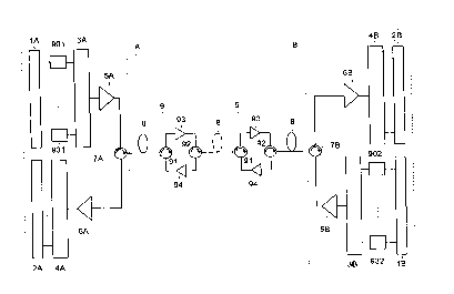
As shown in figure 1 a bidirectional optical telecommunication system with
wavelength-division multiplexing according to the present invention comprises
30 two terminal stations A and B each of which includes a respective transmission
station 1A 1B and a respective receiving station 2A 2B.
CA 02262607 1999-01-29
W O98/05134 PCT~EP97/04090
In particular, in the version shown in the figure, trans",ission station 1A
comprises 16 optical signaJ transrr,itlers with a first series of wavelengths,
indicated with odd-numbered subscli~Jls, ~ 3~ 31 (incluclecl, for example,
in the wavelel,yll, band of 1530-1565 nm) and l-~ns~ission station 1B
5 comprises 16 optical l,dns,nillers with a second series of wavelengths, indic~ted
with even-numbered subscripts, ~2. ~.------~32-
The wavelengths of the second series are selected so that they arestaggered with respect to the wavelengths in the first series.
In other words, each pair of wavelengths of one series encomr~sses a
10 wavelength of the other series.
In the present case, the wavelengths of the two series will be indicated as
staggered, more generally, even when the wavelengths of the signals of each of
said series, corresponding to optical signals emitled by one of the transmissionstations 1A, 1B and prop~g~ting in the system in one of the two directions, are
15 separated (in frequency) by a quantity greater than or equal to 2D, where D
ind.cales the minimum bandwidth (in frequency) of the wavele"~tl~ selective
components used in the system to separate the signals at the various
wavelengths.
The number of independent wavelengths used for the signals for each
20 transmission station is not limited to the value of 16 indicated in the device
desclibed and may assume a different value. The number of wavelengths,
collespGIldil)g to the number of optical cha~nels used for llansll,;ssio" in each
direction, may be selected in relation to the c har~cltri~lics of the
telecommuni~liG" system. In particular, in a telecommunication system
25 according to the present invention, it is possible, after the system
implemenlaliol" to i"cr~:ase the number of channels to increase the trans",illi"g
car~city of the system, e.g. to accol""~odate an increased traffc demand, as will
be indicated below.
The waveler,yll,s may be selected so that the corresponding frequencies are
30 equally sp~cerl within the available spectral alnplificdlion band, so as to utilize
said band efficiently.
CA 02262607 1999-01-29
W O 98/05134 PCT~EP97/04090
It is possible, however, for the frequencies to be totally or partially unequally
spaced, e.g. so as to reduce the effect of non-linear phenomena, such as four
wave mixing (FWI\/I) in optical fibers used for l,ar,smilli"g the signals.
The useful amplirlcdliol1 band of the amplifiers may also be constituted of two
5 or more dislil)ct spe.;t~dl bands separated by spectral bands not well-suited for
signal trans",issiol- or amplification, e.g. due to the particular spectral
cha,acleri:,lics of the amplifiers or optical fibers employed in the
telecommunication system. In this case, the wavelengths of the communication
channels may, for example, be selected such that the cGnesponding frequencies
10 are equally spaced within each individual spectral band, with the separation
between ~djacellt channels propagating in the same direction greater than or
equal (in frequency) to twice said value D.
As an example, the waveler,ylhs may assume values between about 1535
nm and about 1561 nm, where consecutive wavelengths, in ascending order, are
used all~r~,at~ly for each of the two series ~ 3,-----~ ~31 and ~. ~4------- ~32-
The spacing between the 32 total wavele. I~tl ,s, in this case, is about 0.8 nm.The optical transmitters comprised in llans",ission stdtiGns 1A and 1B are
modulated, directly or with external modul~tion, according to system
requirements, in particular in relation with the chromatic dispersion of the optical
20 fibers in the system, with their lengths, and with the intended lldns,~,ission
velocity.
The outputs of each transmitter of tr~"smission statio"s 1A and 1B are
connected to multiplexers 3A and 3B, resrectively, which combine their optical
signals each toward a single output, connet;ted r~specti~/ely to the input of
25 optical power amplifiers 5A and 5B. The outputs of these al"~ ers are
connected to an input port of optical circulators 7A and 7B.
An intermediate port of optical circulators 7A and 7B is connected to one end
of an optical line 8, which connects the two terminal slalions A and B together.The optical fiber of optical line 8 is normally a single-mode optical fiber of the
30 step index or dispersion shifted type, conveniently incl~.lclet~ in a suitable optical
cable, and has tens (or hundreds) of kilometers of length between each
CA 02262607 1999-01-29
WO 98/05134 PCT/EP97/04090
11
amplifier, up to the desired connection distance.
Inserted along line 8 are bidil~cliGI)al optical amplifiers 9. Each of them
comprises two optical circulators 91 and 92 and two optical amplifiers 93 and 94,
which will be described further on. A central port of each optical circulator is5 connected to the optical fiber of line 8, e.g. through an optical connector, and
acts as an inpuVoutput port for the bidirectio~al amplifier. Optical amplifier 93 is
optically connected between an output port of optical circulator 91 and an inputport of optical circulator 92. Optical amplifier 94 is optically connected between
an output port of optical circulator 92 and an input port of optical circulator 91.
10 Although figure 1 indicates two bidirectional optical amplifiers 9, there may be
one or more bidirectional optical amplifiers in suGcession, depending on the
overall length of the optical connection and the power in the various sections of
it. A fiber section between a terminal station and an amplifier, for example, orbehNeen two sl ~ccessive dl "~,lifier~, may be on the order of 100 kilometers long.
15 Receiving :.L-dliol)s 2A and 2B are connected to the output ports of optical
circulators 7A and 7B through pr~sn~plifiers 6A and 6B and demultiplexers 4A
and 4B.
The optical circulators are passive optical components, co,l,-l-only equipped
with three or four access ports placed in an ordered sequence. After defining a
20 first arbitrarily chosen ~ccess port as uinput port", the next ports in sequence will
be inclicaled as central port and output port. The optical circulators lldllsl"il
unidireotiGnc.lly the radiation input by each of the ports to one only of the other
ports, namely the next one in sequence. The circulators used in the present
invention are preferdbly of the poldri~aliGn-indepel)del)t type.
25 Preamplifier, in the col1texl of the present invention, is an amplifier
dimensioned to cGInpensate the losses of the last se~liGn of optical line and the
insertion losses of demultiplexer 4A or 4B, so that the power level of the signal
input to the r~csivcr is suited to the sensitivity of the device. It is also the task of
the preamplifier to limit signal dy.-al--.~s, reducing the power level varidlio"s of
30 the signals at the receiv0r input with respect to the power level variation of the
signals from the transmission line.
CA 02262607 l999-0l-29
PC693 12
Demultiplexers 4A and 4B arè suited for taking 16 signals overlapped in a singleinput port connected to the output of preamplifier 6A, 6B and separating them onto 16 optical fibers, in accordance with their respective wavelengths.
When the optical signals for transmission are generated by signal sources with
their own transmission characteristics (such as wavelength, modulation type,
power) different from those envisaged for the described link, each transmission
station 1A, 1B comprises interfacing units 901, 903, ..., 931 and 902, 904, ..., 932,
respectively, for receiving the optical signals generated by transmission stations
1A, 1B, detecting them, regenerating them with new characteristics suited to theo transmission system and sending them to multiplexers 3A, 3B.
In particular, said interfacing units generate optical working signals with
wavelengths ~" ~, .... , ~31 and ~21 ~41-----1 ~32- respectively, suited to the system
requirements as described below.
US patent 5,267,073 by this same Applicant, describes interfacing units
comprising in particular a transmission adaptor for converting an optical input
signal into a form well-suited for the optical transmission line and a receptionadaptor for converting the transmitted signal into a form well-suited for a reception
unit.
For use in the system of the present invention, the transmission adaptor
comprises, preferably, an externally modulated laser as an output signal
generation source.
The diagram of a transmission interfacing unit 900, of the type well-suited for
use within the context of this invention, is shown in figure 2 in which, for the sake
of clarity, the optical connections are represented by solid lines, while the
electrical connections are represented by broken lines.
The optical signal, coming from an external source 207, is received by a
photodetector (photodiode) 208, which emits an electrical signal which is fed to an
electronic amplifier 209.
The electrical signal output by amplifier 209 is fed to a circuit 210 that
drives a modulable laser emitter, designated overall as 211, that generates an
optical
~MENDED SHEET
CA 02262607 1999-01-29
WO 98/05134 PCT/EP97/04090
13
signal at the selected wavelength containing the inrorr,lalioil of the incoming
signaJ.
If app~opridle a circuit 212 for inputting a service channel may be connected
to driving circuit 210.
S Modulable laseremitter211 incluciss a continuous elll.ssiGI~ laser213 and an
exlerl~al modulator 214 e.g. of the Mach-Zehnder type driven by the output
signal of circuit 210.
A circuit 215 controls the e",ission wavelength of laser 213 keeping it
constant at the specified value and compe~sa~ g for any external disturbances
10 such as temperature and the like.
Transmission interfacing units of the type indicated are described in the
aforesaid patent and marketed by the Applicant under the designation TXT/EM-
XXX.
As an alternative the laser t,ansn,i~ler~ in transn,ission stations 1A and 1B
15 may be laser trans",itler~ operating at the selected wavcle.1!Jtl,s e.g. using DFB
lasers at wavelengths ~ ~3~ 31 and ~. ~4~ 32~ respectively.
Pl~ferably the wavelength of each source used for the signals is stable
within +/- 0.25 nm more preferably within +/- 0.1 nm.
~ Ith reference to fig. 1 the optical circulators are components available
20 commercially. A model well-suited for use in the present invention for example
is the PIFC-100 produced by E-TEK DYNAMICS Inc. 1885 ~undy Ave. San
Jose CA (USA) characterized by an attenuation of 0.7 dB in trans,~,issiGn
between two consecutive ports and by a ~sponse s~hstantially independent
from polarization.
25 Power amplifiers 5A and 5B raise the level of the signals ger,eral~d by
transmission stations 1A and 1B to a value sufficient to travel the section of
optical fiber separating them from the receiving station or ampl;~cdlio" means
with sufficient terminal power to ensure the required l~ansr"ission quality.
A power amplifier well-suited for use in the present invention will now ~e
30 described with reference to figure 3.
The power amplifier represented is of the two-stage type. A first amplification
CA 02262607 1999-01-29
PC693 14
stage comprises an active fiber 32, pumped counterdirectionally by a pumping source 34
through a dichroic coupler 33.
A second amplification stage comprises an active fiber 36, pumped
counterdirectionally by a pumping source 38 through a dichroic coupler 37.
s An amplifier input 310 is connected through a first optical isolator 31 to the first
amplification stage, and precisely to active fiber 32, whose output terminates in a branch
of dichroic coupler 33. Pumping source 34 is connected to a second branch of dichroic
coupler 33, while a third branch of the same dichroic coupl~r constitutes the signal output
of the first stage.
A second optical isolator 35 is located between the output of the first stage and an
input of active fiber 36 of the second stage, whose output terminates in a bra~ch of
dichroic coupler 37. Pumping source 38 is connected to a second branch of dichroic
coupler 37, while a third branch of the same coupler constitutes the signal output of the
second stage, which terminates in an output 320, consisting preferably of a very-low-
15 reflection optical connector, e.g. an angled connector with reflectivity less than -55 dB.
Optical connectors of this type are marketed, for example, by SEIKOH GIKEN, 296-1
Matsuhidai, Matsudo, Chiba (Japan).
Output 320 is connected, in the telecommunication system of figure 1, with an optical
circulator (7A or 7B). This circulator permits the unidirectional passage of radiation output
20 by the power amplifier and prevents radiation from entering by that output. The circulator
is thus equivalent to an additional optical isolator connected to the amplifier output,
particularly in limiting its interferential noise.
Active optical fibers 32 and 36 are preferably silica optical fibers. A rare earth is used
as a dopant, preferably erbium. Aluminum, germanium and lanthanum, or aluminum and
25 germanium, may be advantageously used as secondary doping agents.
The concentration of dopants may correspond, for example, to an attenuation of
around 7 dB/m, for the active fiber in the absence of pumping.
In a preferred embodiment, the amplifier described uses erbium~oped active
fibers of the type presented in detail in patent applicalion EP 677902, in the
Ai~.;IFN11~{) SH~[T
CA 02262607 1999-01-29
PC693 15
name of the Applicant.
The lengths of active fibers 32 and 36 may be around 7 m and 5 m, respectively.
For dichroic couplers 33 and 37, fused-fiber couplers may be used, formed of
monomodal fibers at 980 nm and in the 1530-1565 nm wavelength band, with optical5 power output variation with respect to polarization c 0.2 dB.
Dichroic couplers of the type indicated are known and commercial and are produced,
for example, by the aforesaid E-TEK DYNAMICS.
Optical isolators 31 and 35 are of the type independent of the transmission signal
polarization, with isolation greater than 35 dB and reflectivity less than -50 dB. The
isolators are, for example, model MDL 1-15 PIPT-A S/N 1016 of the firm ISOWAVE, 64
Harding Ave., Dover, NJ (USA) or model PIFI 1550 IP02 of the aforesaid E-TEK
DYNAMICS.
Pumping sources 34 and 38 may be, for example, quantum well lasers with an
emission wavelength of ~p = 980 nm. The optical emission power envisaged is around 75
mW for source 34 and 90 mW for source 38.
Lasers of the type indicated are produced, for example, by LASERTRON INC. 37
North Avenue, Burlington, MA (USA).
A power amplifier like the one described furnishes, for example, output power ofaround 16 dBm, with a noise figure of around 5 dB.
The power amplifier described with reference to figure 3 uses counterpropagatingpumping for both amplification stages. Counterpropagating pumping for both stages or for
just one of them, the first stage in particular, are equally possible. The choice of which
configuration to use is left to the skilled in the art, according to the characteristics of the
overall communication system.
The optical power amplifier may also be embodied as a single-stage amplifier,
depending on the gain required and the characteristics of the telecommunication system in
which it is to be used. It is possible, for example, with reference to the device in fig. 3, to
omit active fiber 36, dichroic coupler 37 and pumping source 38. This simpler configuration
offers less optical output power and may be suffficient for particular embodiments of the
amplification
AMENDED SHEET
CA 02262607 1999-01-29
W 0 98/05134 rCT~EPg7104090
16
system e.g. with a smaller number of communication channels or with optical
fiber sections of limited length downstream of the amplifier.
Preamplifiers 6A and 6B of the system in figure 1 are for example optical
amplifiers of the type that will be described now with reference to figure 4 which
5 represents a two-stage prean,plirier.
A first amplification stage con~ es a first active fiber 44 pumped by a
pumping source 42 through a dichroic coupler 43 a differential attenuator 45
connected to the output of active fiber 44 to attenuate the telecol"",unication
signals without signiricari~ly attenuating the residual pumping radiation and a
10 second active fiber 46 pumped by means of said residual pumping radiation.
A second amplification stage includes an active fiber 47 pumped by a
pumping source 49 through a dichroic coupler 48.
An input 410 of the preamplifier consisting preferably of a very-low-reflection
optical connector e.g. of the type previously indicated is connected to the first
15 an,plificdlion stage and p,ecisely to a first input of dichroic coupler 43 to a
second input of which pumping source 42 is connected. An output of dichroic
coupler 43 terminates in active fiber 44.
Input 410 is connected in the telec~m~unication system in figure 1 to an
optical circulator (7A or 7B). This circulator permits the unidirectional p~ss~ge of
20 radiation to the pred,~"~lifier and prevents radiation from exiting that input. The
circulator is thus equivalent to an additional optical isolator connected to theamplifier input particularly in limiting i"te, rerential noise.
Differential attenuator 45 is connected b~t~lccn active fiber 44 and active
fiber 45. Its function is to attenuate the teleco""nul-icdlion signals by a
25 predetermined quantity without significantly attenuating the r~sidu~l pumpingradiation from active fiber 44. A differential attenuation of the signals with respect
to the pump in a suitable intermediate position between two sectiolls of active
fiber of an optical amplifier as desc,iL,ed in patent ap~ fions EP567941 and
EP695050 in the name of the Applicant makes it possi~le to compress the
30 amplifier dy"dl"ics i.e. to limit the power variations of the signals output by the
amplifier with respect to the power variations of the input signals.
CA 02262607 1999-01-29
W O 98105134 PCT~EP97/04090
17
Differential attenuator 45 comprises a dichroic courlcr 451 to separate the
signals at the teleco"""l.nication channel wavele~!Jtl~s to a first output and the
residual radiation at the wavele"ylll of pumping source 42 to a second output.
Said first output is connected via an optical isolator 452 to a first input of a5 dichroic coupler 454. Said second output is connected via a section of opticalfiber to a second input of dichroic coupler 454. Optical isolator 452 provides an
attenuation of around 1 dB to the ~l~co~munication signals that transit through
it, while the residual pump rad~tion is not significantly attenuated. The optical
isolator also blocks the cou,,ter,uropa9atin9 radiation, with the effect of reducing
10 the amplifier noise. A section of attenuating optical fiber 454, with predetermined
attenuation, can be connected in lieu of the optical isolator, or preferably in
series with it. The characteristics of this attenuating fiber may be predetermined
according to the indicalions co"tdi"ed in the two patent applic~tions cited.
Dichroic coupler 454 combines the residual pump r~di~tion with the
15 attenuated telecommunicalion signals to active fiber 46, which further amplifies
the signals.
An optical isolator 461 is placed between the output of the first stage and the
input of the second stage.
An output of said isolator terminates in one end of active fiber 47, while the
20 other end is connected to a dichroic coupler 48. Pumping source 49 is
connected to an input of said dichroic coupler 48 in such a way as to feed active
fiber 48. An output of dichroic coupler 48 is connected, by means of an optical
isolator 462, to an output 420 of the preamplifier.
Although the pumping scheme described (copropagating for the first stage
25 and counterpropagating for the second stage) is preferable, other pumping
schemes are equally possi~le.
The cha,dcleri.~ics and type of components of the preamplifier may generally
be selected according to the previous indic~tions regarding the power amplifiersdescribed.
30 In particular, in the case of the preamplifier, the lengths of active fibers 44, 46
and 47 may be advantageously around 7 m, 3 m and 6 m, respectively.
.. . .. ...
CA 02262607 1999-01-29
W O 98/0~134 PCT~EP97/04090
18
Pumping sources 42 and 49 may be, for example, quantum well lasers with
an emission wavelength of ~p = 980 nm. The optical eil,ission power is
envisaged at 65 mW for source 42 and 75 mW for source 49.
A preamplifier like the one described gives, for example, output power of 16
5 dBm, with a noise figure of 5 dB.
The preamplifier may also be emhodied as a single stage amplifier,
depending on the gain required and the chara~;teri~lics of the telecolnn,unication
system in which it is to be used.
Multiplexers 4A and 4B of the system in figure 1 are passive optical devices,
10 by which the optical signals superposed in a single fiber are separated on
respective optical fibers, depending on their wavelength.
An example of demultiplexer well-suited for use in the present invention is
indicated in figure 5A. The figure represents a demultiplexer well-suited for use
in a system with 16 chdl,nels, i.e. 16 independent wavelengths, for each path
15 direction. A similar scheme may be employed in cases where the system calls
for a different number of channels. The signals input to a port 500 are separated
by means of a 3 dB splitter, 540, to two groups of c~sc~ded wavelength
selective splitters 550 and 560 (briefly indicated as selective splitters). Eachselective splitter is capable of routing to a first output the signals applied to one
20 of its inputs with wavelengths centered around one of the transmission channels
employed in the system and of reflecting to a second output the signals with
wavelenyll,s external to that band. Said second output of each selective splitter
is connected to the input of a successive selective splitter, so as to form a
c~sc~clerl connection. In the device illustrated in the figure, conesponding to
25 demultiplexer 4B of figure 1, group 550 includes selective splitters 501, 503, ....
515, selective around wavelengths ~" i~3,..., ~15 respectively, while group 560
comprises selective splitters 517, 519, ..., 531 selective around wavelengths ~17,
;~19, ..., i~3~, respectively. The device described is well-suited for use as
demultiplexer 4~ in the telecommunication system of figure 1. A similar device,
30 using selective splitters at wavelengths ~2. ~4- ~-- ~32 may be employed to
embody demultiplexer 4A of the telecommunication system in figure 1.
CA 02262607 1999-01-29
W O 98/05134 PCT~EP97/04090
19
The selective splitters may preferably be of the type diagramed in detail in
figure 5B, having four ~ccess optical fibers (input and output ports) designated591, 592, 593 and 594, respectively, and containing in the center a selective
rellectil)g component 595 which acts as a l,dnsn,ission ban-J~ass filter and a
5 reflective band-suppression filter, i.e. designed to transmit with low attenuation
(e.g. with attenuation lower than 1.5 dB) signals with wavelengths within a
predetermined band and refle~;ti"g (with attenuation of the same order of
magnitude) signals with wavele.~ylhs outside that band. A signal input to fiber
591 of the selective splitter with wavelength ~p inside the passing band of
10 component 595, for example, is llans",itted to fiber 593 and, similarly, signals at
~p are transmitted from fiber 594 to fiber 592 or, symmetrically, from fiber 593 to
fiber 591 and from fiber 592 to fiber 594. A signal input to fiber 591 with
wavelength ~t outside that band, on the other hand, is reflected to fiber 594 and
similarly signals at ~r proceed from hber 592 to fiber 593 and sy"""ellically from
15 fiber 594 to fiber 591 and from fiber 593 to fiber 592.
The band of wavelengths, close to a wavelength of minimal trans",issio"
attenuation, which cGr,esponds, in llansr"ission through selective reflecting
co,nponent 595, to an attenuation of no more than 0.5 dB in ~ddition to the
minimal attenuation, will be indicated her~indrler as "0.5 dB p~ssband" of
20 selective reflecting con,ponent 595 or, by extension, as 0.5 dB passband of the
selective splitter.
Likewise, the band of wavelengths, close to a wavelength of minimal
reflection attenuation, which corresponds, in r~flection through selective
reflecting colnponent 595, to an attenuation of no more than 0.5 dB in addition to
25 the minimal attenuation, will be indicated herei.,drler as U0.5 dB reflected band"
of selective reflecting component 595 or, by extension, as 0.5 dB r~flecled bandof the selective splitter.
The selective splitters are selected in a way that, for each of them, the
wavelength of one of the communication channels is included in the respective
30 0.5 dB passband, while the wavelengths of the remaining communication
channels are included in the respective 0.5 dB reflected band.
~,
CA 02262607 1999-01-29
WO 98/05134 PCT/EP97/04090
By analogy, the band of wavelenylhs co"~sponding in transmission through
the selective splitter to an attenuation of no more than 20 dB in addition to the
minimal attenuation is indicated as a -20 dB passband of the selective splitter.Although described with four ~ccess fibers, the selective splitters suitable for5 the aforesaid use may have only three ~ccess fibers, the fourth (e.g. the one
indicated as 594) re",ai"i.~g unused.
Selective splitters of the type indi~~~ted and well-suited for use in the present
invention are marketed, for example, by Optical Corporation of America, 170
Locke l:)rive, Marlborough, MA (USA).
10 Selective splitters of the type indicated are now available, e.g., with a 0.5 dB
passband of about 0.7 nm and a 20 dB bandwidth of about 2.4 nm.
Selective splitters based on Mach-Zehnder interferometers employing Bragg
fiber-optic gratings, such as the UMach-Zehnder based FBG" model produced by
INNOVATIVE FIBER, are also suitable for use in the present invention.
15 Of possible use in the present invention are also, for example, demultiplexers
made, according to the general scheme of fig. 5A, with groups of cascaded
selective splitters inleglaled on a single subslldte, such as those produced by
the aforesaid Optical CGr,uordlion of America.
Demultiplexers of the type described may be easily adapted to operate with a
20 number of channels clirrerenL from that deten"i.led in the system installation
phase. It is possible, for example, to add one or more selective splitters
c~sc~led with the selective splitters already present, so as to permit the
demultiplexing of additional wavelengths.
The number of independent channels transmitted in the system may, through
25 the present invention, be greater than the number of channels that can be
separated by the available demultiplexers. Thus, for example, with reference to
the example described, a total of 32 channels are transmitted through the
system (16 in each direction) using demultiplexers adapted to separate 16
channels.
30 Multiplexers 3A and 3B of the system in figure 1 are passive optical devices
through which the optical signals at different wavelengths, transmitted on
CA 02262607 1999-01-29
WO 98/05134 PCT/EP97/04090
21
respective optical fibers, are overlapped in a single fiber. Devices of this type can
be made, for example, in the same way as the dem~ltirle~ers just described by
interchanging their inputs and outputs.
A bidirectional multichannel optical amplifier 9 according to th~ present
invention, well-suited for use in the telecommunication system of figure 1, willnow be described in greater detail with reference to figure 6.
Multichannel optical amplifiers 93 and 94 connected between optical
circulators 91 and 92 in such a way as to amplify the signals propagating from
l,dnsn,ission station 1A to receiving station 2B and, respectively, fro
transmission station 1B to receiving station 2A, are en~bodied as wavelength
selective optical amplifiers and namely selective at the wavelengths ~ 3,~5,
9,i~31 and, respectively, ;~2~4~ 30~32
In a first stage of amplifier 93, a dichroic coupler 62 feeds the communication
signals coming from an input port 641, connected to an output port of optical
circulator 91, and the pumping radi~tion, coming from a first optical pumping
source 61 connected to dichroic coupler 62, to a first active optical fiber 63,
whose output terminates in an input of a dichroic coupler 671. A first output ofdichroic coupler 671 is connected in input to an optical isolator 672, while a
second output of dichroic coupler 671 is connected to an input of a dichroic
coupler 675 by means of an optical fiber section, so as to constitute a low-
attenuation path for the residlJ~I pump radiation dow"slleal" of active fiber 63.
A comb filter is connected between the output of optical isolator 672 and a
second input of dichroic coupler 675 by means of low-~fle~ ity connectors 673
and 674.
The comb filter has a p~ssband that includes wavelengths ~ 3~51---~29-
;~31 Of the signals propagating from transmission station 1A to receiving station
2B. Wavelengths ;~2~;~4-~ 30~;~32 of the signals prop~g~ting in the system in
the opposite direction, on the other hand, are external to the passband of said
comb filter.
Said comb filter may include, as illustrated in the figure, an optical circulator
64 with a selective reflection circuit 65 connected to one of its intermediate ports.
.
CA 02262607 l999-0l-29
PC693 22
Said circuit 65 comprises serially connected filters 601, 603, 605, ..., 629 and 631, with
selective reflection at wavelengths ~" ~ s, -, ~29,~ respectively, and is terminated by
a low-reflectivity termination 650.
An output of dichroic coupler 675 terminates in a second active optical fiber 66, which
5 in turn terminates at in input of an optical isolator 676.
Said second active fiber 66 is pumped through the residual pump radiation from first
active fiber 63.
The output of optical isolator 676 is connected to a third active optical fiber 67. Active
fiber 67 is fed with counterpropagating pumping radiation through a optical pumping
o source 69 and a dichroic coupler 68.
An output of dichroic coupler 68 is connected to an output port 642, connected to an
input port of optical circulator 92.
In amplifier 93, signals at wavelengths ~" ~3. ~5. -. ~29. ~31 input to port 641 are
amplified in the first stage of amplification, transmitted by the comb filter through the
15 reflection of each signal by one of the selective reflection filters of circuit 65 and further
amplified in the second stage of amplification.
Any other signals, or noise, at wavelengths external to the bands of selective reflection
filters 601, 603, ..., 631, after passage through the first amplification stage, are transmitted
through circuit 65 without being reflected and are eliminated from the circuit through low-
reflectivity termination 650.
Multichannel amplifier 94 is similar to multichannel amplifier 93. For a description of thecorresponding parts and the general functioning of amplifier 94, refer therefore to the
previous description of amplifier 93.
In amplifier 94, the comb filter has a passband that includes wavelengths~2,~4,;~6,....
25 ~ 32 Of the signals propagating from transmission station 1B to reception station 2A.
Wavelengths ~1, ~3, ~s, . ~29. ~3, of signals propagating in the system in the opposite
direction are external to the passb~nd of said comb filter.
This comb filter may comprise, as illustrated in the figure, an optical circulator 654
with a selective reflection circuit 655 connected to one of its intermediate ports. This circuit
655 includes serially connected filters 602, 604, 606, .. , 630,
fr ~H~
CA 02262607 1999-01-29
PC693 23
632, with selective reflection at wavelengths ~2. A4, A~, ..., ~30,~32. respectively. Reflection
circuit 655 is terminated by a low-reflectivity termination 650.
Optical amplifiers 93 and 94 described are of the two-stage type. A first stage of
amplification comprises active fiber sections 63, 653 and 66, 656. Active fibers 63 and 653
are pumped directly by sources 61 and 651 through dichroic couplers 62 and 652. Active
fibers 66 and 656, connected downstream from the comb filter, are pumped with residual
pumping radiation present at the output of active fibers 63 and 653 by means of the low-
attenuation path created by cor.necting togetherdichroic couplers 671, 675 and 681, 685,
respectively.
0 The signal attenuation by optical isolator 672, optical circulator 64 and selective
reflection circuit 65, connected along the optical signal path in the section between
dichroic couplers 671,675 and 681, 685, respectively, and the reduced attenuation of the
residual pump radiation compress the signal dynamics in the first amplifier stage,
according to the mechanism previously illustrated with reference to differentialattenuator
45 of the device in figure 4.
A second stage of amplification comprises active fiber sections 67 and 657, which are
pumped by pumping sources 68 and 658 through dichroic couplers 69 and 659.
The second stage, operating in saturation, further compresses the signal dynamics.
The length of active fiber 67, 657 of the second stage is to advantage around 2/3 the
total length of the active fiber of the first stage (fiber 63, 66).
The length of active fiber 66,656, connected downstream from the comb filter, is to
advantage around half the length of active fiber 63, 653, connected upstream from the
comb filter.
If the active fibers used are of the type previously indicated with reference to the power
amplifier in figure 3, for example, the lengths of active fibers 63 and 653, 66 and 656, 67
and 657 may be around 7 m, 3m and 6m, respectively.
Active fiber 66, 656 may be used to good advantage, according to the description, to
compensate at least in part for the signal attenuation by the comb filter.
~ENDED S~IEEr
CA 02262607 1999-01-29
W O 98105134 PCT~Er97/04090
24
Said active fiber 66, 656 may be ol~itlad, however, particularly if the
attenuation of the comb filter is sufficiently low. If fiber 66, 656 is not present in
the amplifier, it is also possible to omit the low-attenuation path for the pumping
radiation, con~ rising dichroic coupler 671, 675 and 681, 685, respectively, andthe respective conne~ g optical fibers. In this case, active fiber 63, 653 is
connected directly to the input of optical isolator 672, 682 and connector 674,
684 directly connects the input port of optical circulator 64, 654 and the input of
optical isolator 676, 686.
Optical amplifiers 93, 94, depending on the required gain and the
characteristics of the teleco,l~munication system in which it is to be used, mayalso be embodied as single-stage amplifiers. It is possible, for example, with
reference to device 93 of fig. 6, to omit the second stage comprising active fiber
67, dichr~ c coupler 68 and pump source 69. This simpler configuration may be
sufficient to cover shorter se~;tions of optical line.
Although the embodi"~ent descriLed with reference to figure 6 is preferable,
particularly in terms of noise figure and output power, another alltr"dti~/e would
be to connect the comb filter downstream or u,~sll~alll from the power amplifier,
respectively.
A bidirectional multichannel optical amplifier 9 may be re~ ed by using,
where no otherwise specified, components similar to those previously described
with reference to the devices in figures 3 and 4.
Pump sources 61, 69, 651, 659, for example, may be quantum well lasers
wHh an eri,ission wavel~.-ylll ~p = 980 nm. The optical ~r",ssion power
envisaged is around 90 mW for each source.
Optical connectors 676, 674, 683, 684, for example, are connectors with
reflectivity of less than -40 dB. Connectors of this type are produced, for
example, by the afor~said firm SEIKOH GIKEN.
Selective reflection filters well-suited for use in the present invention, for
example, are distributed Bragg reflection optical waveguide filters. They reflect
the radiation within a narrow wavelenylll band and transmit the radiation outside
said band. They consist of a portion of optical waveguide, e.g. optical fiber, along
CA 02262607 l999-0l-29
W O 98/05134 PCT~EP97/04090
which an optical paralneter, e.g. the r~f,dcli~/e index, has a periodic variation. If
the reflected portions of the signal at each change of index are mutually in
phase, constructive interference occurs and the incident signal is reflected. The
condition of constructive i.-te"erence, corresponding to ma~cilnum reflection, is
5 expressed by the reld~iGnship 2 I = ~ / n, where I indicates the pitch of the
grating formed by the va~idlions in the index of refraction, ~5 the wavelength of
the incident radiation and n the refractive index of the waveguide core. The
phenomenon described is indicated in the literature as distributed Bragg
reflection.
10 A periodic variation of the refractive index may be obtained by known
techniques, e.g. by exposing a portion of optical hber, deprived of its protective
coating, to the interference fringes formed by an intense UV beam (like that
generated by an excimer laser, a frequency-doubled argon laser or a frequency-
quadrupled Nd:YAG laser) made to self-interfere by a suitable interfero",et,ic
15 system, e.g. by means of a silica phase mask, as described in US patent
5,351,321. The fiber, and particularly the core, are thus eYposed to UV radiation
of an intensity varying periodically along the optical axis. In the areas of the core
reached by the UV r~di~tion the Ge-O bonds are partially broken causing a
permanent change in the refraction index.
20 The central wavelength of the reflected band can be determined at will by
selecting a ~Idlill~ pitch that results in the constructive interference relaliG"ship.
With this technique it is possible to obtain filters with a -3 dB reflected
wavelength band of only 0.2-0.3 nm, refl6-,ti~/ity at the center of the band almost
up to 100%, a central wavelength of the renected band that can be determined
25 in the construction phase within l/- 0.1 nm and a temperature variation of the
central wavelength of the band not greater than 0.02 nm/~C.
Optical distributed Bragg reflection filters with a broader reflection band can
be realized by gradually chirping the grating pitch along its extension between
two values, corresponding to the wavelengths that delimit the desired reflection30 band.
Optical fiber distributed Bragg reflection filters with chirped grating are known,
CA 02262607 l999-0l-29
WO 98/05134 PCT~EP97/04090 26
for example, from the article by P.C. Hill et al. published in Electronic Letters, vol.
30 no. 14, 7 July 94, pages 1172-74.
The gradual variation of the grating pitch, in a distributed Bragg reflection
filter, may also be employed to realize filters capabie of c~ ensating for the
5 delay (or advance) of some chromatic co"~GIlel~ls of an optical signal with
respect to others. For this reason, components of a signal with different
wavelengths must be r~flected by different portions of the same grating,
displaced on an optical path so as to compensate for said delay or said advance.Chro"~dlic dispersion, i.e. the delay (or advance) per wavelength unit of a
10 grating having a pitch that may vary between two extreme values, depends not
only on the width of the reflected band but also on the length of the grating or, in
greater detail, on a quantity equal to twice the length of the grating multiplied by
the effective index of refraction of the means in which it is embodied. This
quantity corresponds to the difrar~ ce betvl~cn the optical paths of the signal
15 chron.dlic cG""~onents which are reflected close to the two extremes of the
grating.
The use of distributed Bragg rene-;tion filters for compellsalilly chro",dlic
disper~ion is known, for exar"pl_, from the aror~"~enl,Gned article by F. Ouellette
published in Optics Letters or from US patent 4,953,939.
20 To compensate for the chron,dlic dispersion at the communication signal
wavelengths, it is pOssiblê to use as selective r~nectiol- filters 601, 603, ..., 631
and 602, 604, ..., 632 optical fiber distributed Bragg reflection filters with chirped
grating.
In this case, each of the filters will be re~ ed with a central wavele,,ylll and25 p~sslJand width suitable to reflect radidtiGn corlesponding to one of the
communication channels, and with dispersion characteristics that compensate
for the chrcn"dtic dispersion of the cGr,esponding communicdtiol) channel.
Depending on the conditions under which the device is used, the filters may
be re~ ed in such a way as to provide the rene~tad communication signal with
30 a chlu,..dlic dispersion equal in ~hsolute value, and of opposite sign, to that
(estimated or measured) accumulated by the signal through the fiber sections it
CA 02262607 1999-01-29
WO 98/05134 PCT/EP97/04090
27
has traveled, or such as to over~;o",pensate for the dispersion accumulated by
the signal, so that the dispersion is nullified at a s~lccessive point on the optical
signal path, including an additional section of optical fiber.
If the amplifier is used under conditions charact~ri~ed by sig"ifical,l variations
5 in temperature, it may be advisable to thermally st~hi'~e fiber optic filters 601,
603, ..., 631 and 602, 604, ..., 632.
The optical output power of an optical amplifier 93 or 94 as described is, in anexample, about 16 dBm under operating conditions, with circulators 91, 92
connected to the two ehll~",es and with optical input power of -10 dBm. The
10 noise figure is around 5 dB.
The Applicant has observed that optical circulators 91 and 92 permit radiation
to enter and exit in only one direction for each of optical amplifiers 93, 94 and
precisely only the radiation propagating from l~ansr~Iission station 1A to receiving
station 2B for amplifier 93 and only the radiation prop~ting from transmission
15 station 1 B to receiving station 2A for amplifier 94.
Optical circulators 91 and 92 ther~r~ act as unidirectional components
placed at the input and output of the two stages of optical amplifiers 93 and 94and reduce the noise, particularly that due to counterpropa~ting spontaneous
emission, Rayleigh and Brillouin scattering and their respective reflections along
20 the communication line.
In addition to permitting the bidirectional amplification of the signals, the
bidirectional amplifier described attenuates the propagating amplified
spontaneous e",issiol- (ASE) along with the siy,.als. In amplifiers 93 and 94, the
ASE components coming from inputs 641 and 643 and those generated in active
25 fibers 63 and 653 are removed by the respective comb filters and do not
propagate to active fibers 66 and 656.
The Applicant has determined that bidirectional amplifier 9 functions stably
without oscillations and with negligible interferometric noise. This is thought to
derive from the fact that the arrangement of the signal wavelengths, along with
30 the spectral characteristics of the comb filters, prevents the creation of possible
feedback rings, inciuding amplifiers 93 and 94, which might be formed in the
.. . . . ~ . . . ~
CA 02262607 1999-01-29
WO 98105134 PCT/EP97/04090
28
presence of back-r~neutions along the optical fibers of line 8, e.g. by connectors
of optical circulators 91 and 92 with said optical fiber of line 8.
An optical amplifier accorJing to the present invention is well-suited for use
not only along comm~,"icJtion lines configured to have low reflections (e.g.
5 employing low~ ne.;tion optical conne~to~ and welds) but also along optical
communication lines already installed and in the presence of components with
non-negligible residual reflectivity, particularly if they are used along fiber-optic
lld~sl~lission lines in which the amplifier is connected to the line fibers by means
of optical connectors, which may be of the type that transmit most of the power
10 of the signals transiting through them, and thus ensure the optical continuity of
said signals, but which under some conditions reflect back a small portion of
them (e.g. in case of an imperfect clamping caused by incorrect positioning of
the two fiber ends inside them).
Nonetheless, to obtain a high signal/noise ratio in the transmission along the
15 telecommunication system, such as to permit transmission at velocities greater
than or equal to 2.5 Gb/s, the optical connections linking an optical amplifier 9
and optical communicalion line 8 have preferably a reflectivity of less than -31dB, more preferably less than 40 dB. Furthermore, to racililale the operations of
line installation and maintenance, these optical connections should be rea~i~ed
20 with optical connectors.
The Applicant has determined that an optical a~plifier of the type described
mir,i",i~es the gain tilt, a phenomenon c~used by the characteristics of the
doped fiber and, in particular, by the relative level of amplified spontaneous
emission (ASE) and the sig"als along the commu"icalioll line and in the
25 amplifiers cascaded along it, which consists of a variation in gain with the
wavelength and results in dirrere,)l gains for the various cl,annels.
Exploiting the small residual attenuation of the selective reflection filters in the
band transr"illed (about 0.1 dB, for example, for p~ss~ge in each direction
through each Bragg grali"y selective reflection filter), it is possible to arrange
30 said filters, in the selective r~ne-;tion circuit that is part of the comb filter, in an
order such that it compensates for the differences in gain.
CA 02262607 1999-01-29
WO 98/05134 PCTIEP97/04090
29
In greater detail, the channels subject to less gain can be attenuated to a
lesser degree by connecting the selective reflection filters related to those
channels in proximity to the end of the selective reflection circuit that is
connected to optical circulator 64 (the signals are r~flec~ed after passing through
5 a limited number of selective reflection filters, thus with less attenuation), and the
channels subject to greater gain can be attenuated to a greater degree by
connecting the respective selective reflection filters in proximity to the opposite
end of the selective reflection circuit.
Should it be necessAry to compensate for the gain tilt to a greater extent than
10 permitted by the selective attenuation provided by the filters, sectiGns of optical
fiber with calibrated attenuation may be connected between the selective
reflection filters.
To compensate for a predetermined difference in gain, in output to an
amplifier, between signals of different wavelengths, the difference in attenuation
15 of the two signals in the comb filter must generally be greater, in ~hsol ltP value,
than said predetermined difference in output gain.
In the configuration desc, il,ed with reference to figure 6, the distances
between the filters connected along the selective reflection circuit increase asthe wavelength increases, so that the attenuation of each channel is attenuated
20 by 0.2 dB more ( due to the double p~ss~ge) than the adjacent channel at a
lower wavelength.
In one example, the Applicant ev~luated the functioning of a bidirectional
multichannel telecommunic~tion system like the one described, in a
configuration including five Se~iGnS of optical fiber 8, each with maximum tota
25 attenuation of 26 dB (including attenuation at the optical splices), connected by
four bidirectional amplifiers 9, each of the type described.
The Applicant has deten~ ed that this communication system permits the
simultaneous transmission of 16 channels in each direction of propagation at a
bit rate of 2.5 Gb/s, with a minimum signal/noise ratio of 13 dB (measured on an30 0.5 nm band).
In a second example, the Applicant evaluated the functioning of a
.
CA 02262607 1999-01-29
W O 98/05134 PCT~EP97/04090
bidirectional multichannel communication system like the one described but
configured to operate with 8 wavelengths in each direction of pro~a9~tion, with
the wavelengths of the signals prop~ g in one direction staggered with
respect to those of the signals propagating in the opposite direction. The
5 configuration considered includes five section of fiber-optic line 8, each with a
maximum total attenuation of 28 dB (including the attenuation of the optical
junctions), conne-;ted by four bidi,e~;tional amplifiers 9, each of the type
described.
The Applicant determined that said communication system ~ permits the
10 simultaneous transl-~ission of 8 channels in each dir~.;tio, I of propagation at a bit
rate of 2.5 Gb/s, with a minimum signal/noise ratio of 13 dB (measured on a 0.5
nm band).
In another e~calnple, regarding a communication system similar to the one in
the second example but where the total maximum attenuation of each fiber-optic
15 line section is 23 dB (including the attenuation of the optical splices), and in
which the four bidirectional amplifiers include chro,))alic dispersion compe~sdliGn
means of the type indicated earlier, the Applicant deterl"ined that it is pOSSi~'Q to
l-dlisn,il 8 channels simultaneously in each direction of prop~ation at a bit rate
of 10 Gb/s, with a minimum signal/noise ratio of 18 dB (measured on a 0.5 nm
20 band).
It is known that an optical communication system may assume the structure
of an optical network connecting a number of stations to each other. Optical
network is generally intended here to mean a set of fiber-optic trans",issiGn lines
and their respective sldlions of interconnection, also known as interchange
25 nodes. In the inlerchange nodes the optical signals can be routed from one of the transl "issiGn lines linked to the node to one or more of the other
,sn,ission lines linked to the node. Nodes for adding and dropping optical
signals to or from the network may be positioned either along the transmission
lines or at the interchange nodes. Some of the transmission lines in this optical
30 network, in particular, may have a ring structure.
A particular example of optical network with nodes for adding or dropping
CA 02262607 1999-01-29
WO 98/05134 PCT/EP97/04090
31
signals is that of a WDM communicalion system co",p,isi"g a fiber-optic line
extended between t,ansl"ission and receiving slaliol)s and intermediate sldliol,s
for adding/dropping signals placed along the line. The signals at various
wavelengths emitted by a l,dnsl"ission station propag~te along an optical fiber,5 possibly through amplifiers, e.g. of the active optical fiber type, up to an
intermediate signal addition/dropping station, which may be configured in such away that the radiation to some of the signal wavele.,yllls is dropped from the
communication line and routed to specific ~ceivers (which, for example, convert
the signals into electrical form), while at the same time radiation to one or more
10 of the same wavelengths, generally modulated by transmission signals (e.g. inelectrical form) present at the input of the intermediate station, is inserted into
the communication line downstream from the dropping point. The optical
radiation output from the intermediate station is transmitted along an additional
se~ion of optical fiber, and possibly through additional amplifiers and
15 inte""ecliate sta~ions for adding/dropping optical signals, until it reaches a
receiving station.
Each wavelength co"~ Jtes an independent communication channel. The
optical telecommunication system may be configured in such a way that it
transmits optical signals separately between pairs of stations included between
20 the terminal stations and the stations placed along the line. It is also possible to
transmit independent signals with the same wavelength along lines without
common sections.
In this communication line it is possible to add or drop signals at various
points (nodes) along the line at some of the communication wavelengths, so that
25 they travel only a portion of the line extension.
A scheme of a multichannel optical amplifier comprising a device of the first
type for adding/dropping optical signals will now be described with reference tofigure 7.
The figure represents an optical amplifier 93' suitable for use in a
30 telecommunication system of the type described with reference to figure 1, inlieu of one or more optical amplifiers 93 of said system. In the example indicated
.. ........ ... . . .. .. . .. . . ...
CA 02262607 1999-01-29
W 0 98/05134 PCTAEP97tO4090
32
in figure 7, aloplifier 93' is suitable for amplifying optical signals at wavelengths
~l,5,;l"7,..., ~3~, pru~ ~gating from transl"ission station 1A to receiving station 2B,
for dropping optical signals at wavelenyll~s ~ 3 from the communication line
and for adding new signals at wavelengths ~ 3 to the same line. The scheme
5 in figure 7 may be modified, ap,uly;ng known techniques, in such a way as to
adapt it to the wavelengths to be amplifiedldropped/added in each case of
interest. It is possible, for exaln~le, to build an amplifier, not represented in the
figure, to amplify optical signals at wavelenylhs ~ 8. ~ ~32. prop~ting from
llal1s",ission station 1B to receiving station 2A, to drop signals at wavelengths
10 ;~2.~4 and to add new signals at wavelengths i~2,i~4 to the same line.
Optical amplifier 93' includes one or more amplification stages between an
input port 741 and an output port 742. The example indic~tes two amplification
stages 71 and 72 that may, for exa",,,~le, be analogous to the amplification
stages previous described with reference to amplifier 93 of figure 6.
A comb filter is connected in series, between input 741 and output 742, to a
signal adding/dropping device.
The position of said comb filter may be determined as previously indicaled
in relation to the amplifier of figure 6.
According to the example illustrated in figure 7, a comb filter comprises an
20 optical circulator 64', at an intermediate port of which is connected a first end of
a selective reflection circuit 6~', including filters 605, 607, ..., 631, with selective
selection at wavelengths ~5,~7,...,~31, and for the rest equal to selectiol) filter 65
of figure 6.
A second end of said selective reflection circuit 65' is connected to an
25 intermediate port of an optical circulator 73. An output port of optical circulator 73
is connected to a selective splitter 701, with passbarld ce~lered around
wavelength ~, and wide enough to exclude the adjacent wavclenyll ,s
propagating along the communicalioil line in the same direc~ion of signal
propagation as wavelength ~. Said selective splitter may be, for example, of the30 type described with reference to figure 5B. Connected in series to selective
splitter 701 is a second selective splitter 703, with a p~ssb~nd of similar width
CA 02262607 l999-0l-29
WO 98/05134 PCT/EP97/04090
33
but centered around wavelength ~3.
The device formed by casc~ding selective splitters 701, 703, according to
what was indicated with reference to figure 5A, creates a demultiplexer at
wavelengths ~,, ;l,3. The signals at said wavelengths are made available, at
5 outputs 75, 76 respectively, to an outside user, consisting, for example, of a pair
of optical receivers.
A device symmetric to the one described, comprising selective splitters 751,
753, similar respectively to selective splitters 701, 703, forms an input
multiplexer, connected to an input port of optical circulator 73, which can send to
10 said second end of selective reflection circuit 65' the respective optical signals at
wavelengths ~ 3 present at inputs 77, 78 of selective splitters 751, 753.
In amplifier 93', signals at wavelengths ~5, ~7, ..., ~31, are amplified in
amplification stage 71, transmitted by the comb filter connected between the twostages through the reflection of each signal by one of the selective reflection
15 filters of circuit 65', further amplified in am~lificdlion stage 72 and sent to output
742. Signals at wavelengths ~" ;~3, on the other hand, after being amplified
through amplification stage 71, pass through selective reflection circuit 65' and
are dropped to respective outputs 75, 76. Other signals at wavelengths ~ 3,
present at inputs 77, 78 of selective splitters 751, 753, pass through selective20 reflection circuit 65' and are combined, through optical circulator 64', with the
signals at wavelengths jl~5, il~7, ..., ;~31, and are then amplified with them in
amplification stage 72 and then sent to output 742.
The scheme of a multichannel optical a,,,,ul;r,er comprising a device of a
second type for adding/dropping optical signals will now be described with
25 reference to figure 8.
The figure shows an optical amplifier 93" suitable for use in a
telecommunication system of the type described with reference to figure 1, in
lieu of one or more optical amplifiers 93 of said system. In the example shown in
figure 8, amplifier 93" is suitable for amplifying optical signals at the 16
30 wavelengths ~ 3, ..., ~29, ~31, propagating from transmission station 1A toreceiving station 2B and, among said signals, dropping/adding from/into the
CA 02262607 1999-01-29
W O 98105134 PCT~EP97/04090
34
optical communication line one or more siy"als at the 8 wavelenyllls ~3, ~7,
~27. ~31. according to a scheme that may be selecte~i according to requirements, by means of appropriate control signals.
By rllo~lific~lions according to known techni4ues of the scheme that will be
described in the following, an optical amplifier can be made, symmetrical to the~revious one, suitable for amplifying optical signals at the 16 wavelengths i~2. ~4,
,;1,,30,~32,p~up~9~1jng from trans",ission station 1B to receiving station 2A and,
among said signals, dropping/adding from/into the optical communication line
one or more signals at the 8 wavelengths ~4. ~8. --- ~28. ~32. according to a
10 scheme that may be selected according to requirements, by means of
appropriate control signals.
Optical amplifier 93" comprises one or more amplification stages between
an input port 841 and an output port 842. The example indicates two
amplification stages 81, 82 which may be, for example, similar to the
15 ampliricdlion stages described earlier with r~fer~"ce to amplifier 93 of figure 6.
A comb filter, c~sc~rled to a signal add/drop device, is connected at an
intermediate position between input port 841 and output port 842.
The posilio" of this filter may be delel"~ined based on what was indic~ted
earlier regarding the amplifier of figure 6.
According to the example illustrated in figure 8, a comb filter comprises an
optical circulator 64", at an intermediate port of which a first end of a first
selective reflection circuit 84 is connected, comprising 8 filters 601, 605, ..., 629,
with selective reflection at wavelengths ~ 5~ 29. respectively, and for the
rest similar to selective reflection circuit 65 of figure 6.
Signals at wavelengths ~ 5.---, ~29. are reflected by one of the selective
reflection filters to said intelrnediate port of optical circulator 64" and by it to the
second stage 82 of the amplifier and then to output 842.
Signals at wavelengths ~3,~7,...,~31, on the other hand, are not reflected by
said selective reflection circuit 84 and are transmitted to a second end of said30 circuit 84, which is connected to a first port of an optical circulator 85, from there
to a second port of optical circulator 85, following in a sequence said first port,
and then to a demultiplexer 86, connected to said second port. Said
CA 02262607 l999-0l-29
W O 98/05134 PCT~EP97/04090
demultiplexer 86 (which may be embodied, for example, by c~sc~ded
wavelength selective splitters, as described with leferel)ce to figure 5A)
separates each signal at wavelengths ~3, ~7,..., ~3~, to a different optical path.
The output of said optical paths is connected to an input of optical switches 871,
5 872, ..., 878.
In addition to a first optical input, connected to demultiplexer 86, said optical
switches also have a second optical input, which may be connected to
transmitters 851, ..., 858, suitable for generating signals at wavelengths ~3, ~7,
..., ~3~, and two optical outputs. The first of said optical outputs is connected to
an optical multiplexer 87, suitable for multiplexing the signals at different
wavelengths into a single output, while the second of said optical outputs is
connected to an optical receiver.
By means of appropriate control signals, fed to each of said switches, it is
possible to modify their llc.nsmission state in one of the following two ways: bar
mode, corresponding to the direct connection of said first input with said firstoutput, and cross mode, cor,es~o,)ding to the conne~;tion of said first input with
said second output and, respectively, of said second input with said first output.
The optical switches may be, for example, model SR2:2 of JDS FITEL Inc.,
570 Heston Drive, Nepean, Ontario (Canada).
The signals switched to said second outputs are made available to external
users consisting, for example, of optical receivers connected to said second
outputs.
The signals coming from said first outputs, on the other hand, are sent to a
multiplexer 87, multiplexed by it onto a single output and sent, possibly through
an optical amplifier 88, to a third port of said optical circulator 85.
Optical amplifier 88, of a known type, is suitable for compensating the
attenuation of the signals at wavelengths ~3, ~7,..., ~3~, in the portion of theoptical circuit between the first port of optical circulator 85 and the optical
amplifier itself. At the same time, optical amplifier 88 amplifies the signals input
30 into the system through one of optical switches 871, 872, ..., 878, bringing said
signals to a power level comparable to that of the other signals at the different
wavelengths.
CA 02262607 l999-0l-29
W O98/05134 PCT~EP97/04090 36
The signals input to the third port of optical circulator 85 are then transmitted
to a fourth port of the same optical circulator, to which is connected a first end of
a second selective r~fle~lion circuit 89, including filters 603, 607, ..., 631, with
selective reflection at wavelengths ~3, ~7,...,~3~, respectively. The signals at said
5 wavelengths are reflected to the fourth port of the optical circulator, from it to the
first port of same and, through selective reflection circuit 84 and optical circulator
64", are combined with the remaining signals. The signals with wavelengths
external to the reflection band of filters 603, 607, ..., 631, including noise at
intermediate wavelengths, are eliminated from the optical circuit.through low-
10 reflection tell,li"dlion 650, connected to a second end of selective reflectioncircuit 89.
A multichannel amplifier 93" of the described type makes it possible to
amplify a certain number of wavelengths (~ 5,...,~29) and can be configured to
drop and/or add to the system one or more signals at different wavelengths (~3,
~7.- . ~31-)
The Applicant observes the described amplifier 93" may include an optical
demultiplexer 86 and an optical multiplexer 87 with a relatively low wavelength
resolution. The demultiplexer and multiplexer, namely, need only be suitable forseparating signals different in wavelength from twice the minimum wavelength
20 distance between signals propagating in the same direction in the optical
communication system.