Note: Descriptions are shown in the official language in which they were submitted.
CA 02262764 1999-02-24
SPECTROMETER FOR MONITORING TELECOMMUNICATIONS SIGNALS
Technical Field of the Invention
This invention relates to optical spectrometers and, more particularly, to
a spectrometer for monitoring optical telecommunication signals.
Backclround of the Invention
In a wavelength division multiplexed (WDM) optical network many data
channels are carried on the same fiber. The optical characteristics of the
path -
including amplification, loss, and noise - are wavelength dependent. To
maintain low bit error rate transmission on all channels, it is useful to be
able to
independently monitor and optimize each wavelength signal. It is desirable to
monitor the status of such communication links for a variety of purposes. Such
monitoring can be done with a linear detector array, whose outputs are coupled
to analog amplifiers and interpreted by off-chip computers. Such amplified
detector arrays are commercially available and have been used in the
scientific
community for spectroscopy applications. Unfortunately, as the wavelength
density and the modulation rates of the WDM signals has increased these prior
art spectrometers have not been able to adequately monitor and process these
WDM signals
Summary of the Invention
The present invention is directed to solving the prior art problems using
an optical spectrometer comprising an optical dispersive element for spatially
dispersing an incoming optical signal including at least one wavelength, and
an
integrated optoelectronic device including a plurality of detectors for
linearly
detecting the at least one wavelength signal and integrated with a processor
CA 02262764 1999-02-24
2
chip for processing the resulting electrical intensity signals from the
detected at
least one wavelength signal.
According to one aspect of our invention, the plurality of detectors is
integrated to the processor chip using a bonding technique selected from a
group including at least flip-chip bonding, epitaxial lift-off, and
heteroepitaxial
growth. According to another aspect an incoming Wavelength Division
Multiplexed (WDM) optical signal is received over one or more optical fibers
and the integrated optoelectronic device includes one or more linear arrays of
detectors for detecting each wavelength of the WDM optical signal from each
fiber. The processing device performs one or more functions from a group of
functions including at least filtering, data reduction, wavelength
identification,
wavelength power detection, power discrimination, signal-to-noise ratio
measurement, and decoding digital telemetry or data signals.
Brief Description of the Drawing
In the drawing,
Fig. 1 shows a block diagram of a prior art spectrometer;
Fig. 2 shows a an illustrative incoming optical signal and its
detection by low resolution (Fig. 2a) and high resolution (Fig. 2b) detector
arrays;
Fig. 3 shows a first illustrative arrangement of our optical
spectrometer;
Figs.4. shows a second illustrative arrangement of our optical
spectrometer; and
Fig. 5; shows an illustrative optoelectronic chip for detecting and
CA 02262764 1999-02-24
3
processing of the detected signals.
Detailed Description
In the following description, each item or block of each figure has a
reference designation associated therewith, the first number of which refers
to
the figure in which that item is first located (e.g., 101 is located in FIG. 1
).
With reference to Fig. 1 there is shown a block diagram of a prior art
spectrometer. The optical input signal 100 may originate from a source 101
which may be, e.g.) an optical fiber, a modulated laser, etc. The optical
signal
100 is then spatially demultiplexed in a wavelength demultiplexer or spatial
dispersion device 102. The optical signal may include a single wavelength or
may be a Wavelength Division Multiplexed (WDM) signal. (Shown in Fig. 2a, is
an illustrative representation of a dispersed or demultiplexed WDM signal
showing its constituent wavelengths.) The demultiplexed WDM signal is then
detected in detector unit 103 and the resulting electrical signals are
processed
in a separate processor unit 104. As the wavelength density and the
modulation rates of the WDM signals has increased the prior art spectrometers
have not been able to adequately monitor and process these signals. The
result has been to limit the processing of the input optical signal to the
information processing bandwidth or rate of processor 104. This limited
processing is accomplished by either selecting only part of the dispersed
optical signal for processing (e.g., by reducing the number of detector
signals
that are processed) or by performing non-real time processing of the dispersed
optical signal (e.g., by sampling the signal at a rate which is less than the
rate
at which the signal is changing).
In accordance with the present invention, we have designed an
improved optical signal spectrometer having an information processing rate
that is several orders of magnitudes greater than prior art optical signal
CA 02262764 1999-02-24
4
spectrometers. Our optical signal spectrometer includes an integrated
optoelectronic device having a high resolution detector array to provide
improved real-time processing and/or increased wavelength resolution of the
dispersed optical signal. Our optical signal spectrometer thus provides a
network operator with more complete and detailed information about each
WDM signal, such as more accurate wavelength detection for each wavelength
channel, more accurate optical bandwidth of each wavelength channel, more
accurate average signal level and average background noise for each
wavelength channel, the ability to identify complex real-time interactions
between WDM channels, and, by virtue of this, the ability to control aspects
of
the WDM system within which the monitoring may be taking place.
Shown in Fig. 2 is a drawing of the WDM signal intensity profile 201
showing how the wavelength channels are distributed in space. As shown in
the Fig. 2a drawing) if only the average intensity of each channel is
required,
then the detector array 202 uses only one detector per modulator or
wavelength channel (thus 8 detectors are shown for the 8 wavelength channels
in Fig. 2a.) For example, detector 203 measures the average signal intensity
of
the optical signal present in the wavelength band 204, which includes the
signal wavelength ~,,. Note that depending on the background optical noise
level, the average signal intensity detected in a detector may or may not
correctly indicate that a signal wavelength is present. For example, since the
background optical noise level 205 around signal wavelength ~,, is low, the
average signal intensity detected in detector 203 correctly indicates the
presence of the wavelength signal ~,,. However, since the background optical
noise level 215 in signal band 214 is high, the average signal intensity
detected in detector 213 would be high and would incorrectly indicate the
presence of the wavelength signal ~. Moreover, since the average signal
intensity detected in detector 213 is greater than average signal intensity
detected in detector 203 the optical signal spectrometer would incorrectly
CA 02262764 1999-02-24
conclude that the intensity at wavelength ~ exceeds that of wavelength ~.,,
when in fact there is no wavelength 7~,6 signal present.
Even if the background optical noise level is the same in all of the eight
signal channels, the average signal intensity detected in the detectors would
5 not necessarily indicate which signal channel had the strongest peak signal.
This is illustrated by comparing the greater average signal intensity detected
in
detector 223 with that detected in detector 203 which would cause one to
erroneously conclude that the peak intensity of wavelength ~,4 exceeds that of
wavelength ~,, when in fact, as shown, the peak intensity wavelength ~,,
exceeds that of wavelength ~,4. Additionally, the detector array 202 can only
determine the actual wavelength of the received signal to within the
wavelength
bandwidth resolution, e.g., 204, of the detectors. The wavelength bandwidth
resolution is determined by the size of the detectors utilized in detector
array
202, the smaller the size of the detector the finer the bandwidth resolution.
In accordance with the present invention, our optical spectrometer
includes a high resolution detector array bonded to an integrated circuit
processing chip for linearly detecting wavelength signal channels and for
processing the resulting electrical intensity signals from the detected
wavelength signal. The higher resolution detector array using smaller
detectors, as shown by 260 in the Fig. 2b drawing, provides more accurate
information about the exact wavelength of each signal channel in the received
incoming optical signal. For example, while the first and fourth channels, ~,,
and ~,4 respectively, have a similar average intensity levels, the channel ~,,
has
a narrower wavelength bandwidth and a higher peak intensity than the channel
~,4. These characteristics can easily be measured using multiple detectors for
each channel, providing that the optical system has an impulse response
(monochromatic spot diameter) which is much smaller than the wavelength
pitch. As shown by 230 and 240 in Fig. 2b, illustratively, 5 detectors are
used
CA 02262764 1999-02-24
6
for each wavelength channel. Using the five detector groups 230 and 240
provides multiple samples for each channel making it easy to detect that the
channel ~,, has a narrower wavelength bandwidth and a higher peak intensity
than the channel ~,4. Moreover, the five detector group 250 makes it easy to
determine that no detectable wavelength ~,6 signal exists in channel 6 and
that
the background optical noise in channel 6 is greater than the background
optical noise in channels 1 and 4. Thus, using the large group of smaller
detectors 260 in Fig. 2b to detect the intensity of the dispersed incoming
optical
signal provides the network operator with a much more accurate representation
of the actual wavelength frequency and intensity of the various signal
channels
and the background optical noise present in the incoming optical signal 201.
With reference to Fig. 3 there is shown an illustrative arrangement of our
optical spectrometer which uses free space optics to disperse or demultiplex
the signal wavelengths of a WDM signal, from an input fiber or array of
fibers,
onto a detector/processing chip. Optical signals are received over an input
fiber array having M fibers 301. The optical output from these fibers 301 are
collimated by an optional collimating lens 302 onto planar diffraction grating
303. The planar diffraction grating 303 diffracts the optical signals back
through the collimating lens 302 which then focuses the optical signals onto
an
optoelectronic chip 304. The optoelectronic chip 304 includes a two-dimension
array (M by N array) of detectors which detect the optical signals which are
then processed by a processor chip integrated therewith. When the optional
collimating lens 302 is not used the optical signals from the fiber array 301
are
directed to planar diffraction grating 303 (with optical power- i.e., ruled
onto a
curved substrate) which diffracts the optical signals back to the
optoelectronic
chip 304.
Each of the M optical fibers of array 301 has a corresponding linear
array or column of detectors located on optoelectronic chip 304. The optical
CA 02262764 1999-02-24
7
spectrometer arrangement of Fig. 3 may also be utilized for detecting and
processing signals from a single optical fiber. Each column of detectors
includes N groups of detectors (each detector group including 5 detectors as
shown in Fig. 2b) each detector group detecting one of the N wavelengths in
the incoming signal received over a fiber. Each column of N groups of
detectors detects optical signals from a different fiber of fiber array 301.
Thus
for an M input fiber array 301 each fiber carrying a WDM signal having N= 8
wavelengths, our illustrative optoelectronic chip 304 includes M columns of N
groups of detectors. As shown, an Illustrative optical signal ~,~, which is
one of
the illustrative N=8 wavelengths of the WDM signal outputted from a fiber and
diffracted at an angle 8, and is detected by the seventh group of detectors
(of a
total of N=8 groups of detectors) on optoelectronic chip 304. Since the
diffraction angle A is approximately proportional to the wavelength, each
different wavelength from an optical fiber is diffracted to a different
detector
group on optoelectronic chip 304. Thus, as shown, a wavelength ~,, is
deflected by 6, and is detected by the first detector group of the right-hand
column of detector groups of optoelectronic chip 304.
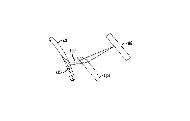
Shown in Fig. 4 is another illustrative embodiment of the invention. In
this arrangement, an optical fiber 401 has a fiber grating 402 thereon which
diffracts the different wavelengths of the optical signal through an optical
element including a glass block 403 and a lens 404 to an optoelectronic chip
406. The optoelectronic chip 406 includes the optical detector and processor
units.
The requirements for monitoring optical signals in WDM
telecommunications are different from most scientific applications in that (1
) we
know the number and approximate wavelengths of the signals, and (2) in
addition to the spectra, our spectrometer can measure fast time-dependent
signals such as bit error rates. We may also need to evaluate the time-
CA 02262764 1999-02-24
g
dependent interactions between spectral elements. Further, it may be highly
desirable for the whole assembly to be compact in size.
Thus, the detector array is designed to measure optical signal intensity
as a function of time and requires high-speed connections to the processing
circuitry. With reference to Fig. 5, to accomplish this high-speed connection
511 the detector array 501 are made integral with the processing circuit 510.
The combining of the detecting and processing functions on the same
optoelectronic chip is, illustratively, accomplished flip-chip bonding type
III-IV
detectors onto a silicon CMOS chip. This fabrication process has been
developed at Bell Labs for high-speed optoelectronic switching using 850 nm
light [e.g., see K. Goossen et al) "GaAs MQW modulators integrated with
silicon CMOS," IEEE Photonics Technology Letters 7, 360-62, 1995].
Extension of the process to 1550 nm light is a relatively straightforward
development involving changing the detector composition to one sensitive to
1550 nm light.
Special high-speed processor circuits can process the detector outputs
before the data is sent off chip. For example an extinction ratio is made by
measuring the average high and low signal values on each detector. A signal-
to-noise ratio (SNR) can be inferred from this measurement, or can be
independently derived by measuring the noise on the channels. This SNR
measurement yields information to evaluate signal transmission quality. The
apriori knowledge about the signals can also be exploited. We know the signal
(if any) must lie within a limited band, so it is possible to cluster the
detectors
into groups (in Figure 2, groups of 5) and use a winner-take-all circuit to
calculate the center wavelengths with simple local processing circuitry.
Further, if changes in wavelength are of particular interest, these can be
calculated for each channel cluster with a hardware derivative circuit
The detector arrays can be implemented using Galium Arsenide (GaAs)
CA 02262764 1999-02-24
9
detectors. Optoelectronic VLSI technologies are available for attaching large
numbers (thousands) of detectors to Silicon VLSI. The detector array may also
be bonded to the integrated circuit processor chip using any of the well known
bonding techniques such as flip-chip, epitaxial lift-off, and heteroepitaxial
growth. The processing ASIC device may process the detected signals by
performing one or functions from a group of functions including at least
filtering,
data reduction, wavelength identification, wavelength power detection, power
discrimination, wavelength shift as a function of time, variation in peak
power
between channels, etc.
With reference to Fig. 5, there is shown a block diagram of an illustrative
opt-electronic chip for detecting and processing of the detected signals. Each
of the optical channel detector units 501 and 502 have multiple detectors (5
per
channel in our example of Fig. 2b) for detecting optical signal intensity
levels
within each of the channels of the WDM signal. The processor 510 includes
separate channel processors 503 and 504, associated with each of the
wavelength optical channel detector units 501 and 502, respectively, for
calculating wavelength center frequency, power levels etc. A higher level
processor unit 505 is used to perform inter-channel comparisons and channel
interaction calculations which require measurements from more than one
channel. Such calculations might include the separation between spectral
peaks, the average and/or peak power variation between channels.
The optoelectonic chip of Fig. 5 takes advantage of the nominal
wavelength separation of the WDM signals and the known number of channels
to integrate monitoring (i.e., detection) capability on the chip. As
previously
discussed since the detector units 501 and 502 are made integral with the
processor 510 the interconnections 511 therebetween is a very high speed
communication connection. The resulting high speed (or high bandwidth)
connection enables real-time high speed signal processing of the detected
CA 02262764 1999-02-24
1~
WDM signals. The detection and processing techniques of the present
invention thus enables the implementation of a smart spectrometer. This is
enabled particularly by the ability to combine large amounts of processing
electronics with the optical signal detectors and arises from the ability to
combine or integrate the detectors directly on the chip with the processing
circuitry. This smart spectrometer can then look at the signals from a number
of detectors over which the desired communication channel is known to appear
and determine whether the signal is at the center of the band, or displaced to
shorter or longer wavelengths. This can be determined by finding the peak
signal channel and by determining the separation from the desired center
channel detector (determined from a previous calibration procedure). This
information can be passed to other parts of the communication system, or used
for real-time active control of the input signal. In addition, if the location
of the
adjacent signal is known, one can monitor the channel separation. Thus the
processors) arrangement may perform functions including filtering, data
reduction, wavelength identification, wavelength power detection, power
discrimination. This processing arrangement also enables the measurement of
fast time-dependent behaviors of the signal, such as the detection of data
modulation and bit error rates.
Since the interconnection between the detector and processor elements
is small, compact, and of high bandwidth, it should be apparent that multiple
separate processing circuits could be present on the same chip, sharing the
connection to the detector(s), should this prove to desirable. An example
might
be the use of two distinct circuits, one for high speed data detection, and
the
other for high sensitivity SNR determination.
What has been described is merely illustrative of the application of
the principles of the present invention. Other arrangements and methods can
be implemented by those skilled in the art without departing from the spirit
and
11
scope of the present invention.