Note: Descriptions are shown in the official language in which they were submitted.
CA 02263339 1999-02-10
- 1
DESCRIPTION
SINGLE CRYSTAL SIC AND A METHOD OF PRODUCING THE SAME
Technical Field
The present invention relates to single crystal SiC and
a method of producing the same, and more particularly to sin-
gle crystal SiC which is used as a substrate Wafer for a high
temperature semiconductor electronic element such as a light-
emitting diode, an X-ray optical element, a switching element,
an amplifying element, and an optical sensor, and also to a
method of producing the same.
Background Art
SiC (silicon carbide) is superior in heat resistance and
mechanical strength than existing semiconductor materials such
as Si (silicon) and GaAs (gallium arsenide), and has good
resistance to radiation. In addition, it is easy to perform
the valence control of electrons and holes by doping an impu-
rity. Moreover, SiC has a wide band gap (for example, single
crystal 6H-SiC has a band gap of about 3.0 eV, and single
crystal 4H-SiC has a band gap of 3.26 eV). Therefore, it is
possible to realize a large capacity, a high-frequency prop-
erty, a dielectric property, and a resistance to environments
which cannot be realized by existing semiconductor materials.
CA 02263339 1999-02-10
- 2 -
SiC receives attention and is expected as a semiconductor
material for a next-generation power device.
As a method of producing (growing) single crystal SiC of
this type, known are a method in which single crystal SiC is
grown by the sublimation and recrystallization method using
a seed crystal, and that in which, in the case of a high tem-
perature, epitaxial growth is conducted on a silicon substrate
by using the chemical vapor deposition method (CVD method),
thereby growing single crystal cubic SiC ((3-SiC).
In the above-described conventional production methods,
however, the crystal growth rate is as low as 1 ~,un/hr. Fur-
thermore, the sublimation and recrystallization method has a
problem in that pin holes which have a diameter of several
microns and which pass through the crystal in the growing
direction remain at about 100 to 1,000/cm2 in a growing crys-
tal. Such pin holes are called micropipe defects and cause a
leakage current when a semiconductor device is fabricated.
These problems block a practical use of single crystal SiC
which has superior characteristics as compared with other
existing semiconductor materials such as Si and GaAs as de-
scribed above.
In the case of the high-temperature CVD method, the sub-
strate temperature is as high as 1,700 to 1,900°C, and it is
required to produce a high-purity reducing atmosphere. There-
fore, the method has a problem in that it is difficult to
CA 02263339 2002-O1-25
-3-
conduct the method from the view point of installation.
Furthermore, the method has another problem in that,
because of epitaxial growth, the growth rate is naturally
limited.
Disclosure of Invention
The invention has been conducted in view of the
above-mentioned circumstances of the prior art. Certain
specific embodiments of the invention may provide large
single crystal SiC of high quality which has a very
reduced number of micropipe defects and the like, and a
method of producing single crystal SiC which can produce
such large single crystal SiC of high quality easily and
efficiently in the view points of installation and
workability, and which can expedite the practical use of
the single crystal as a semiconductor material.
The single crystal SiC of a first aspect of the
invention is characterized in that a complex in which a
single crystal SiC base material and a polycrystalline
plate consisting of Si and C atoms are stacked together
via a smoothed face is subjected to a heat treatment,
whereby polycrystals of the polycrystalline plate are
transformed into a single crystal.
According to this configuration, polycrystals of the
polycrystalline plate may be phase-transformed by only
applying means which thermally processes a complex
consisting of a single crystal SiC base material and a
polycrystalline plate that are stacked together, and
which is simple in the view points of installation and
workability, so that a single crystal is efficiently
grown. Since the single crystal SiC base material and
CA 02263339 2002-O1-25
-4-
the polycrystalline plate are heat-treated via the smooth
face, moreover, no impurity enters the interface between
them from the outside during the heat treatment.
Consequently, it is possible to obtain single crystal SiC
of very high quality which is free from lattice defects
and micropipe defects and also defects such as generation
of grain boundaries due to intrusion of impurities. As a
result, it is possible to attain the effect of expediting
the practical use of single crystal SiC which is superior
in high-temperature property, high-frequency property,
dielectric property, and resistance to environments to
existing semiconductor materials such as Si (silicon) and
GaAs (gallium arsenide), and which is expected as a
semiconductor material for a power device.
The single crystal SiC of a further aspect of the
invention is characterized in that a complex in which a
plurality of single crystal SiC base materials that are
regularly arranged with contacting adjacent side faces to
one another, and a polycrystalline plate consisting of Si
and C atoms are stacked together is subjected to a heat
treatment, whereby polycrystals of the polycrystalline
plate are transformed into a single crystal.
According to this configuration, as a result of the
heat treatment of the complex, it is possible to obtain
single crystal SiC of high quality in which lattice
defects, micropipe defects, generation of grain
boundaries, and the like are little generated.
Furthermore, embodiments of this aspect of the invention
may attain the effects that the side faces of the
plurality of single crystal SiC base materials are
fusedly integrated with each other so that single crystal
SiC which is large in the term of area can be easily
CA 02263339 2002-O1-25
-5-
obtained, and that single crystal SiC which has various
performances superior to existing semiconductor materials
can be applied in variety as a semiconductor material in
the range from a small product to a large product.
In a method of producing single crystal SiC of a
further aspect of the invention, preferably, a single
crystal SiC base material and a polycrystalline plate
consisting of Si and C atoms are smoothed in at least one
face, and the single crystal SiC base material and the
polycrystalline plate are stacked together via the
smoothed face, and the complex is then subjected to a
heat treatment to transform polycrystals of the
polycrystalline plate into a single crystal and grow the
single crystal.
Embodiments of this production method may attain the
effect that single crystal SiC of high quality which has
a very reduced number of lattice defects, micropipe
defects, and grain boundaries is grown easily and
efficiently so that single crystal SiC which is available
as a semiconductor material having a very high
performance can be stably produced and supplied on an
industrial scale.
In a method of producing single crystal SiC of a
further aspect of the invention, a plurality of single
crystal SiC base materials that are regularly arranged
with contacting adjacent sides faces to one another, and
a polycrystalline plate consisting of Si and C atoms are
stacked together, and the complex is then subjected to a
heat treatment, to transform polycrystals of the
polycrystalline plate into a single crystal and grow the
single crystal.
CA 02263339 2002-O1-25
-6-
Using embodiments of this production method, single
crystal SiC of high quality which has a very reduced
number of above-mentioned lattice defects, micropipe
defects, grain boundaries, and the like, and which is
large in the term of area may be efficiently grown,
thereby attaining an effect that single crystal SiC which
is very excellent in performance and which has a wide
application range as a semiconductor material can be
stably produced and supplied on an industrial scale.
In the production methods, when the polycrystalline
plate constituting the complex is an amorphous plate or a
polycrystalline ~i-SiC plate grown on the surfaces of the
plurality of single crystal SiC base materials by the
thermochemical vapor deposition and the thermochemical
vapor deposition temperature of the amorphous plate or
the polycrystalline ~i-SiC plate is set to be in the range
of 1,300 to 1,900°C, such embodiments of the invention
attain an effect that single crystal SiC of high purity
and high quality and having lattice defects and micropipe
defects which are further smaller in number than those of
the single crystal SiC base materials can be obtained
while entering of impurities between the plurality of
single crystal SiC base materials and the polycrystalline
plate on the surface thereof, and diffusion of the
impurities are suppressed.
In the production method, when single crystal SiC
obtained by a heat treatment of a complex is used as the
plurality of single crystal SiC base materials that are
regularly arranged with contacting adjacent side faces to
one another, single crystal SiC which is obtained as a
result of one heat treatment and large in the term of
area may be reused and a heat treatment may be repeatedly
CA 02263339 2002-O1-25
performed, whereby large single crystal SiC which is very
large in area and thickness can be easily produced as a
final product. Therefore, such embodiments of the
invention attain an effect that the application range as
a semiconductor material of high quality can be further
expanded.
Brief Description of Drawings
Fig. 1 is a diagram showing a state of a first
embodiment of the invention before single crystal SiC is
heat-treated, Fig. 2 is a diagram showing' a state of the
first embodiment of the invention after the single
crystal SiC is heat-treated, Fig. 3 is a plan view
showing a state before single crystal SiC of a second
embodiment of the invention is heat-treated, Fig. 4 is a
diagram showing a state of a third embodiment of the
invention before single crystal SiC is heat-treated, Fig.
5 is a schematic bottom view of Fig. 4, Fig. 6 is an
enlarged
CA 02263339 1999-02-10
view of a main portion before the single crystal SiC of the
third embodiment of the invention is heat-treated, Fig. 7 is
an enlarged view of a main portion after the single crystal
SiC of the third embodiment of the invention is heat-treated,
and Fig 8 is a diagram showing a state before single crystal
SiC of a fourth embodiment of the invention is heat-treated.
Best Mode for Carrying Out the Invention
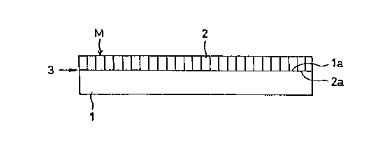
Hereinafter, a first embodiment will be described. Fig.
1 diagrammatically shows a complex M before single crystal SiC
is heat-treated. In the figure, 1 denotes a single crystal
hexagonal a-SiC base material (6H type or 4H type) having a
plate-like shape. The single crystal a-SiC base material 1 is
produced by the sublimation or the Atchison method. The sur-
face la of the base material is smoothly polished. The refer-
ence numeral 2 denotes a polycrystalline cubic ~3-SiC plate
which is separately produced by the thermochemical vapor depo-
sition method (hereinafter, referred to as the thermal CVD
method) in the range of 1,300 to 1,900°C. One face 2a of the
plate is smoothly polished. The polycrystalline (3-SiC plate
2 and the single crystal a-SiC base material 1 are closely
stacked via the polished surfaces 2a and la, thereby producing
a complex M in which crystal faces of different crystal forms
are contacted to each other so as to show a clear linear in-
terface 3.
CA 02263339 1999-02-10
_ g _
Thereafter, the whole of the complex M is subjected to
a heat treatment in which the complex is held for about 8
hours in an atmosphere of a temperature range of 1,850°C or
higher, preferably 2,200 to 2,400°C and a saturated SiC vapor
pressure. As a result, the polycrystalline (3-SiC plate 2 is
transformed into a single crystal, and, as shown in Fig. 2,
polycrystals of the polycrystalline ~i-SiC plate 2 are con-
verted into a single crystal portion 2' which is oriented in
the same direction as the crystal axis of the single crystal
a-SiC base material 1. The single crystal portion 2' is inte-
grated with the single crystal of the single crystal a-SiC
base material 1 to be grown as a large single crystal. After
the heat treatment, the interface 3 which has clearly appeared
before the heat treatment is fusedly integrated to disappear.
As described above, the complex M consisting of the sin-
gle crystal a-SiC base material 1 and the polycrystalline ~i-
SiC plate 2 which are closely contacted to each other via the
smoothly polished faces la and 2a is subjected to a heat
treatment. Therefore, crystal growth mainly consisting of
solid-phase growth, such as that lattice vibration occurs in
the interface 3 to change the atom arrangement is generated.
As a result, single crystal SiC of high quality which has no
micropipe defects and which is substantially free from other
defects such as lattice defects (10 or less per 1 cm2) can be
produced at high productivity. When the single crystal a-SiC
CA 02263339 1999-02-10
- 10 -
base material 1 which has been used in the phase transforma-
tion to an a-single crystal in the polycrystalline ~i-SiC
plate 2 is polished or cut away, it is possible to obtain a
high quality wafer for an electronic device.
Next, a second embodiment will be described. As shown in
Fig. 3, plural single crystal a-SiC base materials 1 ... the
surface of each of which is smoothly polished are regularly
arranged so that the side faces 1b, 1b ... of adjacent single
crystal a-SiC base materials 1 ... are closely contacted to
each other. The polycrystalline /3-SiC plate 2 is stacked on
the polished faces of the plural single crystal a.-SiC base
materials 1 ... which are regularly arranged, in such a manner
that the polished face of the plate is closely contacted to
polished faces. In the same manner as described above, the
complex is then subjected to a heat treatment in which the
complex is held for about 8 hours in an atmosphere of a tem-
perature range of 1,850°C or higher, preferably 2,200 to
2,400°C and in a saturated SiC vapor pressure. As a result,
the polycrystalline (3-SiC plate 2 is transformed into a single
crystal, and a single crystal which is oriented in the same
direction as the crystal axes of the plural single crystal a.-
SiC base materials 1 ... is integrally grown, and the closely
contacted side faces 1b of the adjacent single crystal a-SiC
base materials 1, 1 ... are fusedly integrated with each
other. By repeating this process, single crystal SiC of a
CA 02263339 1999-02-10
- 11 -
large area is obtained.
Next, a third embodiment will be described. Fig. 4 is a
diagram showing a state before single crystal SiC is heat-
treated, and Fig. 5 is a schematic bottom view of the crystal.
Plural single crystal hexagonal a-SiC base materials (6H type
or 4H type) 1 ... are regularly arranged so that the adjacent
side faces 1b, 1b ... are closely contacted to each other. A
polycrystalline cubic (3-SiC plate 2 is grown in a layer-like
manner on the surface of the whole of the plural single crys-
tal oc-SiC base materials 1 by the thermal CVD method in the
range of 1,300 to 1,900°C. In the growing stage of the poly-
crystalline ~i-SiC plate 2, as clearly shown in a microphoto-
graph of an etched section of Fig. 6, a polycrystal member 4
configured by plural single crystal columnar ~i-SiC which are
closely regularly arranged is grown on the surface of the
single crystal a-SiC base materials 1 ... containing lattice
defects, thereby forming a complex M in which the polycrystal
member is contacted to the single crystal oc-SiC base materi-
als 1 at crystal faces of different crystal forms, and which
has an interface 3.
Thereafter, the whole of the complex M is subjected to
a heat treatment in a temperature range of 1,900 to 2,400°C,
preferably 2,000 to 2,200°C and in a saturated SiC vapor pres-
sure. As a result, adjacent ones of the plural single crystal
a-SiC base materials 1 are fused and integrated at the
CA 02263339 1999-02-10
- 12 -
closely contacted side faces 1b, 1b, and the polycrystal mem-
ber 4 of the polycrystalline (3-SiC plate 2 is transformed into
single crystal a.-SiC, so that a large single crystal 5 which
is oriented in the same direction as the crystal axes of the
single crystal oc-SiC base materials 1 ... and integrated with
the single crystals of the base materials 1 is grown.
As described above, the complex M in which the polycrys-
tal member 4 of the polycrystalline ~i-SiC plate 2 is grown by
the thermal CVD method on the surfaces of the plural single
crystal a-SiC base materials 1 that are regularly arranged so
that the adjacent side faces are closely contacted to each
other is subjected to a heat treatment. Therefore, crystal
growth which is very large in the term of area and which
mainly consists of solid-phase growth, such as that lattice
vibration occurs in the interface 3 to change the atom ar-
rangement is generated. As a result, as clearly shown in a
microphotograph of an etched section of Fig. 7, single crystal
SiC 1' of high quality which is substantially free from lat
tice defects and micropipe defects (10 or less per 1 cmz) can
be easily produced.
Next, a fourth embodiment will be described. In the
fourth embodiment, plural high quality single crystal SiC 1'
which are produced in the manner described in the third em-
bodiment are reused as single crystal ot-SiC base material.
Specifically, as shown in Fig. 8, the plural high quality
CA 02263339 1999-02-10
- 13 -
single crystal SiC 1' .., are regularly arranged so that adja-
cent side faces 1'b, 1'b are closely contacted to each other.
The polycrystalline plate 2 having the orientation configured
by plural single crystal cubic (3-SiC which are closely ar-
ranged is grown by the thermal CVD method on the surface of
the whole of the plural single crystal SiC 1' . . . , thereby
forming a complex M'. Thereafter, the whole of the complex M'
is subjected to a heat treatment in a temperature range of
1,900 to 2,400°C, preferably 2,000 to 2,200°C and in a satu-
rated SiC vapor pressure in the same manner as Embodiment 3
described above. As a result, a high quality single crystal
SiC of a desired size can be easily produced as a final prod-
uct.
In the embodiments, the single crystal a-SiC base mate-
rial 1 is used as the single crystal SiC base material. Alter-
natively, for example, an a-SiC sintered member or a single
crystal ~i-SiC member may be used. In the embodiments, the
polycrystalline (3-SiC plate 2 is used as the polycrystalline
plate consisting of Si and C atoms. Alternatively, for exam-
ple, a polycrystalline a-SiC plate, an SiC sintered member of
high purity, or an amorphous plate of high purity (1O14a~~~3~
or less may be used, and it is possible to obtain single crys-
tal SiC of high quality in the same manner as the embodiments.
As the single crystal a-SiC base material 1 in the em-
bodiments, either of the 6H type or the 4H type may be used.
CA 02263339 1999-02-10
- 14 -
When the 6H type is used, a single crystal which is converted
from polycrystals of the polycrystalline ~i-SiC plate 2 into
a-SiC as the progress of the heat treatment is easily grown
in the same form as that of a single crystal of the 6H type.
When the single crystal base material 1 of the 4H type is
used, a single crystal in the same form as that of a single
crystal of the 4H type is easily converted and grown as the
progress of the heat treatment.
Preferably, the temperature conditions of the heat treat-
ment of the complex M are set to be in the range of 1,850 to
2,400°C, preferably, 2,000 to 2,200°C. When the temperature of
the heat treatment is lower than 1,850°C, the kinetic energy
of atoms cannot be given to many SiC constituting the inter-
face. When the temperature is higher than 2,400°C, thermal
energy which is very higher than the decomposition energy of
SiC is supplied and crystals of SiC themselves are decomposed.
Industrial Applicability
As described above, the invention is a technique that a
complex in which a single crystal SiC base material and a
polycrystalline plate are closely stacked together via a
smooth polished face or a polycrystalline plate is grown by
the thermal CVD method on the surfaces of plural single crys-
tal SiC base materials that are regularly arranged with con-
tacting the side faces to one another is subjected to a heat
CA 02263339 1999-02-10
- 15 -
treatment, so that polycrystals of the polycrystalline plate
are transformed into a single crystal, and a single crystal
oriented in the same direction as the crystal axis of the
single crystal SiC base material is integrally grown to a
large size, whereby a large single crystal of high quality
which is superior in heat resistance and mechanical strength
and which has a very reduced number of micropipe defects and
lattice defects can be produced easily and efficiently.