Note: Descriptions are shown in the official language in which they were submitted.
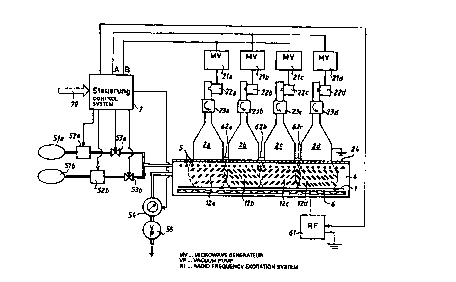
?CA 02264017 l999-02- 19SPECIFICATIONPLASMA CVD SYSTEM WITH AN ARRAY OF MICROWAVE PLASMA ELECTRODESAND PLASMA CVD PROCESSThe invention relates to a plasrna-supported equipment for chemicalgas phase deposition with an array type arrangement of microwave plasmaelectrodes and a control circuit, and also to a corresponding coatingprocess.The like is known from US 5,017,404 (DE 38 30 249 C2). It is thereprovided that the individual plasma electrodes are arranged such that theplasma columns which are produced, overlap. The individual plasmaelectrodes are switchable and controllable independently of each other bymeans of the supplied electronic power, and in fact this is used to equalizeedge effects or to produce a specific course of the coating properties. It isexpressly a prerequisite that disturbing interference effects do not occurwith the high frequency fields.The application to the field of plasma pulse CV D technology isdescribed, as are examples of microwave antennas and the like. Theexamples relate to two-dimensional arrays.The said US 5,017,404 is expressly incorporated by reference into thedisclosure of this Application. The embodiment of apparatus systems areto be gathered therefrom and are suitable for the suitable control of theplasma electrodes for the embodiment of the invention.In the case of high requirements on the homogeneity of large-surfacelayers it has been found that interference of adjacent microwave ?elds still?CA 02264017 l999-02- 19-2-disadvantageously appears, in contrast to the said document, when there isoptimum shaping of the overlap of the plasma columns.(European Patent) EP 0 420 117 A describes the disturbance due tointerference in plasma CV D with excitation by a microwave array, andconsiders a stable operation to be impossible without their elimination. Itis proposed to provide different polarizations, i.e., directions of the electric?eld vector, in adjacent microwave sources.However, attaining homogeneous excitation behavior in theindividual modules is obviously made more difficult here, since thecrossed rectangular waveguides which are shown in the examples do notpermit (this) because of the asymmetrical waveguide geometry.Another kind of interference prevention would be the frequencydisplacement of adjacent plasma electrodes. Commercial microwavegenerators have marked frequency ?uctuations and also high bandwidths,especially in pulsed operation, so that relatively large frequency differenceswould be required. However, different plasma-chemical modes ofbehavior can then no longer be excluded. In addition, microwavegenerators of optional frequency are not immediately available, sinceeconomical operation is only possible for permitted industrial frequencies.The usual plasma CV D processes are characterized in that thereaction gas ?ows over the substrate during the whole coating period, andsimultaneously energy which produces plasma is introduced into thereaction volume, so that the reaction gas and exhaust gas of an alreadysuccessful (film-forming, etc.) reaction are either mixed in a manner whichis not clearly arranged, or occur in different proportions at differentlocations of the substrate. The speed of a development, the properties of?CA 02264017 l999-02- 19-3-the coating (especially density, adhesion strength, and stability), and alsothe yield of reaction gas, are limited.Such limitations are overcome by the application of the plasma pulseCV D process (PICV D process).In this process, the energy which generates plasma is introduced inpulsed form, while the reaction gas ?ows continuously into the reactionspace. It is typical for the PICV D process that the interval between pulsesis matched to the time required to completely replace with fresh gas the gasVolume over the substrate and implicated in the (film-forming) reaction.This time is dependent on several parameters, such as, for example,substrate size and shape, mass ?ow and temperature of the reaction gas,pressure in the reactor, and kind of gas in?ow (e.g., nozzle form).The process operates like a twoâstroke motor; the interval betweenpulses, in which the used gas is replaced by fresh gas, follows the fllII1-forming plasma pulse.A further advantage of this process is the low temperature loading ofthe substrate, since the action of energy on it takes place only during thepulse period, and the substrate cools in the interval between pulses. It isthereby possible, vice versa, to use comparatively high energies during thepulse, and thus to deposit films with properties which otherwise only thesolid material has.The values for the pulse duration are typically between 0.1 and 10ms, and for the duration of the interval between pulses, between 10 and100 ms.It is favorable to irradiate with microwave energy, since plasmas arethen produced at gas pressures in the mbar region. Such gas pressures can?CA 02264017 l999-02- 19-4-be produced with comparatively little expense. The PICVD process can beadvantageously applied, for example, for the internal coating of dielectrictubes from which, for example, preforms for optical ?bers are produced(EP 0 036 191, DE 38 30 622, DE 40 34 211), for the application of IR-transparent dielectric mirrors to glass substrates of spherical surface shape(DE 40 O8 405, DE 43 34 572), or for the deposition of planar thin filmwaveguides on glass or plastic (DE 41 37 606, DE 42 28 853).The present invention has as its object the preparation of a plasmaCV D equipment of the kind under consideration, and a correspondingprocess, wherein optional scalability of the dimensions of the coating unitand outstanding homogeneity of the films produced, with economicconstruction, are attained.The object is attained with an equipment according to claim 1 andcorrespondingly with a process according to claim 7.The decoupling with respect to time of the microwave excitation ofadjacent plasma electrodes is seen as a further possibility of the preventionof interference. The microwave power can be cycled substantially fasterthan corresponds to the pulse duration of a plasma pulse CV D process(PICV D) pulse which exhausts the gas supply. Adjacent plasma electrodescan thereby be cycled at staggered times, without resulting in a disturbingeffect on the plasma and on the deposition behavior of the PICVD process.According to claim 2 or 8, the pulse duration is at most 50microseconds, and is thus markedly shorter than the typical time constantsof the gas chemistry concerned, of about 100 microseconds.According to the invention, the simultaneously coated surfaces canbe optionally scaled, with a modular system. The knowledge gained with a?CA 02264017 l999-02- 19-5-few modules can be applied to an array with optionally many modules.Further advantageous embodiments are the subject of the dependentclaims 3-6 or 9-13, respectively.According to claim 3 or 9, a few tens of pulses to a few hundredpulses, respectively offset in time for adjacent plasma electrodes, can forma total pulse of the PICV D process.Claims 4 and 10 give the combination with a radiofrequency (RF)excitation. In connection with the microwave excitation according to theinvention, this permits a further increase in uniformity of the films, bysuitable control of the field distribution by means of a suitabledimensioning of the spacing and extent of the RF electrodes. The RFexcitation can also be pulsed, either synchronously with the microwaves(indeed, for energy saving) or else in another appropriate time sequence.The combination of microwave and radiofrequency excitation isknown page from Moisan M., Wertheimer M.R., Surface and CoatingsTechnology §_9_ (1993), pp. 1-13. The object in that case was the alteration ofthe film quality by ion bombardment. Here, in contrast, the ease withwhich the ?eld lines of the RF excitation can be shaped is used in order toimprove the homogeneity of the film.Uniformity can also be increased by the use of magnetic ?elds toaffect the transition region between two plasma electrodes, and also by asuitably structured gas supply.In particular with a linear array, as is provided according to claims 5-11, according to claims 6 and 12 only two different phase-displaced cyclesare required for the interference-free pulsing of all the plasma electrodes,thus effectively limiting the cost of control and of microwave production.?CA 022640l7 l999-02- 19-6-The invention will be described in more detail with reference to theaccompanying drawings.Fig. 1 schematically shows a plasma CV D equipment;Fig. 2 schematically shows the time course of the microwave excita-tion;Fig. 3 schematically shows a foil coating equipment.The plasma CV D equipment shown in Fig. 1 contains a substrate 1,e.g., a glass plate. Numerous microwave antennas, here four, 2a-2d, arearranged in a row, or else in a ?at array, opposite the substrate 1. Thesehorn microwave antennas 2a-2d act as microwave plasma electrodes andare supplied by microwave generators 21a-21d by means of magnetrons22a-22d and isolators 23a-23d. A microwave window 24, e.g., just like thesubstrate 1 and also itself ready for coating, closes the vacuum chamber 4with respect to the microwave antennas 2a-2d. The substrate is arrangedopposite and parallel in the vacuum chamber 4.The process gas is supplied from gas containers 51a, 51b via massflow regulators 52a, 52b, gas valves 53a, 53b, and the uniformly distributedgas inlets 5 to the vacuum chamber 4, and the used residual gas is suckedout again via a pressure regulator 54 by a Vacuum pump 55.A control 7 suitably sets all these parts corresponding topredetermined parameters, via an interface 70.So far, the equipment corresponds to the known plasma CV D equip-?CA 02264017 l999-02- 19-7-ments, in particular also PICVD equipments and US 5,017,404 (DE 38 30249 C2).The special feature is that the microwave generators 21a-21d areseparately driven by the control 7 in two groups 21a, 21c and 21b, 21d withsignals A or B, and indeed with pulse trains of short micropulses 20A or20B, which have a pushâpull phase displacement. Thus only one ofadjacent microwave antennas 2a, 2b; 2b, 2c; 2c, 2d is active at a time, so thatinterference is excluded. Fig. 2 shows the course of these pulses. The pulseduration and interval of the micropulses A and B together form a pulse ofabout 0.5 ms duration according to the PICV D process.The measures of US 5,017,404 can be combined with the invention forthe speci?c setting of the course of film thickness by means of the antennaarray.The resulting plasma zones 12a-12d overlap in their edge regionswith decreasing deposition power without interference effects, so that astable, uniform transition is effected by matching the antenna geometry atthe transition regions 62a-62d. The matching of the regions 62a-62dlikewise serves for the optimum formation of the RF ?eld.The number of microwave antennas 2a-2d in a row is a randomlychosen example. The modules, typically covering a few centimeters, ofmicrowave generator 21i, magnetron 22i, isolator 23i and horn antenna 2i (iis from 1 to n), can be arrayed in optional number, e.g., to two or threemeters of width for the coating of large ?at glass sheets or of lengths of foil.The following process examples illustrate the process:Process Example 1:?CA 02264017 l999-02- 19-3-The vacuum chamber 4 is first pumped out to well below the desiredprocess pressure. A gas mixture suitable for coating is thereafter producedby means of the mass ?ow regulators 52a, 52b and also the valves 53a, 53b.For the deposition of SiO2, this mixture can, e.g., consist of 200 sccm(standard cubic centimeters) of oxygen and also 20 sccm of hexamethyldisiloxane (HMDSO). During the whole coating process, these gases flowcontinuously (not pulsedl). A process pressure of 1 mbar is set by means ofthe pressure regulator unit 54. As soon as this has been reached, themicrowave generators 21 a, 21d are driven with the pulse sequence given inFig. 2.Each pulse train A, B consists, according to Fig. 2, of 10 individualpulses ("micropulses") of 25 its duration each and phase displaced in push-pull at the outlet A and B. During the micropulses, the total of whichrepresents a typical PICV D "macro pulse", the coating gas mixture in theplasma space 12a-12d is converted, and diffuses to the substrate 1, onwhich the desired SiO2 layer is deposited.After the end of a "macro pulse", the reacted gas mixture is suckedout and is replaced by fresh gas mixture. For a complete gas exchange, theinterval between two macro pulses is typically 10-100 ms long (dependingon the geometry of the vacuum chamber 4). After the interval betweenpulses, the micropulse sequence of a macro pulse is again driven, in orderto deposit the next film layer, until the reference thickness has beenreached. The vacuum chamber 4 is thereafter brought to normal pressure,and the coated substrate 1 can be removed.Process Example 2:?CA 02264017 l999-02- 19-9-The process and its parameters run similarly to those in Example 1,but the substrate this time is a ?exible foil 301 which is continuouslymoved in the coating chamber 304. Fig. 3 shows a cross section of thearrangement with a winding device 341, 342 for the foil 301.The speed of the foil is adjusted so that each surface element of thefoil is coated with the speci?ed film thickness. With typical depositionrates of 500 nm per minute and a specified thickness of 50 nm, the coil 301must pass through the plasma region 305 in six seconds. It is thereby alsoinsured that the movement of the foil 301 during a rnicro-pulse isnegligible.Process Example 3The process proceeds as in Example 2, but during a macro pulse, andalso a millisecond before and after it, an RF field is turned on. Thegeometrical structure of the RF electrode 306, with a reduced electrodespacing in the region of the interface of two microwave antennas 302a,302b, enables the non-uniforrnities at the interfaces to be compensated.The power of the RF generator can thus be set to optimum film uniformity.In a through?ow equipment, the RF power is subject to feedback controlby means of thickness measurement after the coating.