Note: Descriptions are shown in the official language in which they were submitted.
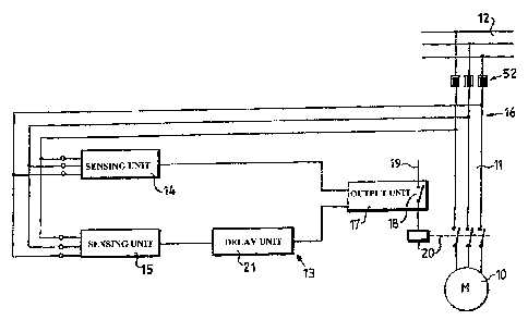
?1015202530CA 02264056 l999-02- 19Phase monitorThe present invention relates to a phase monitorfor a shortâcircuited asynchronous threeâphase motor.More particularly, the invention relates to sucha phase monitor of the kind comprising sensing means,intended to be connected to a supply voltage line tothe motor in order to sense the voltage conditions onsaid line, a control switch, controlled by said sensingmeans and intended to be connected in a control circuitfor a supply voltage switch for the motor in order toclose and open said control circuit in dependence uponthe sensed voltage conditions on said line, said supplyvoltage switch being connected in the supply voltageline at a location between the connection point of saidsensing means and the motor, and delay means for delayingthe switchingâon and switchingâoff operations of thecontrol switch.Such phase monitors are commonly utilized to preventdamages and injuries caused by phaseâsequence faults orphase voltage dropâouts in the supply voltage to themotor. Normally, phaseâsequence faults do not occur inpermanent installations,since, in the case of such in-stallations, once the motor has been installed and con-nected in a correct manner to a power distribution network,the phase sequence till normally not be altered. However,in the case of portable equipments, such as those connectedto the mains via plug contacts, there is a high risk ofphaseâsequence faults. Phase voltage dropâouts, on theother hand, may occur to the same extent at permanent in-stallations as at portable equipments.The delay means contained in the phase monitorhave for their purpose to prevent normal voltage varia-tions on the mains from causing alternating switchingâonand switchingâoff operations of the control switch andhence also of the supply voltage switch for the motor.?101520253035CA 02264056 l999-02- 19However. when using phase monitors of the abovekind previously known, the delay of the switching-onoperation has been found to cause a serious problem.Especially in the case of portable equipments, said delaymay very well result in that, when, as a consequence ofsaid delay, the motor does not start immediately upon aconnection of the supply voltage line to the mains, anoperator may shift the phase sequence of the voltageapplied on the supply voltage line and then leave themotor connected to a supply voltage having an incorrectphase sequence. The invention has for its purpose toprovide an improved phase monitor of the kind initiallyspecified which avoids the risk of such serios mistakesmade by an operator.The phase monitor, according to the invention pro-posed for said purpose, is primarily characterized in thatsaid sensing means comprise, on the one hand, a firstsensing unit which is operatively connected to the controlswitch without the intermediary of any delay means andwhich is arranged to cause an immediate switching-onoperation of the control switch when the supply voltageline is connected to a supply voltage source, if thevoltage conditions on the supply voltage line sensedby said first sensing unit at the connection moment areacceptable, and on the other hand, a sensing unit whichis operatively connected to the control switch through theintermediary of said delay means and which is arranged,upon a preceding switching-on operation of the controlswitch caused by said first sensing unit, to cause adelayed control of the state of the control switch independence upon the voltage conditions on the supplyvoltage line sensed by said second sensing unit.The invention guarantees that, when the supplyvoltage line is connected in a correct manner withrespect to the phase sequence to a mains on which anyphase voltage dropâout does not exist, the motor will?101520253035CA 02264056 l999-02- 19start rotating in the correct direction almost immediate-ly, while, after a switchingâoff operation of the controlswitch caused by a later phase voltage drop-out, it willnot be restarted until correct voltages have againexisted on all three phases during a time correspondingto the switchingâon delay caused by said delay means.. In previously known phase monitors of the abovekind, it has usually been necessary to make the switching-off delay shorter than the switchingâon delay. However,according to the invention, the delay means may preferablybe arranged to cause a substantially longer delay ofa switchingâoff operation of the control switch causedby the second sensing unit than of a repeated switching-on operation of the control switch subsequently causedby thissensing unit. Such a function of the delay meansis especially favourable if the mains to which the voltagesupply line is connected is of inferior quality and highlysensitive to variations in its load.The transfer of the control of the control switchfrom the first sensing unit to the second sensing unitafter a switchingâon operation of the control switchcaused by the first sensing unit may be obtained indifferent ways. In order to facilitate said transferof the control function, the second sensing unit may how-ever suitably have a substantially higher sensitivity toany occurring variations in the amplitude of and the phasedisplacement between the phase voltages on the supplyvoltage line than does the first sensing unit have.Below, the invention will be described in furtherdetail with reference to the accompanying drawings, inwhich:-Figure 1 shows a block diagram of a phase monitoraccording to an embodiment of the invention selectedby way of example, illustrating the phase monitor con-nected to a supply voltage line to an electric three-phase motor,?101520253035CA 02264056 l999-02- 19Figure 2 shows a circuit diagram, illustratingone possible design of one of two sensing units containedin the phase monitor,Figure 3 shows a circuit diagram, illustratingone possible design of a delay unit contained in thephase monitor, andI Figure 4 shows a circuit diagram, illustratingone possible design of an output unit of the phase monitor.In Figure 1, reference numeral 10 designates anelectric motor, consisting of a shortâcircuited asynchro-nous three~phase motor, and reference numeral 11 designa-tes a supply voltage line to the motor through which themotor may be connected to a mains 12 in order to besupplied with the required supply voltage from said mains.Figure 1 also shows a connector 52 serving to connectline 11 to mains 12 and consisting of a threeâpole plug,connected to line 11, and a three-pole socket, connectedto mains 12.In order to prevent a phaseâsequence fault causedby an incorrect connection of line 11 to mains 12 ora voltage dropâout on any of the three phases of mains12 from causing any damages or accidents, there is pro-vided a phase monitor generally designated 13. This phasemonitor comprises a first sensing unit 14 and a secondsensing unit 15 both of which are connected to line 11at a point 16 in order to sense the voltage conditionson line 11 at said point. Furthermore, phase monitor 13also comprises an output unit 17, containing a controlswitch 18 which is connected in a control circuit 19(only partially shown) for a supply voltage switch 20for the motor, connected in supply voltage line 11 ata location between the connection point 16 of the twosensing units and motor 10, and which serves to closeand open control circuit 19 in dependence upon the sensed.voltage conditions on line 11 at point 16. Finally, phasemonitor 13 also comprises a delay unit 21, connected?101520253035CA 02264056 l999-02- 19between the second sensing unit 15 and output unit 17.While sensing unit 15 thus is connected to output unit17 via delay unit 21, sensing unit 14 is instead directlyconnected to output unit 17 without the intermediaryof any delay unit.Sensing unit 14 serves to sense the voltage condi-tions on line 11 at the moment when said line is connectedto mains 12 and to cause an almost immediate switchingâonoperation of control switch 18 and hence also of supplyvoltage switch 20 if the voltage conditions on line 11sensed at the connection moment are acceptable, i.e.if any phaseâsequence fault or any phase voltage dropâoutdoes not exist.Sensing unit 15 instead serves to sense the voltageconditions on line 11 continuously once motor 10 hasbeen connected to said line by a switchingâon operationof the two switches 18 and 20 caused by sensing unit14 and then to control the positions of said two switchesin dependence upon the voltage conditions on line 11.If a phase voltage dropâout occurs when motor 10 is inoperation, sensing unit 15 will cause a switchingâoffoperation of switches 18 and 20 to occur after a pre-determined time, determined by a switchingâoff delaycaused by delay unit 21. Motor 10 will then be stopped.When the phase voltage interruption ceases, sensing unit15 causes a repeated switchingâon operation of switches18 and 20 and a restart of motor 10 after another pre-determined time, determined by a switchingâon delay causedby delay unit 21.In order to provide the functions above described,sensing units 14 and 15, output unit 17 and delay unit 21may for instance be designed in the manner describedbelow with reference to Figures 2, 3 and 4.Figure 2 shows a circuit diagram of a design ofsensing unit 14, selected by way of example. In theillustrated case, unit 14 comprises three phase circuits?101520253035CA 02264056 l999-02- 19which are intended to be connected each to one phaseL1, L2 and L3, respectively, of line 11 and each of whichconsists of a resistor 22, a diode 23, a diode 24, acapacitor 25, a resistor 26, a Schmittâtrigger 27 havingan inverted output, and a diode 28. Moreover, unit 14also comprises a logic detector which is connected todiode 28 of each of the three starâconnected phase cir-cuits and which consists of four resistors 29, 30, 31and 32, two capacitors 33 and 34, two Schmittâtriggercircuits 35 and 36 having inverted outputs, a diode 37and an inverter 38.The aboveâmentioned phase circuits 22 â 28 andthe logic detector 29 â 38 connected thereto operatein the following manner. Capacitor 33 acts as an energystorage capacitor which is continuously charged in apositive direction via resistors 29 and 30 but which,if the three phase circuits are supplied with voltagesfrom line 11 (Figure 1) which are mutually displacedby about 120°, also continuously will receive negativepulses or discharge pulses from the phase circuits atsufficiently short intervals to make sure that the voltageacross the capacitor will be maintained at a low level,corresponding to a logic "0". The output signal fromthe logic detector, i.e. the signal at the output ofinverter 38, will then consist of a logic "1".If as a consequence of a phase voltage drop-outon mains 12, any voltage does not exist on one of thephases of line 11, the corresponding phase circuit ofunit 14 will not deliver any discharge pulse to capacitor33. In this case, the two remaining discharge pulsescannot maintain the voltage across capacitor 33 on alow level, corresponding to a logic "0". Instead, saidvoltage will reach a higher level, corresponding to alogic "1". This means in its turn that the output signalfrom the logic detector will consist of a logic "0" andno longer of a logic "1".?101520253035CA 02264056 l999-02- 19In order to make it possible by means of unit 14to detect not only any phase voltage dropâout existingon mains 12 at the moment of connecting line 11 to themains but also any phaseâsequence fault caused as a con-sequence of an incorrect connection of said line to themains, unit 14 is also provided with a diode 39 whichis connected between two of the phase circuits previouslydescribed. If a phaseâsequence fault exists, said diodewill eliminate the generation of discharge pulses inone of the phase circuits. The logic detector will there-for react on a phaseâsequence fault in the same manneras on a phase voltage dropâout, i.e. the detector willdeliver an output signal corresponding to a logic "0".Sensing unit 15 may be built up in the same manneras sensing unit 14. Since any phaseâsequence fault normallycannot occur once line 11 has been connected in a correctmanner to mains 12, diode 39, shown in Figure 2 and servingto detect such faults, may however be omitted in unit 15.In order to make sure that sensing unit 15 willdetect any phase voltage drop-out occurring during theoperation of motor 10, it is necessary that this unitis highly sensitive to variations in the amplitude ofand the phase displacement between the phase voltagesoccurring on line 11. The reason is that in the eventof any dropâout of the voltage on one of the three phaseconductors of line 11, motor 10 will supply said phaseconductor with an induced voltage, the phase angle ofwhich differs from the phase angle of the normal voltageon said phase conductor only by 10° â 15° and the amplitudeof which may be of the same order as the amplitude ofthe normal voltage on said phase conductor. Sensing unit14 on the other hand may not have a corresponding highsensitivity as said unit is not intended to respond toany phase voltage drop-out occurring when the motor isin operation. Accordingly, unit 14 should have a sub-stantially lower sensitivity to the amplitude and the?101520253035CA 02264056 l999-02- 19phase angle of the phase voltages occurring on line 11than does unit 15 have. This difference in voltage sen-sitivity between units 14 and 15 may be obtained byselecting the time constant for charging capacitor 33differently for said two units.Figure 3 shows a circuit diagram of a design ofdelay unit 21, selected by way of example. As previouslymentioned, the input of said unit is connected to the15. unit21 comprises two delay circuits which are connected inoutput of sensing unit In the illustrated case,series. The first delay circuit is arranged to causea predetermined switchingâon and switchingâoff delayand consists of two resistors 40 and 41, a diode 42 anda capacitor 43. The second delay circuit consists oftwo Schmittâtrigger circuits 44 and 45, a diode 46, aresistor 47 and a capacitor 48 and it is arranged tocause a predetermined additional switchingâoff delaywhich preferably may be substantially longer than theswitchingâon and switchingâoff delay caused by the firstdelay circuit.Figure 4 shows a circuit diagram of output unit 17.This unit consists of an ANDâgate 49, a resistor 50,a transistor 51 and the previously mentioned controlswitch 18, intended to be connected in control circuit19 (Figure 1). One input of ANDâgate 49 is connectedto the output of sensing unit 14, while the other inputof said gate is connected to the output of delay unit 21.12,is connected to the mains in such a manner as to bringIf, when connecting line 11 to mains said linethe different phase voltages to appear in correct phasesequence on line 11 and any phase voltage drop-out doesnot exist on the mains, ANDâgate 49 will receive signalscorresponding to a logic "1" from sensing unit 14 aswell as from delay unit 21 which is such that it willalways initially deliver an output signal corresponding"1"to a logic . Transistor 51 will then cause a switching-?1015202530CA 02264056 l999-02- 19on operation of control switch 18. If a phaseâsequencefault exists, the input signal to ANDâgate 49 from unit14 will instead consist of a logic "0", which means thatany switchingâon operation of control switch 18 willnot take place. In the same manner, any switchingâonoperation of switch 18 will neither occur if a phasevoltage dropâout exists on mains 12 when line 11 isconnected thereto.The reason why delay unit 21 always initially gene-rates an output signal consisting of a logic "1" at thetime of connecting line 11 to mains 12 is that capacitor48 then maintains the input of circuit 45 on a low level.The DC voltage supply to resistor 47 and to all othercomponents connected to a positive DC voltage terminalis namely not started until said time by means of a DCvoltage generating circuit (not shown)one of diodes 24 (Figure 2)., connected toIf a phase voltage dropâout occurs on line 11 whilemotor 10 is in operation, the low sensitivity of sensingunit 14 will result in that the output signal fed toANDâgate 49 from said unit will remain a logic "1". How-ever, after the total switchingâoff delay determinedby the two delay circuits in delay unit 21, the signalfed to ANDâgate 49 from said unit will shift to a logic"0" and cause a switchingâoff operation of control switch18. When, later on, the phase voltage in question returns,the output signal from delay unit 21 will shift backto a logic "1" and cause a renewed switchingâon operationof control switch 18 after a time corresponding to theswitchingâon delay caused by said unit.The invention is not restricted to the embodimentabove described and shown in the drawings. Instead, manyother embodiments are feasible within the scope of theinvention as defined in the following claims.