Note: Descriptions are shown in the official language in which they were submitted.
CA 02264724 1999-03-01
.. . .. . ..
~ 100~ _ i
WO 9~ PCT/DE97/Ol ~S7
[TRANSLATION~
D e s c r i p t i o n
Layer sequence and a component containing same
The invention relates to a layer sequence according to the
preamble of claims 1 and 2. The invention relates, further,
to a cryogenic component according to the preamble of claim 7.
The invention further relates to a layer sequence according to
the preamble of claim 10. The invention further relates to a
cryogenic component according to the preamble of claim 15.
With respect to the invention according to patent claims 1
through 9, the following can be stated:
The basis for components in superconductivity electronics
is an epitactic multilayer system with at least one layer
sequence in which the superconductive material forms boundary
interfaces with nonsuperconductive materials. If the component
is to be grown on a desired substrate a buffer layer can
optionally be required.
The following are known as state of the art:
1. Components of superconductivity electronics
Epitactic layer sequences or multilayer systems for such
components are comprised of one or more thin films of a super-
conductive material and one or more thin films of nonsuper-
--1--
CA 02264724 1999-03-01
21008
WO 9~1/0933J ~'-/uE97lo1~7
conductive material. These nonsuperconductive materials are
effective as barrier materials in Josephson contacts
{junctions}, for passivation or as a diffusion block. Based
on the characteristics of the high-temrerature superconductor,
the following are the requirements for the nonsuperconductors:
The high temperature superconductive and the nonsuper-
conductive materials must be chemically compatible. This meAns
that no chemical reactions should occur between the materials.
The nonsuperconductive material should be able to grow
epitaxially on the high-temperature super-conductive material
and the high-temperature superconductive material should be
correspondingly able to grow on the nonsuperconductive
material with, indeed, the desired crystallographic
orientation. The thus-resulting boundary interfaces should be
atomically sharp and should not contain any defect-oriented
regions or extraneous phases in their environs. Because of
the relatively high fabrication temperatures of the layers, an
interdiffusion of ions cannot be excluded and hence it must be
ensured that any extraneous ions which are in the material
affect the properties thereof to the smallest extent possible.
It is, for example, known that above all small ions like those
of Al, Ga, Ti, W, Fe, and Zn, or even Ce, Pr, reduce the
superconductivity of the high-temperature superconductor
REBa2Cu3o7-z -
CA 02264724 l999-03-Ol
21008
WO 9~ # PCT/DE97/O1~57
This applies inter al ia also to the oxygen content and the
ordering of the oxygen atoms in the high-temperature
superconductors in which the ~uperconductivity i8 weakened by
oxygen loss or oxygen disordering. A high degree of chemical
compatibility is required when the nonsuperconductive material
is used, for example, as thin barriers in Josephson junctions.
Because of the reduced coherency lengths of high-temperature
superconductors - typically in the range of 1 nm to 2 nm - it
is required that the barrier material not have its coherency
length, which is in the length range of the ordering parameter
of the superconductive electrodes in the proximity of the
boundary interface, reduced for example by ion diffusion or
lattice dislocation. Up to now no material has been known
which fulfills this requirement satisfactorily.
Materials research has been concentrated on two material
classes. One class is oriented upon the structure of
REBa2Cu307z. The research here is in targeted replacement and
doping with one or more ion types which reduce the super-
conductive properties or even completely suppress them. The
second class encompasses Perovskite or Perovskite-like
compounds. From each class at an appropriate location, one
material will be discussed.
The nonsuperconductive material PrBazCu307z differs
chemically from YBa2Cu307z only by the substitution of Y by Pr
CA 02264724 1999-03-01
21008
WO 9~/0933~ P~; I /uE97/01~
which effects the loss of superconductivity. The lattice-
defect match with YBa2Cu3O7z ~mounts to only 1%. By comparison
to most of the other, hitherto researched, nonsuperconductive
materials, PrBa2Cu3O72 has the highest degree of chemical and
structural compatibility with YBa2Cu3O7z. For example, a
monolayer of YBa2Cu3O7z, which serves as the intermediate layer
in a PrBa2Cu3O,z matrix, has a critical temperature {Tc} of 30R
(T. Terashima et al, Phys. Rev. Lett . 67, 1362 ( 1991)).
Similar experiments with other nonsuperconductive
materials show that these values cannot be attained with any
other material. Substantial disadvantages of PrBa2Cu3O7z are,
however, its relatively low specific resistance, which ~-kes
it less than satisfactory for insulation purposes, and the
reduction of the ordering parameter at the boundary interface
as a result of diffusion of Pr ions into the YBa2Cu3O7z. If one
replaces for example only 5% of the Y atoms in YBa2Cu3O7z by Pr
atoms, the critical temperature is already reduced from 92K to
85K (M.S. Hedge, et al., Phys. Rev. B 48, 6465 (1993)).
A typical representative of the second class of
Perovskite-like compounds is SrTiO3. This material has a cubic
crystal structure whose lattice-defect matching to YBa2Cu3O7z
amounts to 1.2%. The specific resistance at 200 MQcm is
clearly greater than that for PrBa2Cu3O7z. It shows that with
this material a heteroepitaxy is possible with YBa2Cu3O7z. The
--4--
CA 02264724 1999-03-01
21008
WO 91~1093~ PCT/OE97/Ol#S~
chemical compatibility of the materials is, however, limited.
The diffusion of Ti ions as well as their incorporation in the
Cu sites of YBa2Cu3O7z gives rise to a reduction of the
ordering parameter in the vicinity of the boundary interface.
Furthermore, the lattice distortion in the YBa2Cu3O~z,
resulting from the boundary interface with the SrTiO3, reduces
the ordering parameter in a noticeable manner.
2. Buffer layers
Application-oriented requirements can make it desirable to
grow high-temperature superconductor thin layers or a
component containing such a layer on a substrate which is not
suitable, e.g. from the aspect of chemical compatibility.
~xA~rles of this are the materials silicon and sapphire. Both
react in an undesired manner chemically with the high-
temperature superconductor YBa2Cu3O7z.
To form an epitaxy on these substrates, one or more so-
called buffer layers are introduced which are disposed between
the substrate and the thin layer/thin-layer system. Buffer
layers are used to generate smoother surfaces of the high-
temperature superconductor layer on certain substrates.
For SrTiO3 buffer layers a so-called leveling effect is
observed. That means that, when SrTiO3is grown on an atomic
stage containing YBa2Cu3O~z surfaces, it covers these surface-q
CA 02264724 l999-03-Ol
2 1008
WO 911/09~3~ PCT/DE97/01~157
and forms after several nm in thickness, a smooth [1001
surface. This surface i~ then suitable for the c-axi~-
oriented growth of YBa2Cu307z. A buffer layer serve~ in
general the purpo~e of improving certain characteri~tics of a
thin layer on a given substrate.
The requirements as to the quality of buffer layers are
comparable to those of the nonsuperconductive layers for
components. It is conceivable to take into consideration
certain drawbacks of a buffer layer. For instance a local
reduction of the ordering parameter at the boundary interface
between substrate at high temperature superconductor can be
expected to a certain extent when the layer thickne~s of the
superconductor is greater than, for example, 30 nm.
For silicon, for example, yttrium-stabilized zircon (YSZ)
can be used as a buffer layer. The lattice-defect matching of
YSZ is relatively high at up to 6%. The chemical compatibility
is only limited. It has been observed that at the boundary
interface BaZrO3 develops which, a8 an extraneous phase,
reduces the ordering parameter of the YBa2Cu30~z. In addition,
there is a diffusion of Zr to the Cu sites with the result
that a reduced ordering parameter is communicated to the
superconductor.
If YBa2Cu307z is directly sputtered onto a sapphire
substrate, BaAl204 can arise at the boundary interface and
CA 02264724 l999-03-Ol
21008
WO 9~10~3~ PCTIDE9~ 57
which highly interferes with the epitaxy of the YBa2Cu307z
growing thereon (K. Dovidenko, S. Oktyabrsky and A. Ivanov,
Mater. Si. Eng. B 15, 25 (1992)). For sapphire substrates,
CeO2, inter alia, has been used as a buffer. In this case CeO2
can grow in two different orientations (A.G. Zaitsev, R.
Kutzner, R. Wordenweber, Appl. Phys. Lett. 67, 1 (1995))
which, as a consequence, is clearly detrimental to the epitaxy
of the YBa2Cu307z layer deposited on the CeO2.
3. Substrate Materials
The use of materials as substrates for epitactic high-
temperature superconductor thin films has as a precondition
the ability to fabricate it as a macroscopic monocrystal.
Further, for a sufficient quality, the substrate material in
question must satisfy the following requirements:
- chemical compatibility with the thin-layer material to
be grown
- quality of the surface
- purity of the material
- homogeneity of the substrate
- thermodynamic stability
- low lattice-defect matching to the thin-layer
- low difference in the thermal coefficient of expansion.
Of these, the requirement for chemical compatibility has
CA 02264724 1999-03-01
21008
W090/0033~ PCTIDE97/Ol~S7
the highest priority, since most substrate material~ contain
ions which can be detrimental to a high-t~r~rature super-
conductor upon interdiffusion therewith. An interdiffusion
cannot, however, be excluded because of the relatively high
fabrication temperature of the high-temperature
superconductor. Thus known substrate materials like Sr~iO3,
LaAlO3 and MgO can contain ions like Ti+4, Al~3 and Mg~2 which,
in the superconductor, especially in YBa2Cu3O7z, substantially
reduce the critical temperature.
In summary, the following problem fields have been
discerned in which play a role in the three discussed use
fields as superconductive components, as buffer layers, and as
substrates.
All materials used hitherto in Josephson junctions as
barriers show only a limited degree of chemical compatibility
with the high-temperature superconductors whereby the obtained
characteristics of the Josephson junction remain below what
could theoretically be expected.
Furthermore, there are no known buffer materials upon
which an ultrathin YBa2Cu3O7z layer can be superconductively
formed and whereby the buffer layer simultaneously forms an
atomic stage with a leveling effect.
For the three planned fields named, materials have most
frequently been used which are only limitedly chemically
--8--
CA 02264724 l999-03-Ol
21008
WO 9J/0~ PCT/DE97/01 ~S~
compatible with the high-temperature ~uperconductors. This
affects detrimentally the superconductive layers grown there-
on, and whose superconductive characteristics, especially with
reduced thickness of the superconductive layer, are degraded.
It i8 thus the object of the invention to provide a layer
sequence or a component with such a layer sequence, in which
there is an improved chemical compatibility at the boundary
interface between the superconductive and the nonsupercon-
ductive layers. The ordering parameter of the superconductive
layer, especially, should not be detrimentally affected by the
bonding of the two layers.
The objects are attained by a layer sequence according to
the totality of the features of claim 1 or 2. The objects are
further attained by a component according to the totality of
the features of claim 7. Further advantageous or preferred
embodiments or variants are found in the dependent claims
referring back to these claims.
The layer sequence according to the invention can be used
for forming a barrier in Josephson junctions without thereby
reducing the ordering parameter of the superconductive elect-
rode at the boundary interface with the Josephson junction.
The layer sequence according to the invention is suitable
for forming an ultrathin high-temperature superconductor or
REBa2Cu307z layer on a nonsuperconductive layer without
CA 02264724 l999-03-Ol
21008
WO 9~/0933~1 PCTIDE9~/01 as~
reduction in the ordering parameter.
The layer ~equence is also suitable for forming an
epitactic superconductive component, advantageously while
avoiding the reduction in the ordering parameter of the super-
conductor in the vicinity of the boundary layer between this
nonsuperconductive material and the superconductive layer.
Finally, the layer sequence of the invention contains a
nonsuperconductive layer which affords an improved leveling
{planarizing} effect with respect to the high-temperature
superconductive or REBa2Cu307z layer growing thereon, without
detriment to the ordering parameter.
In the sense of the invention, an ion or component can be
chemically compatible if it fulfills the following condition:
if 10% of an element in the high-temperature superconductor of
the layer sequence is replaced by this ion type or component,
the reduction in the critical temperature of the supercon-
ductive material does not exceed a value of 5K.
The patent proposal {invention} extends to components in
the sense of an epitactic multi layer system on the buffer
layer and on the substrate in the case of epitactical thin
films of high temperature superconductor or other materials of
like crystal-lographic structure. As representatives for the
class of high temperature superconductor materials of the
type: YBa2Cu307z and REBa2Cu307z where RE = Y, Ca, La, Pr, Nd,
--1 0--
CA 02264724 l999-03-Ol
~1008
WO 9J/093~ PCT/DE9
Sm, Eu, Gd, Tb, Dy, Ho, Er, Tm, Yb, Lu.
It is known that the solution of the problem of chemical
compatibility of matters forms a principal criteria. As to
that, oxidic nonsuperconductive materials can be used whose
atomic types are chemically compatible with the
superconductor, especially REBa2Cu307z. As chemically
compatible elements for this purpose, Cu,Ba,Sr,Ca,Cu, as well
as Y, La, Nd, Sn, Eu, Gd, Tb, Dy, Ho, Er, Tm, Yb, or Lu can be
used.
As to the invention according to patent claims 10 through
19, the following can be stated:
The basis for a component for superconductor electronics
is a epitactic multilayer system with at least one layer
sequence and which the superconductive material form~ boundary
interfaces with the nonsuperconductive material. If the
component is to be grown on a desired substrate, optionally a
buffer layer can be required.
As state of the art, the following is known:
1. Component~ of superconductive electronics
Epitactic layer sequences or multilayer systems for such
components are comprised of one or epitactic thin films of a
high temperature superconductive material and one or more
epitactic or nonsuperconductor thin materials. These
nonsuperconductor materials can fulfill for example the
CA 02264724 1999-03-01
21008
W09~3~ ~T~E9~1~7
function of an insulating layer, a barrier material in a
Josephson junction, a pa~sivation or a diffusion barrier.
Depending upon the characteristics of the high temperature
superconductor the following requirements can be established
for these nonsuperconductive materials:
The nonsuperconductive material should be able to grow
epitactically on the high temperature superconductor as well
as allowing the high temperature superconductor to
epitactically grow on the nonsuperconductive material and
indeed the desired crystallographic orientation. The thus
resulting boundary layer should be atomically sharp and of the
boundary interface should not form in the region the defect
orientation regions and foreign phases.
Different thermal coefficients of expansion should not
lead to crack formation even with large layer thicknesses of
the material and multiple charges through thermal cycles.
In components with epitactic multilayers in which the
different layers between themselves or with respect to the
substrate have different lattice constants, as much as
possible there should be no offsetting or strong stresses or,
nor should lattice defects of other types arise since these
can negatively effect the function of the component. The
lattice stresses which arise from lattice defect matching
should in the ideal case be decomposed directly at the
CA 02264724 l999-03-Ol
21008
WO 9~10933~ PCT/DE9~/01 a5
interface so that the layer region in the environs of the
interface are a8 distortion free aQ possible.
2. 8uffer ~ayers
Use in oriented requirements can make it necessary for the
high temperature superconductor thin layer or the component
containing such a layer, to be grown upon a substrate which is
not suitable, for example, from the aspect of lattice defect
matching.
Examples of this type are the materials silicon or
sapphire. Both react in an undesired manner chemically with
the high temperature superconductor YBa2Cu307z, they have in
comparison to the latter a significant difference with respect
to the thermal expansion coefficient and in the case of
sapphire a high lattice defect matching in the range of 7 to
11%, depending upon the crystallographic direction considered.
To enable an epitaxy on these substrates, one or more so-
called buffer layers are used and which are arranged between
the substrate and the thin layer/this layer system. The buffer
provides a smoother and cleaner surface for the YBa2Cu307z than
the substrate.
Furthermore, the layer can act as a diffusion barrier.
Especially for thin superconductor layers it is desirable that
as little lattice distortion be present in the regions of the
boundary surface of the superconductor. The buffer layer
-13-
CA 02264724 l999-03-Ol
21008
WO 98109338 PC I luE9~iu 1857
should not form in the region the defect orientation regions
and foreign phases.
Different thermal coefficients of expansion should not
lead to crack formation even with large layer thicknesses of
the material and multiple charges through thermal cycles.
In components with epitactic multilayers in which the
different layers between themselves or with respect to the
substrate have different lattice constants, as much as possible
there should be no offsetting or strong stresses or, nor should
lattice defects of other types arise since these can negatively
effect the function of the component. The lattice stresses
which arise from lattice defect matching should in the ideal
case be decomposed directly at the interface so that the layer
region in the environs of the interface are as distortion free
as possible.
2. Buffer Layers
Use in oriented requirements can make it necessary for the
high temperature superconductor thin layer or the component
containing such a layer, to be grown upon a substrate which is
not suitable, for example, from the aspect of lattice defect
matching.
-14-
CA 02264724 l999-03-Ol
21008
WO 9~ PCT/DE97/01~
3. Substrate Materials
The use of materials a8 substrates for epitactic high
temperature superconductor thin films requires principAlly the
formation of a microscope monocrystal. The following are
therefore specific requirements for a sufficient quality of
the substrate materials which come into question:
small lattice defect match for thin film material;
quality of the surface;
purity of the material;
homogeneity of the substrate;
thermal dynamic stability;
reduced difference in the thermal coefficient of
expansion; and
chemical compatibility with the thin film material to be
grown.
In summary the following problem fields can be recognized
which more or less arise in each of the three discussed fields
of use, superconductive components, buffer layers and
substrates.
Extrinsic phases and a axis-oriented regions can al50
arise at an epitactic boundary interface between a nonsuper-
conductive material and a high temperature superconductor
apart from lattice distortions and lattice stresses. These
deviations from an ideal crystal structure of the
-15-
CA 02264724 1999-03-01
21008
WO 9J109~3a PCT/DE97/01~S7
superconductor are frequently not limited to a small region of
the boundary interface, but negatively influence the
superconductor over a relatively large extended region.
Furthermore, there can be in part a 45O rotation in the
substrate plane on buffer layers and substrates with
relatively large lattice defect matching with c-axis-oriented
superconductor thin layers. These have been observed for
example in the YBa2Cu3O7z in those kind of thin layers on MgO
and here gives rise to poor thin layer characteristics because
of the resulting grain boundaries.
Further, the lattice defect matching and a difference in
the thermal expAn~ion coefficients between the high
temperature superconductor and another material gives rise to
further problem fields.
It is, therefore, a further object of the invention to
provide a layer sequence or a component with such a sequence
in which an improved lattice defect ordering free crystal
structure i~ obtained at the boundary interface between the
superconductor and the nonsuperconductive layer. Especially,
the ordering parameter of the superconducting layer, upon
bonding of both layers, should not be detrimentally
influenced.
The objects are achieved by a layer sequence according to
a totality of the features of claim 10. The objects are
-16-
CA 02264724 1999-03-01
21008
WO 9J/~ PCT/DE97/OlJS~
further attained by a component having the totAlity of the
features of claim 15. Further advantages and desirable
embodiments or variants are found in the dependent claim~
which refer back to those claims.
The layer sequence according to the invention can be used
to form a boundary layer which has practically no stresses in
the high temperature superconductor nor in the nonsupercon-
ducting layer bounding adjacent same.
The layer sequence according to the invention is thus
suitable since no extensive misfit dislocations arise at the
boundary interface between the two materials.
Thus the layer sequence according to the invention can be
used to form an epitactic superconducting component,
advantageously avoiding on the one hand an a-axis-oriented
growth into the high temperature superconductive layer and on
the other hand, in the case of c-axis-oriented growth of the
high temperature superconductor thin layer a-axis-oriented
regions at the boundary interface in nucleated form can be
excluded.
Furthermore, the layer sequence according to the invention
is satisfactory since with buffer layers or substrates with
larger lattice defect matching, like MgO, no grain boundaries
arise in the superconductor layer which lie at a 45O rotation
in the layer plane in partial regions of a c-axis oriented
CA 02264724 1999-03-01
210 0 8 PC~/OE9~ 57
high temperature superconductor thin layer.
Finally, the layer sequence according to the invention can
level out a possible difference of the thermal exrAn~ion
coefficient of the high temperature superconductor and another
material and a po~sible lattice defect match between the high
temperature superconductor and another material.
The invention extends to components in the sense of an
epitactic multilayer system in which epitactic thin layers of
high temperature superconductor or materials with similar
crystallographic structure are deposited on the buffer layer
and on the substrate. Representatives from the high
temperature superconductor class are those materials like
YBa2Cu307z and REBa2Cu307z wherein RE= Y, Ca, La, Pr, Nd, Sm,
Eu, Gd, Tb, Dy, Ho, Er, Tm, Yb, Lu.
The invention according to claims 1 to 19 is further
elucidated in connection with the Figures and ~xAmrles. It
shows:
FIG. 1: X-ray defractogram of a layer sequence according to
the invention;
FIG. 2: Rocking curve in the region of a nonsuperconductive
layer according to the layer sequence of the
invention;
FIG. 3: Rutherford back scattering spectrum (RBS) in the
region of a nonsuperconductive layer of a layer
-18-
CA 02264724 1999-03-01
21008
WO 9~0933a PCT/DE97/01U7
sequence according to the invention;
FIG. 4: Random (upper) and channelling (lower) measuremRnt of
the RBS analysis in the region of the
nonsuperconductive layer of a layer sequence
according to the invention;
FIG. 5a: TEM-image of a layer sequence according to the
invention;
FIG. 5b: TEM-image of a layer sequence according to the
invention;
FIG. 6a: TEM-image of a layer sequence according to the
invention;
FIG. 6b: TEM-image of a layer sequence according to the
invention;
Example for the Invention According to Patent Claims 1 to 9
In FIG. 1, an x-ray defractogram of a 120 nm thick BaTbO3
layer on a (100)-orientation SrTiO3 substrate has been shown.
The measurements used are those of the so-called Bragg-Bretano
geometry. Apart from the substrate reflection indicated at
n S~ the (100)- and the (200)- reflections of the BaTbO3 are
distinguishable. In the measurement angle range of 20 ~ = 50
through 2 ~ = 600 there are no further reflections observable
which interalia can provide an indication of extraneous
phases.
--1 9--
CA 02264724 1999-03-01
'21008
WO 9~ PCT/DE97/01U~
The half value width of the rocking curve in FIG. 2, a so-
called ~ scan, amounts to only 0.1~, measured at the (200)
reflexes which indicates a slight angular tilting of the
network plane.
The result of the RBS investigation has been shown in FIG.
3. Based upon the superimposition of the measurement curve and
the simulation (continuous line), the correct cation ratio can
be determined. The channeling measurement, ~hown in FIG. 4,
gives an effective ~;nimllm yield value of only 7%.
In FIG. 5a, a TEM image has been shown to clarify the
heterostructure. The investigation by transmission electron
microscopy (TEM) is based upon such a thin layer sequence with
a heterostructure fabricated according to the invention on an
SrTiO3 substrate and comprised of the following layers:
Layer 1 35nm YBa2Cu3O7_Z
Layer 2 12nm BaTbO3
Layer 3 35nm YBa2Cu3O7z
In the TEM-investigation of such a layer sequence
according to the invention, the following results were
obtained:
An epitactic growth of all layers was established whereby
the YBa2Cu3O7z advantageously was exclusively c-axis-oriented
and the BaTbO3 was grown only with (100) orientation. A
heteroepitactic layer sequence of BaTbO3 with the YBba2Cu3O7z
-20-
CA 02264724 1999-03-01
21008
WO 911/0933~ PCT/D1~97/OlJS7
was experimentally shown. The boundary interfaces were free
from extraneous phases or defect oriented regions and
especially a-axis growth was suppressed.
A typical boundary interface of such a structure is shown
in FIG. Sb. Like with SrTiO3, BaTbO3 has the capability to
level out nonuniformities of a YBa2Cu3O7z surface. That means
that if BaTbO3 is grown on a YBa2Cu3O7z surface which contains
steps, it covers-these and forms after several nm of thickness
advantageously a smooth (100) surface on which the YBa2Cu3O
grows with c-axis- orientation. It has been concluded from
this that low indexed areas of the BaTbO3 lattice structure
have a reduced surface energy and thus show the preferred
boundary interfaces.
Especially BaTbO3 has a planarizing effect with relation
to the raw epitactic underlayers and provides for the
Yba2Cu3O7z to be deposited thereon, an advantageously smooth
surface. As the material for the nonsuperconductive layer in
the layer sequence, especially the highly suitable Perovskitic
compound Bal~Sr~TbO3 is proposed, whereby the value x can be
selected in the range of 0 to 1. The romboidic crystal
structure of this compound can be treated like the pseudo
cubic Perovskite structure because of its limited deviation
from a cubic structure. This material is indeed known (E.
Paletta, R. Hoppe, Naturwissenschaften 53, 611 (1966) and A.
-21-
CA 02264724 1999-03-01
21008
WO 9~0933~ PCT/DE97/011~5~
J. Jacobson, B.C. Tofield, B.E.F. Fender, Acta, Cryst. B28,
956 (1972)). In the literature, however, up to now only the
production of powder specimens has been described. Thin
layers and macroscopic monocrystals of this m~terial are not,
however, known hereto. Advantageously this compound has
thermodynamically a comparatively high stability.
The chemical compatibility with the high temperature
superconductor is given from the view point of the elements
contained in the compound since on the one hand Ba and O are
found in the REBa2Cu3O7z compounds while on the other hand Tb
can be used to dope the Re compound in amounts up to 40%
without dropping the critical temperature noticeably (by less
than lK). Finally, Sr can be doped into the Re compound
without markedly reducing the transition temperature; thus a8
60% of the Ba atoms are replaced by Sr atoms, the Tc i~ reduced
only by 8K.
Within the series of the rare earths (RE), Tb has a
special position since it can be incorporated in the
octahedric oxygen environment in Perovskite also as a
tetravalent relatively small ion, without the pair-breaking
characteristics or doping effect as in the case of Pr or Ce,
which disadvantageously reduces the superconductivity.
Epitactic BaTbO3 thin layers can be made on SrTiO3 and MgO
substrates by Rf sputtering pure oxygen (U. Poppe et al.,
-22-
CA 02264724 1999-03-01
'21008
WO U/OU3~1 PCT/DE9~/01J~7
Solid State Comm. 66, 661 (1988~) at a pressure in the range
of 2 to 4 mbar to yield structures which can be investigated
by x-ray defractometry, RBS/Channeling with He-ions and
trAnsmission electron microscopy.
In addition, the following should be noted with respect to
the use of desirable characteristics of the layer se~uence
according to the invention and the components according to the
invention:
Lattice stresses are locally suppressed at the boundary
interfaces without the introduction of extensive misfit
defects. Extraneous phases and defect oriented regions are
not observed at the boundary interface. For the YBa2Cu307z, no
a-axis growth is observed. From the literature, it is known
that polycrystalline massive specimens of BaTbO3 are
electrically insulating. The BaTbO3 layers epitactically
produced according to the invention have also been found to be
insulating.
Because of the number of materials which are closely
compatible with BaTbO3 chemically us to the high temperature
superconduc-tors and the number of materials with simular
crystallographic structures to the high temperature supercon-
ductivity and materials with similar crystal structure, the
invention extends also to the following materials
CA 02264724 1999-03-01
21008
WO 9~/0933~ PCT/DE9
( i ) BaTbO3
(ii) Bal~Sr~TbO3 with O<x<l
(iii) L~Cul~TbxO3 with O<x<l
(iv) RCul~TbxO3 with R = Nd, Eu, Sm and O<x<l;
(v) R1yNyCu1xTbxO3 with R= La, Nd, Eu, Sm;
N= Ba, Sr and O<x<1 O<y<1;
(vi) R2yNyCulxTbxO4 with R= La, Nd, Eu, Sm;
N= Ba, Sr and O<x<1 O<y<2;
(vii) A11_xA2xB11_yB2yO3 with O<x<1 O<Y<1;
with Al = Ba, Sr;
A2 = La, Nd, Eu, Sm, Sr
B1 = Tb, Cu;
B2 = y, Yb, Tm, Ly, In, Sc, Sn, Cu
Materials which are Chemically Compatible with the high
temperature superconductors should especially be the mentioned
materials and material classes with Perovskite like
structures.
The term "high temperature superconductor and materials
with similar crystallographic structure" means substances with
at least three different elements in the unit cell, two of
which are oxygen and copper. Further, the unit cell should
include at least one CuO2 plane which is characteristic of the
high temperature superconductor.
The protection is intended to encompass also REBa2Cu3O7z
-24-
CA 02264724 1999-03-01
21008
WO 9~0933~
compounds wherein RE = Y, Ca, La, Pr, Nd, Sm, Eu, Gd, Tb, Dy,
Ho, Er, Tm, Yb, Lu.
Example for the invention accordin~ to Patent Claims lO-l9
In FIG. 1, an x-ray defractogram for a 120 nm thick BaTbO3
layer on a (100)-oriented SrTiO3 substrate is shown. The
measurements used are those of the so-called Bragg-Bretano
geometry.
Apart from the substrate reflexes indicated at "sn, the
(100) - and the (200)- reflexes of the BaTbO3 are clearly
recognizable.
In the measured angle range of 2~ = 5O through 2e = 600
there are no further reflexes which can be interal ia those of
foreign phases, observable.
The half value width of the Rocking curve in FIG. 2, a so-
called ~ scan, amounts to only 0.1~, measured at the (200)
reflex which i8 sssociated with a small angular tilting of the
network planes.
The result of the RBS investigation has been shown in FIG.
3. Based upon the superimposition of the measurement curve
and the simulation (continuous line), the correct cation ratio
can be determined. The channeling measurement, shown in FIG.
4, gives an effective minimum yield value of only 7%.
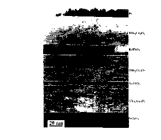
In FIG. 6a, a TEM image of the heterostructure. For the
-25-
CA 02264724 1999-03-01
21008
WO 9~/OW3J PCr/DE97/01~57
investigation by means of transmission electron microscopy
(TEM), there is shown a thin heterostructure layer sequence
according to the invention produced on an SrTiO3 sub~trate and
which is comprised of the following layers: -
Layer 1 35nm YBa2Cu3O7Z
Layer 2 4-Snm BaTbO3
Layer 3 35nm YBa2Cu3O72
Layer 4 12nm BaTbO3
Layer 5 35nm YBa2Cu3O7z
The following is also an outgrowth of the TEM invest-
igation of such a layer sequence according to the invention:
An epitactic growth of all growth is established, whereby
the YBa2Cu3O7z grows advantageously exclusively with a c-axis-
orientation and the BaTbO3 only with (100) orientation. The
result is an experimentally demonstrated heteroepitactic layer
sequence with BaTbO3 and the YBa2Cu3O7z.
At the boundary interfaces, there are no extrinsic phases
and no defect oriented regions. Especially no a-axis growth
and no regions rotated by 45O in the layer plane are observed.
Because of the 10% lattice defect matching of BaTbO3 to the
YBa2Cu3O7z, it is probable that, as with MgO with a similarly
high lattice defect matching, large angle grain limits with
regions rotated by 45O in the layer plane and strong
dislocations of the lattice in the regions of a higher dense
.
CA 02264724 1999-03-01
21008
WO 911/09~ PCT/DE97/01~5~
crosslinking can arise. This, however, has not been observed
a8 the re~ults of FIG. 6b show.
Between the respective BaTbO3 and YBa2Cu3O7z layer there i~
practically an atomically sharp 6A thick intermediate layer
with a non-commensurable structure in which the atomic
spacings are variable and thus stresses of the lattice defect
matching are substantially localized and eliminated at the
boundary interface (FIG. 6b).
This intermediate layer probably is comprised of an oxygen
deficient double layer in which cations of variable valents
like Tb+3/+4 and Cu+l~+2~+3 are distributed. In this connection,
it has been found that in the layer sequence of the invention
neither in the BaTbO3 layer nor in the Yba2Cu3O7z layer do
noticeable lattice defects arise at a spacing from the
boundary layer of less than 1 nm (FIG. 6b).
Because of the incorporation of the intermediate layer and
variations of the atomic spacing in the layer sequence, the
lattice stresses which arise by the combination of the
YBa2Cu3O7z with BaTbO3 are eliminated.
As a consequence, it is not required to reduce the oxygen
conduct in the vicinity of the boundary interface to eliminate
lattice stresses.
As the material for the nonsuperconductive layer in the
layer sequence, there is proposed especially the highly
-27-
CA 02264724 1999-03-01
'21008
WO 9~/0933~ PCT/DE97/01~5~
suitable Perovskitic compound BalxSrxTbO3 whereby the value x
is selected in the range of 0 to 1. The romboidic crystal
structure of this compound can be treated like the pseudo-
cubic Perovskite structure because of its limited deviation
from a cubic structure. This material is indeed known (E.
Paletta, R. Hoppe, Naturwissenschaften 53, 611 (1966) and A.
J. Jacobson, B.C. Tofield, B.E.F. Fender, Acta, Cryst. 828,
956 (1972)). In the literature, however, up to now only the
production of powder specimens has been described. Thin
layers and macroscopic monocrystals of this material have not,
however, been known heretofore. Advantageously this compound
has thermodynamically a comparatively high stability.
With the layer sequence according to the invention it is
found that in spite of the large lattice defect matching of
10%, the microstructure of the YBa2Cu3O7z thin layers which are
grown on the BaTbO3 are not distorted by lattice defects,
extensive misfit dislocations, the growth of extraneous
phases, the growth of a-axis crystals or by crack formation.
These results significantly on the characteristics of the
BaTbO3 whose boundary interfaces to the high temperature
superconductor from the above described intermediate layer,
since this intermediate layer contributes substantially to the
elimination of the lattice stresses and in this manner
prevents lattice disruptions in the superconductor.
-28-
CA 02264724 1999-03-01
21008
WO #/0933~1 PCT/DE9~ S7
It has been found that, with respect to the
characteristics of the intermediate layer, it is advantageous
that Tb ions and/or Cu ions are involved and by ~eA~ of their
variable valence, the oxygen content and thus the lattice
spacings in the intermediate layer are variable. Other
Porovskites can also be considered whose ions have variable
valences for the formation of such an intermediate layer at
the boundary interface.
Since the BaTbO3 materially is extremely expensive,
especially BaPrO3 and BaCeO3 can be mentioned since Pr and Ce,
like Tb, can be trivalent or tetravalent. A slight limitation
as to BaCeO3 as such a material arises since the Ce~4 is
substantially more stable than Ce+3 and thus the variability of
the valence of the Ce ion is more strongly limited than is the
case for the Pr and the Tb.
Under the supposition Tb and Cu ions of varible valence
are incorporated in the intermediate layer, other Porovskite
like compounds can be considered, which contain Cu, Tb, Pr or
Ce ions, in combination with materials which include at least
one CuO2 plane in the unit cell, for the formation of the above
described intermediate layer as a boundary interface layer.
Based upon chemical compatibility, BaCeO3 and BaPrO3 are
indeed less suitable candidates for barrier materials in
Josephson junctions since Pr and Ce ions reduce the critical
-29-
CA 02264724 1999-03-01
21008
WO 9~1/0933~ PCT/DE9~
temperature of the high temperature superconductor. ~owever,
these materials are appropriate for example for use in the
formation of a buffer layer. Based upon the above described
structure of the intermediate layer, the chemical binding
forces in this layer is weaker by comparison to those on e~ch
side of the boundary interface. In this way, it is poqsible
to suppress lattice stresses on each side of the boundary
interface even at low temperatures.
The above mentioned results demonstrate further that
BaTbO3 not only can be integrated in an epitactic multilayer
system but also can be used as a barrier material in Josephson
junctions.
Up to now no material other than BaTbO3 with a Porovskite
structure has been known which, when included in a
heterostructure with the microstructure of the YBa2Cu3O7z does
not at the boundary interface, form lattice dislocations,
extensive misfit upsetting, extraneous phases, local a-axis
growth, crack formation or large angle grain boundaries,
characterized by a 45O rotation of the layer regions in the
layer plane.
Only over a region limited to less than 1 nm in thickness
is a slight lattice disruption observable in the
superconductor directly above the aforedescribed intermediate
layer.
-30-
CA 02264724 1999-03-01
21008
WO 9~ PCT/DE97/01~57
Its use as a buffer material on substrates, especially in
combination with high temperature thin layers, is thus
especially suitable. The following con~ideration~ ~hould be
noted:
BaTbO3 can be used as a buffer layer on chemically
noncompatible substrates to act as a diffusion barrier against
substrate ions detrimental to the superconductivity.
Furthermore, its use as a buffer layer on substrates which
have a lattice defect match to the high temperature super-
conductor like, for example, Mgo or Al2O3, is also possible to
avoid undesired stress in the thin films to be grown. In
addition its use is also possible, as a buffer layer on
substrates, like for example silicon, whose thermal expansion
coefficient deviates sharply from that of the thin film to be
grown. Such substrates, without a buffer layer, normally give
rise to crack formation in thin films.
An epitactic heterosystem comprised of BaTbO3/YBa2Cu3O7z
can also be used when two optional materials are to be
connectable which cannot be directly epitactically bonded or
can be epitactically bonded only with severe distortion of the
microstructure, by introducing a buffer layer. Because of the
simple chemical composition and the high thermodynamic
stability of the compound, it is possible to produce
macroscopic substrate monocrystals.
-31-
CA 02264724 1999-03-01
21008
WO 9~1/0933~ PCT/DE9~
Epitactic BaTbO3 thin layers can be produced on SrTiO3 and
Mgo substrates by RF sputtering in pure oxygen at a pressure
in the range of 2 to 4 mbar and these structureq can be
explored by ~?Ans of x-ray defractometry, RBS/channeling with
He ions and transmission electron microscopy.
Apart from this, the following characteristics which are
useful for applications of the layer sequence according to the
invention and the components according to the invention have
been observed:
In the case of a rough underlay, BaTbO3 has a planarizing
[levelling] effect. BaTbO3 advantageously only contains
elements which are compatible with high temperature
superconductors. From the literature it has only been
indicated initially that polycrystalline massive samples of
BaTbO3 are electrically insulating. The epitactic BaTbO3 thin
layers are likewise insulating.
Because the number of materials which BaTbO3 represents as
an improved crystal structure at the interface with high
temperature superconductors from a narrow group and the number
of materials for high temperature superconductors or materials
with similar crystallographic structure to which they are
applicable can be defined, the invention includes also to the
following materials:
(i) BaTbO3;
-32-
.. . . .....
CA 02264724 1999-03-01
'21008
WO 9~1/0933~ PCT/DE97/01115~
(ii) BalxSrxTbO3 with O<x<1;
(iii) LaCul~TbxO3 with O<x<l;
(iv) RCulxTb~O3 with R = Nd, Eu, Sm and O<x<1;
(v) BalxSrxMO3 with M = Tb, Pr, Ce and O<x<1;
(vi) LaCulxMxO3 with Tb, Pr, Ce and O<x<1;
(vii) RCulxMxO3 with R = Nd, Eu, Sm
M = Tb, Pr, Ce and O<x<1;
(viii) RlyNyCulxMxO3 with R= La, Nd, Eu, Sm;
N= Ba, Sr
M = Tb, Pr, Ce and O<x<1 O<y<l;
(ix) R2yNyCulxMxO4 with R= La, Nd, Eu, Sm;
N= Ba, Sr
M = Tb, Pr, Ce and O<x<1 O<y<l;
( x ) All_xA2xBll yB2yO3
with Al = Ba, Sr;
A2 = La, Nd, Eu, Sm, Sr
Bl = Tb, Pr, Ce, Cu;
B2 = y, Yb, Tm, Lu, In, Sc, Sn, Cu
and O<x<l O<y<1
Materials which are chemically compatible with the high
temperature superconductors should especially be the mentioned
materials and material classes with Perovskite like
structures.
-33-
CA 02264724 1999-03-01
21008
WO 9J/09~ PCr/DE97/01~67
The term "high temperature superconductor and material~
with similar crystallographic structure" means substance~ with
at least three different elements in the units cell, two of
which are oxygen and copper. Further, the unit cells should
include at least one CuO2 plane which is characteristic of the
high temperature superconductor.
The protection is intended to encompass also REBa2Cu30,z
compounds wherein RE = Y, Ca, La, Pr, Nd, Sm, Eu, Gd, Tb, Dy,
Ho, Er, Tm, Yb, Lu.
-34-