Note: Descriptions are shown in the official language in which they were submitted.
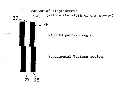
A10152025CA 02264843 1999-03-02-1-SPECIFICATIONPHASE MASK FOR PROCESSING OPTICAL FIBERS,AND ITS FABRICATION METHODART FIELDThe present invention relates generally to a phase maskfor processing optical fibers and its fabrication method, andmore specifically to a phase mask for fabricating adiffraction grating in an optical fiber used for opticalcommunications using ultraviolet laser light, and a method offabricating the same.BACKGROUND ARTOptical fibers have achieved global communication-technology breakthroughs, and enabled highâquality yet large-capacity transoceanic telecommunications. So far, it hasbeen known that a Bragg diffraction grating is prepared in anoptical fiber by providing a periodic index profile in a corealong the optical fiber. By determining the magnitude ofreflectance and the width of frequency characteristics of thediffraction grating depending on the period and length, andthe magnitude of refractive index modulation thereof, thediffraction grating is used for wavelength divisionmultiplexers for optical communication purposes, narrow-bandhigh-reflecting mirrors used with lasers or sensors,wavelength selective filters for filtering out extrawavelengths in fiber amplifiers, etc.However, the wavelength where quartz optical fibers showa minimum attenuation and which is suitable for longâhaul10152025CA 02264843 1999-03-02-2-communication systems is 1.55 pm. To use an optical fiberdiffraction grating at this wavelength, a grating spacing ofabout 500 nm must be needed. Initially, to make such a finestructure in a core has been considered to be in itselfdifficult. Accordingly, some complicated process stepscomprising side polishing, photoresist step, holographyexposure, and reactive ion beam etching are used to make aBragg diffraction grating in an optical fiber core. Muchtime is needed for such processes, resulting in limitedyields.In recent years, however, a method of making adiffraction grating by irradiating an optical fiber withultraviolet radiation for the direct change of a refractiveindex in a core has been known in the art. This ultravioletirradiation method has been steadily put to actual use withthe progress of peripheral technologies due to no need ofcomplex processes.This method using ultraviolet light is now carried outby some processes such as an interference process comprisinginterference of two ray bundles, a writing-perâpoint processwherein a diffraction grating surface is formed one by one byfocusing of a single pulse from an excimer laser), and anirradiation process using a phase mask having a grating,because the grating spacing is as fine as about 500 nm asmentioned above.The interference process comprising interference of tworay bundles offers a problem in connection with the qualityof lateral beams, i.e., spatial coherence, and the writing-10152025CA 02264843 1999-03-02-3-perâpoint process have some operation problems such as theneed of submicron careful step control, and the necessity ofwriting of many surfaces with fine pencils of light.To address the above problems, an irradiation methodusing a phase mask has now received attention. As shown inFig. 7(a), this method uses a phase shift mask 21 obtained byproviding grooves on one side of a quartz substrate at agiven pitch and a given depth. The phase shift mask 21 isthen irradiated with KrF excimer laser light 23 (of 248ânmwavelength) to impart a refractive index change directly to acore 22A of an optical fiber 22, thereby forming a grating.It is here to be noted that reference numeral 22B stands fora cladding of the optical fiber 22. In Fig. 7(a), aninterference pattern 24 in the core 22A is illustrated on anenlarged scale for a better illustration thereof. Fig. 7(b)is a sectional View of the phase mask 21, and Fig. 7(c) is aview illustrating a part of the upper surface of the phasemask 21. The phase mask 21 has a binary phase typediffraction grating structure wherein grooves 26, each havinga depth D, are provided on one surface thereof at arepetitive pitch P, and a strip 27 having substantially thesame width as that of each groove is provided betweenadjacent grooves 26.The depth D (a height difference between strip 27 andgroove 26) of each groove 26 on the phase mask 21 is selectedsuch that the phase of the excimer laser light (beam) 23 thatis exposure light is modulated by a n radian. Zero-orderlight (beam) 25A is reduced to 5% or lower by the phase shift10152025CA 02264843 1999-03-02-4-mask 21, and primary light (beam) leaving the mask 21 isdivided into plus firstâorder diffracted light 25B including35% or more of diffracted light and minus firstâorderdiffracted light 25C. By carrying out irradiation using aninterference fringe at a given pitch determined by the plusfirstâorder diffracted light 25B and the minus firstâorderdiffracted light 25C, the refractive index change at thispitch is imparted to the core of the optical fiber 22.The grating in the optical fiber, fabricated using sucha phase mask 21 as mentioned above, has a constant pitch, andso the grooves 26 on the phase mask 21 used for gratingfabrication, too, have a constant pitch.Such a phase mask is fabricated by preparing patterndata corresponding to a grating form of groove pitch andcarrying out writing with an electron beam writing system toform a grooved grating.In this regard, a chirped grating wherein the gratingpitch increases or decreases linearly or nonlinearlydepending on the position of a grating groove in a directionperpendicular to the grating groove (the repetitive direction jof grating) is now demanded for the Bragg diffraction grating 0to be formed in an optical fiber. Such a grating, forinstance, is used for highâreflecting mirrors having awidened reflection band, and as delay time control means.When such a grating having a grating pitch changinglinearly or nonlinearly depending on the position of groovesin the lengthwise direction of an optical fiber is fabricatedby the interference of plus firstâorder diffracted light and10152025CA 02264843 1999-03-02-5-minus firstâorder diffracted light using a phase mask, it isrequired that the pitch of grooves on the phase mask, too,increase or decrease linearly or nonlinearly in a position-dependent manner, as can be seen from the principle shown inFig. 7(a). The smaller the pitch of grooves on the phasemask, the larger the angle between the plus first-orderdiffracted light and the minus firstâorder diffracted lightand the smaller the pitch of interference fringes. For thefabrication of such a phase mask with an electron beamwriting system, an enormous amount of writing data is neededto write grooves or interâgroove strips all over the range ofthe mask. This often makes mask fabrication difficult.DISCLOSURE OF THE INVENTIONIn View of such problems with the prior art, an objectof the invention is to provide a method of fabricating anoptical fiberâprocessing phase mask which enables a phasemask with a groove pitch changing depending on the positionof grooves in a direction perpendicular to the grooves to beeasily fabricated by electron beam writing, and an opticalfiberâprocessing phase mask fabricated by this method.Another object of the invention is to provide an opticalâfiberâprocessing phase mask with a groove pitch changingdepending on the position of grooves in a groove direction,and a method of fabricating the same by electron beamwriting.According to one aspect of the invention, these objectsare achieved by the provision of an optical fiberâprocessingphase mask comprising on one surface of a transparent10152025CA 02264843 1999-03-02-5-substrate a repetitive pattern of grooves and strips locatedin a grating form, so that an optical fiber is irradiatedwith diffracted light according to said repetitive pattern tomake a diffraction grating in said optical fiber by aninterference fringe of diffracted light of different orders,characterized by juxtaposition of a plurality of patternshaving a linearly or nonlinearly increasing or decreasingpitch, with a constant width ratio between said grooves andsaid strips.In this aspect of the invention, the patterns may bejuxtaposed either in a direction perpendicular to the groovesor in a groove direction.In the latter case, it is preferable that an amount ofdisplacement between a groove in one pattern and a groove inanother pattern adjacent thereto in a direction perpendicularto said grooves is within a width of one groove even athorizontal outermost ends.In the first aspect of the invention, the pattern pitchmay vary between 0.85 pm and 1.25 pm.In the first aspect of the invention, it is preferablethat the height difference between the grooves and the stripson said patterns is of such a magnitude that a phase shift ofapproximately n occurs upon transmission of optical fiber-processing ultraviolet radiation.According to another aspect of the invention, there isprovided a method of fabricating an optical fiberâprocessingphase mask comprising on one surface of a transparentsubstrate a repetitive pattern of grooves and strips located10152025CA 02264843 1999-03-02-7-in a grating form, so that an optical fiber is irradiatedwith diffracted light according to said repetitive pattern tomake a diffraction grating in said optical fiber by aninterference fringe of diffracted light of different orders,characterized in that a plurality of patterns comprisinggrooves and strips at a varying pitch are written in ajuxtaposed relation, thereby fabricating said repetitivepattern of grooves and strips located in a grating form.In this case, the patterns may be written while they arejuxtaposed either in a direction perpendicular to the groovesor in a groove direction.In the latter case, it is preferable that an amount ofdisplacement between the grooves in one pattern and thegrooves in another pattern adjacent thereto in a directionperpendicular to the grooves is within a width of one grooveeven at horizontal outermost ends.In this method of fabricating an optical fiber-processing phase mask, it is preferable that the repetitivepattern of grooves and strips located in a grating form isfabricated by continuously writing grooveâandâstrip patternshaving a varying pitch on the basis of writing dataconcerning a fundamental pattern comprising one groove andone strip while the reduced scale for the writing dataconcerning the fundamental pattern is varied.It is also preferable that the positionâdependent pitchchange of the repetitive pattern of grooves and stripslocated in a grating form is determined depending on a pitchchange of the diffraction grating being made in the optical10152025CA 02264843 1999-03-02-8-fiber, and is caused by a positionâdependent change of thereduced scale for the writing data concerning the fundamentalpattern.The pitch of the repetitive pattern of grooves andstrips located in a grating form, for instance, may varybetween 0.85 pm and 1.25 pm.In the second aspect of the invention, it is preferablethat the height difference between the grooves in therepetitive pattern of grooves and strips located in a gratingform and the strips thereon is of such a magnitude that aphase shift of approximately n occurs upon transmission ofoptical fiber-processing ultraviolet radiation.According to the invention wherein there are juxtaposeda plurality of patterns having a linearly or nonlinearlyincreasing or decreasing pitch, with a constant width ratiobetween grooves and strips, a diffraction grating with avarying pitch can be easily fabricated in an optical fiber.In addition, writing data concerning a fundamental patterncomprising one groove and one strip is multiplied by thereduced scale rate to obtain writing data concerning theoverall repetitive pattern of grooves and strips located in agrating form, which changes in pitch depending on theposition in a direction perpendicular to the grooves or in agroove direction. The amount of writing data can thus begreatly reduced so that patterns can be easily fabricated.Further, this method enables a phase mask to be fabricated atany desired pitch.BRIEF EXPLANATION OF THE DRAWINGSL10152025CA 02264843 1999-03-02-9-Figure l is a top View of the first writing process usedwith the fabrication method of the invention.Figure 2(a) is a schematic of an electron beam writingprocess used for phase mask fabrication, and Figure 2(b) is asectional View of a phase mask.Figure 3 is a top view of the second writing processused with the fabrication method of the invention.Figure 4 is a schematic of an amount of displacementbetween grooves in adjacent regions in the second writingprocess.Figures 5(a) and 5(b) are schematics for illustratingthe writing process according to the invention as comparedwith a prior art writing process.Figures 6(a) to 6(h) are process schematics for oneembodiment of the phase mask fabrication method according tothe invention.Figure 7(a) and 7(b) are schematics for optical fiberprocessing and a phase mask used therewith.BEST MODE FOR CARRYING OUT THE INVENTIONThe optical fiberâprocessing phase mask of theinvention, and the method of fabricating the same will now be 3explained with reference to some embodiments.Fig. 2(b) is a sectional view of a phase mask 21comprising a repetitive alternate pattern of grooves 26 andstrips 27 for making a Bragg diffraction grating in anoptical fiber according to such an arrangement as shown inFig. 7(a). Such a mask 21 is provided thereon with grooves26 and strips 27 as shown in the Fig. 2(a) top view. Here10152025CA 02264843 1999-03-02_]_0_consider the case where grooves 26 are written by exposure toelectron beams in raster scan mode where electron beamscanning lines 28 move along grooves 26 and strips 27 areformed by blanking electron beam scanning, as shown by brokenlines in Fig. 2(a). For exposure of the entire mask 21 toelectron beams, raster scan is carried out in a directionshown by a double arrow in Fig. 2(a). At a position wheregroove 26 is to be written, the mask is actually scanned witha given number of scanning lines (5 lines in the illustratedembodiment), as mentioned above. Then, at a position wherestrip 27.is to be written, as many as scanning lines areblanked. By repetition of this operation, the phase mask 21having a given length is exposed to electron beams.When, according to the invention, the entire mask 21 isexposed to electron beams in the raster scan mode usingelectron beam scanning lines 28, the pitch of groove 26 orstrip 27 is linearly or nonlinearly increased or decreaseddepending on the position of groove 26 in a directionperpendicular to groove 26 or a direction of groove 26. Inthis case, the width of groove 26 is increased or decreaseddepending on such a change. More specifically, while thenumber of scanning lines in the raster scan mode to write onegroove 26 remains unchanged at any position, the inter-central distance of scanning lines 28 is increased ordecreased depending on that change.Fig. 1 is a top view illustrative of the writing processwhere the pitch of grooves 26 or strips 27 is linearly ornonlinearly increased or decreased depending on the position10152025CA 02264843 1999-03-02-11-of grooves 26 in the direction perpendicular to groove 26. Aregion A1 sampled out of the left end of the phase mask 21 hasa groove pitch P1 with respect to groove 26 or strip 27, aregion A2 sampled out of the center of the phase mask 21 has apitch P2 with respect to groove 26 or strip 27, and a regionA3 sampled out of the right end of the phase mask 21 has apitch P3 with respect to groove 26 or strip 27. Here assumeP1 < P2 < P3. The substrate of the phase mask 21 is scannedout sequentially by electron beam scanning lines 28 in theraster scan mode, from top to bottom and from left end toright end, thereby writing each groove 26 thereon. In thiscase, one groove 26 is written by the same number of scanninglines at all regions A1, A2 and A3 (5 scanning lines in theillustrated embodiment). At the position where strip 27 isto be written, as many as scanning lines are blanked. Forthis reason, the interâcentra1 distance of the scanning lines28 changes with regions A1, A2 and A3 depending on pitches P1,P2 and P3 .when such a writing process is used, there is apossibility that unexposed portions may remain afterdevelopment of an electron beam resist (see Fig. 6), because ythe areas of the portions between the scanning lines 28 andunexposed to electron beams to write grooves 26 vary withregions A1, A2 and A3. However, this offers no problem atall, because the unexposed resist is actually removed uponâdevelopment of the regions corresponding to the scanninglines 28.10152025CA 02264843 1999-03-02-12-As explained above, the pitch of grooves 26 or strips 27on the phase mask 21 is linearly or nonlinearly increased ordecreased depending on their position in the directionperpendicular to the grooves 26, so that the width of grooves26 or strips 27 can be increased or decreased depending onsuch a change. By use of the writing process where onegroove 26 is written in the raster scan mode using the samenumber of scanning lines at any position, it is possible towrite the desired pattern all over the surface of thesubstrate of the phase mask 21 with electron beams. Thewriting data needed for this are only two, i.e., fundamentalpattern data concerning one pitch of the mask 21, and areduced scale variation function for the fundamental patterndata, which corresponds to a pitch variation functiondepending on the position of groove 26 in the directionperpendicular to the groove 26.Fig. 3 is a top View of the writing process wherein thepitch of grooves 26 or strips 27 are linearly or nonlinearlyincreased or decreased depending on their position in adirection of each groove 26. An region B1 of a phase mask(21) substrate at its lowermost end along the direction ofgroove 26 has a pitch P1 with respect to groove 26 or strip27, a region B2 positioned just above B1 along the directionof groove 26 has a pitch P2 with respect to groove 26 or strip27, a region B3 positioned just above B2 along the directionof groove 26 has a pitch P3 with respect to groove 26 or strip27, ---, a region B7 of the phase mask (21) substratepositioned just below its uppermost end along the direction10152025CA 02264843 1999-03-02-13-of groove 26 has a pitch P7 with respect to groove 26 or strip27, and a region B8 at the uppermost end along the directionof groove 26 has a pitch P3 with respect to groove 26 or strip27. Here assume P1 > P2 > P3 > --- > P7 > Pg. One region Bn(n = 1 to 7) is scanned with electron beams in the rasterscan mode, from top to bottom, to write groove 26 thereon.Then, the next region Bn+1 is scanned in the same manner asmentioned. In this way, all regions B1 to B8 are scanned towrite grooves 26 thereon. It is here to be understood thatat all regions B1 to Be, one groove 26 is written with thesame number of scanning lines (5 scanning lines in theillustrated embodiment). At a position where strip 27 is tobe written, the same number of scanning lines are blankedduring scanning. For this reason, the inter-central distanceof the scanning lines 28 varies with regions B1 to B3depending on pitches P1 to P3.When such a writing process is used, there is apossibility that unexposed portions may remain afterdevelopment of an electron beam resist (see Fig. 6), becausethe areas of the portions between the scanning lines 28 andunexposed to electron beams to write grooves 26 vary withregions B1 to B8. However, this offers no problem at all,because the unexposed resist is actually removed upondevelopment of the regions corresponding to the scanninglines 28.As explained above, the pitch of grooves 26 or strips 27on the phase mask 21 is linearly or nonlinearly increased ordecreased depending on their position in the direction10152025CA 02264843 1999-03-02-14-perpendicular to grooves 26, so that the width of grooves 26or strips 27 can be increased or decreased depending on sucha change. By use of the writing process where one groove 26is written in the raster scan mode using the same number ofscanning lines at any position, it is possible to write thedesired pattern all over the surface of the substrate of thephase mask 21 with electron beams. The writing data neededfor this are only two, i.e., fundamental pattern dataconcerning one pitch of the mask 21, and a reduced scalevariation function for the fundamental pattern data, whichcorresponds to a pitch variation function depending on theposition of groove 26 in the direction perpendicular to thegroove 26.The phase mask 21 where the pitch of grooves 26 orstrips 27 is linearly or nonlinearly increased or decreaseddepending on their position in the direction of grooves 26,as shown in Fig. 3, is suitable for the fabrication of agrating used to make a Bragg diffraction grating in anoptical fiber, wherein the pitch thereof is linearly ornonlinearly increased or decreased depending on the grooveposition in the groove direction. Such a grating, forinstance, is preferably used to allow the reflectionwavelength of an optical fiber to vary in a position-dependent manner. The grooves 26 and strips 27 on such aphase mask 21 extend in a direction perpendicular to thesheet surface on which Fig. 7(a) is drawn, so that the pitchof the grating to be fabricated in an optical fiber 22 can beselectively controlled by control of the position of the-CA 02264843 1999-03-02. . -15-grooves and strips in the direction perpendicular to thesheet surface.In the writing process shown in Fig. 3, the abovereduced scale variation function should be set such that the5 amount of displacement between groove 26 on one region Bn andgroove 26 on the next region Bn+1 in the directionperpendicular to groove 26 is within the width of one groove26 even at the horizontal outermost ends, as shown in Fig. 4.Although it is acceptable that writing is carried out while10 one region Bn is in Contact with the adjacent region Bn+1, itis preferable that both the regions overlap to some extentbecause the grooves 26 or straps 27 are smoothly joined toeach other.Fig. 5 is a schematic illustrating the writing process15 of the invention as compared with a prior art writingprocess. Fig. 5 corresponds to the writing process in Fig.1, and corresponds nearly to the writing process in Fig. 3 aswell. When the pitch of grooves 26 or strips 27 on the phasemask 21 are linearly or nonlinearly increased or decreased in20 a positionâdependent manner, the prior art writing processrequires an enormous amount of writing data, and so a numberof writing pattern data A, B, C, D, E, -~-, V, W, X, Y and Z,as shown in Fig. 5(b), must be kept on hand. This iscontrast to the writing process of the invention, for which25 only fundamental pattern data A is needed together with areduced scale variation function ï¬(x) corresponding to aposition x (the position of groove 26 in the directionperpendicular to groove 26 in Fig. 1, and the position of10152025CA 02264843 1999-03-02-15-groove 26 in the direction of groove 26 in Fig. 3). Forwriting, only the use of A X B(x) = An and the fundamentalpattern data A scaled down depending on the position isneeded, as shown in Fig. 5(a). Thus, the amount of writingdata can be reduced so that writing can be facilitated. InFig. 1 and Fig. 5(a), the writing range in the verticaldirection varies with position because the reduced scale isvaried not only in the horizontal direction but in thevertical direction as well. When the reduced scale is variedin the horizontal direction alone depending on the position(as required in Fig. 3 in particular), the writing range inthe vertical direction can be kept constant at everyposition.For instance, when oneâpitch writing data comprising a0.125âpm address unit and 10 scanning lines are provided asthe fundamental pattern data, the reduced scale is given by(desired grating pitch)/(0.125 x 10). Using this reducedscale and the fundamental pattern data with an electron beamwriting system, grooves are written on an electron beamresist coated on the transparent substrate. One specificembodiment of the phase mask fabrication method of theinvention using such a writing process will now be explained.Figs. 6(a) to 6(h) are sectional views of steps offabricating a phase mask according to the invention. Here,reference numeral 10 stand for a phase mask blank, 11 aquartz substrate, 12 a chromium thin film, 12A a chromiumthin film pattern, 12B a chromium thin film opening, 13 anelectron beam resist, 13A a resist pattern, 13B a resist10152025CA 02264843 1999-03-02-17-opening, 14 an electron beam, 21 a phase mask, 26 a groove,and 27 a strip.As shown in Fig. 6(a), the chromium thin film 12 of 150A in thickness was first formed on quartz substrate 11 toprepare the blank 10. The chromium thin film 12 is useful toprevent chargingâup during irradiation of electron beamresist 13 with electron beams 14 at the later step, and actsas a mask in making grooves 26 in the quartz substrate. Thethickness of chromium thin film 12 is also important in viewof resolution upon chromium thin film etching, and so ispreferably in the range of 100 to 200 h.Then, the electron resist 13, e.g., an electron resistRE5100P (made by Hitachi Kasei K.K.) was coated on chromiumthin film 12 to a thickness of 400 nm and dried, as shown inFig. 6(b).Following this, an electron beam writing system MEBESIII(made by ETEC) was used to expose electron beam resist 13 toelectron beams 14 at an exposure of 1.2 pC/cmz, as shown inFig. 6(c), while, as explained with reference to Figs. 1 and3, the pitch of grooves 26 was linearly increased, from leftto right or in a direction perpendicular to the drawingsheet, depending on their position in the directionperpendicular to grooves 26 or their position in thedirection of grooves 26, and the widths of grooves 26 andstrips 27 were increased with such a change. In this step,the width between the electron beams 14 was sequentiallycontrolled in such a way that one groove was always written10152025CA 02264843 1999-03-02-18-with five scanning lines at every position in the raster scanmode.After exposure to the electron beams, baking (postexposure baking or PEB) was carried out at 90°C for 5minutes. Thereafter, the electron beam resist 13 wasdeveloped with TMAH (tetramethylammonium hydroxide) at aconcentration of 2.38% to form such a desired resist pattern13A as shown in Fig. 6(d). It is here to be noted that thepost exposure baking (PEB) was performed to selectivelyenhance the sensitivity of the portions irradiated withelectron beams 14.Subsequently, dry etching was carried out using a CH2Cl2gas while the resist pattern 13A was used as a mask to formsuch a chromium thin film pattern 12A as shown in Fig. 6(e).As shown in Fig. 6(f), the quartz substrate 11 was thenetched to a depth of exactly 240 nm using a CF4 gas while thechromium thin film pattern 12A was used as a mask. Depthcontrol was carried out by control of etching time, andetching could be performed while the thickness was controlledto the range of 200 to 400 nm.After this, the resist pattern 13A was stripped out withâsulfuric acid of 70°C, as shown in Fig. 6(g). Then, thechromium thin film pattern 12A was etched out with anammonium solution of cerium (IV) nitrate, as shown in Fig.6(h). Finally, the product was washed to obtain a finishedline-andâspace (or strip 27âandâgroove 26) phase mask 21having a depth of 240 nm and a pitch changing linearly from10152025CA 02264843 1999-03-02-19-0.85 pm to 1.25 pm in the direction perpendicular to grooves26 or in the direction of grooves 26.While the optical fiberâprocessing phase mask and itsfabrication method have been explained with reference to somepreferred embodiments, it is to be understood that theinvention is in no sense limited thereto and so manymodification may be made thereto. While the invention hasbeen explained with reference to the raster scan typeelectron beam writing system, it is also to be understoodthat the invention may be carried out using a vector scan orother type electron beam writing system.POSSIBILITY OF UTILIZATION IN INDUSTRYAs can be obvious from the foregoing explanation, theoptical fiberâprocessing phase mask of the invention and itsfabrication method enable a diffraction grating with avarying pitch to be made in an optical fiber. This isbecause the phase mask of the invention comprises a pluralityof juxtaposed patterns, each having a linearly or nonlinearlyincreasing or decreasing pitch, with a constant width ratioof grooves and strips. If writing data concerning afundamental pattern comprising one groove and one strip aremultiplied by a reduced scale ratio, it is then possible toobtain writing data concerning the entire repetitive patternof grooves and strips located in a grating from with a pitchvarying depending on their position in the directionperpendicular to grooves or in the direction of grooves.Thus, some considerable reductions in the amount of writingdata are achieved to make pattern formation easy. ThisCA 02264843 1999-03-02-20-process also enables a phase mask to be fabricated at anydesired pitch.