Note: Descriptions are shown in the official language in which they were submitted.
CA 02266227 1999-03-22
1
OPTICAL TRANSMISSION SYSTEM INCLUDING OPTICAL
RESTORATION
Technical Field
This invention relates to restoration of transmission systems and, more
particularly, to restoration of optical transmission systems.
Background of the Invention
Optical transmission systems and, especially, those employing Dense Wavelength
Division Multiplexing (DWDM) are desirable because they provide extremely wide
bandwidths for communications channels. Each communications channel in the
DWDM
to transmission system carries a plurality, for example, 16, 40 or even 80,
optical channels
(wavelengths) on a single optical fiber and single optical repeater. However,
there is a
trade off between providing wider bandwidth communications channels, with
their
corresponding lower cost of transport, and their vulnerability to large-scale
disruption of
communications services because of transmission medium failure. Therefore, the
ability
of an optical transmission system, for example, those employing DWDM, to
restore itself
after a transmission medium failure is very important because of its wider
impact on
communications services. The DWDM optical transmission systems are of
particular
interest because of their restoration capabilities.
Prior attempts at providing adequate restoration in optical transmission
systems
2o have focused on so-called 1 + 1 optical protection switching and on optical
cross
connect systems. The 1 + 1 optical protection switching is limited in its
application and
does not efficiently use optical fiber. Known optical cross connect systems,
require the
use of a relatively large optical switching fabric to accommodate the capacity
of the
optical transmission system. Unfortunately, current technology may not support
providing such a large switching fabric having an acceptable optical
performance level.
Moreover, use of such a large switching fabric in the optical cross connect
comes with a
relatively high cost. Furthermore, the optical cross connect system will be
slower in
terms of restoration speed than provided by prior known SONET/SDH ring
transmission
CA 02266227 1999-03-22
~ 2
systems. In order to protect all wavelengths used in the optical transmission
system the
prior arrangements had to switch one wavelength at a time. Such switching is
very
inefficient.
Summary of the Invention
These problems and other limitations of prior known optical restoration
systems
are overcome in an optical communications system that employs a plurality of
optical
nodes interconnected in an optical ring transmission configuration by at least
two optical
transmission media, for example, optical fiber. The at least two optical
transmission
media, in this example, provide optical service transmission capacity and
optical
1o protection transmission capacity. Efficient restoration of optical
communications
between optical nodes in the ring, after an optical transmission media
failure, is realized
by employing a relatively simple and efficient optical switch matrix having a
first number
of possible switching states and, then, by utilizing only a second number of
the switching
states fewer than the first number to switch optically from the optical
service
transmission capacity of the failed or faulted optical transmission media to
the optical
protection transmission capacity of another optical transmission media.
Optical
switching states of the optical switch matrix are blocked that are not
actively used for
switching from the active optical service capacity of the faulted optical
transmission
media to the standby optical protection capacity of the other optical
transmission media.
2o Use of this relatively simple optical switch matrix allows for the bulk
switching of the
optical wavelengths as contrasted with the one-to-one switching of the optical
wavelengths used in prior arrangements.
In a preferred embodiment of the invention, each of the at least two optical
transmission media provides both bi-directional optical service transmission
capacity and
bi-directional optical protection transmission capacity. In a specific
embodiment of the
invention, each optical transmission channel (wavelength) includes 50 percent
bi-
directional optical service transmission capacity and 50 percent bi-
directional optical
protection transmission capacity.
CA 02266227 2003-04-02
3
In another embodiment of the invention, one of the at least two optical
transmission media provides active optical service transmission capacity and
another
of the optical transmission media provides standby optical protection
transmission
capacity.
In still another embodiment of the invention, at least four optical
transmission
media (optical fiber) are utilized to provide transmit and receive active
optical service
transmission capacity and transmit and receive standby optical protection
transmission capacity. Specifically, one pair of the optical transmission
media is used
to provide bi-directional transmit and receive active optical service
transmission
1o capacity and another pair of the optical transmission media is used to
provide the
bi-directional transmit and receive standby optical protection transmission
capacity.
In accordance with one aspect of the present invention there is provided a
controllable optical switch matrix for use in an optical node intended to be
connected
with a plurality of optical nodes in an optical transmission ring
configuration and the
controllable switch matrix intended for use in an optical node to interface
with
terminal equipment including a plurality of optical inputs and a plurality of
optical
outputs, the controllable optical switch matrix comprising: a plurality of
optical
inputs to which incoming optical signals are intended to be supplied; a
plurality of
optical outputs to which outgoing optical signals are intended to be supplied;
wherein
2o said controllable optical switch matrix has a first predetermined number of
possible
optical switching states, and at least first and second of said optical switch
matrix
optical inputs being directly optically connected in a predetermined fixed one-
to-one
optical connection relationship to at least first and second of said optical
switch
matrix optical outputs, respectively, thereby being at least first and second
predetermined fixed optical connections effecting at least first and second of
said
optical switch matrix switch states, said first optical input of said optical
switch
matrix being directly optically connected to a first optical output of the
terminal
equipment and intended to transport optical signals to said first optical
output of said
optical switch matrix in a first direction of transmission, and said second
optical input
of said optical switch matrix being directly optically connected to a second
optical
CA 02266227 2003-04-02
3a
output of the terminal equipment and intended to transport optical signals to
said
second optical output of said optical switch matrix in a second direction of
transmission opposite to said first direction of transmission; and a plurality
of
controllable optical switch units being responsive to switch control signals
for
controllably optically connecting prescribed ones of said inputs to prescribed
ones of
said outputs and being limited to switching of only a second number of said
optical
switching states fewer in number than said first predetermined number of
optical
switching states.
In accordance with another aspect of the present invention there is provided
an
to optical node for use in an optical transmission system including a
plurality of optical
nodes connected by at least two optical transmission media in an optical
transmission
ring configuration, the at least two optical transmission media providing
active optical
service transmission capacity and standby optical protection transmission
capacity,
the node comprising: terminal equipment including a plurality of optical
inputs and a
plurality of optical outputs; a controllable optical switch matrix having a
plurality of
optical inputs to which incoming optical signals are intended to be supplied,
a
plurality of optical outputs to which outgoing optical signals are intended to
be
supplied, a first predetermined number of possible optical switching states
between
said optical switch matrix optical inputs and optical outputs, at least first
and second
of said optical switch matrix optical inputs being directly optically
connected in a
predetermined fixed one-to-one optical connection relationship to at least
first and
second of said optical switch matrix optical outputs, respectively, thereby
being at
least first and second predetermined fixed optical connections effecting at
least first
and second of said optical switch matrix switch states, said first optical
input of said
optical switch matrix being directly optically connected to a first optical
output of the
terminal equipment and intended to transport optical signals to said first
optical output
of said optical switch matrix in a first direction of transmission, and said
second
optical input of said optical switch matrix being directly optically connected
to a
second optical output of the terminal equipment and intended to transport
optical
3o signals to said second optical output of said optical switch matrix in a
second
direction of transmission opposite to said first direction of transmission,
and a
CA 02266227 2003-04-02
3b
plurality of controllable optical switch units being responsive to control
signals for
controllably switching optical signals between the optical service capacity
and optical
protection capacity of said at least two optical transmission media and being
limited
to optically switching of only a second number of said optical switching
states fewer
in number than said first predetermined number of optical switching states; an
optical
detector for detecting failure of any of said at least two optical
transmission media and
for generating an indication of such failure; and a controller responsive to
an
indication of an optical transmission media failure from said optical detector
for
generating said control signals to be supplied to said optical switch units in
said
1 o optical switch matrix.
In accordance with yet another aspect of the present invention there is
provided an optical transmission system including a plurality of optical nodes
connected in a ring configuration by at least two optical transmission media
in a first
direction of transmission and at least two optical transmission media in a
second
direction of transmission, each of the optical nodes comprising: terminal
equipment
including a plurality of optical inputs and a plurality of optical outputs; a
controllable
optical switch matrix having a plurality of optical inputs to which incoming
optical
signals are intended to be supplied, a plurality of optical outputs to which
outgoing
optical signals are intended to be supplied, a first predetermined number of
possible
optical switching states between said optical switch matrix optical inputs and
optical
outputs, at least first and second of said optical switch matrix optical
inputs being
directly optically connected in a predetermined fixed one-to-one optical
connection
relationship to at least first and second of said optical switch matrix
optical outputs,
respectively, thereby being at least first and second predetermined fixed
optical
connections effecting at least first and second of said optical switch matrix
switch
states, said first optical input of said optical switch matrix being directly
optically
connected to a first optical output of the terminal equipment and intended to
transport
optical signals to said first optical output of said optical switch matrix in
a first
direction of transmission, and said second optical input of said optical
switch matrix
3o being directly optically connected to a second optical output of the
terminal
equipment and intended to transport optical signals to said second optical
output of
CA 02266227 2003-04-02
3c
said optical switch matrix in a second direction of transmission opposite to
said first
direction of transmission, and a plurality of controllable optical switch
units being
responsive to control signals for controllably switching optical signals
between the
optical service capacity and optical protection capacity of said at least two
optical
transmission media and being limited to optically switching of only a second
number
of said optical switching states fewer in number than said first predetermined
number
of optical switching states; an optical detector for detecting failure of any
of said at
least two optical transmission media and for generating an indication of such
failure;
and a controller responsive to an indication of an optical transmission media
failure
1 o from said optical detector for generating said control signals to be
supplied to said
optical switch units in said optical switch matrix.
Brief Description of the Drawings
FIG. 1 illustrates, in simplified block form, details of an optical ring
transmission system;
FIG. 2 illustrates, in simplified block diagram form, details of an optical
node
used in the system of FIG. l and including an embodiment of the invention;
FIG. 3 illustrates, in simplified block diagram form, details of another
version
of an optical node that can be used in the system of FIG. 1 and including an
embodiment of the invention;
2o FIG. 4 illustrates, in simplified block diagram form, an optical node
especially
suited for a four optical fiber system and including an embodiment of the
invention;
FIG. 5 illustrates, in simplified block diagram form, details of applicants'
unique optical switch matrix employed in an embodiment of their invention;
FIG. 6 is a state diagram showing the allowable optical switching states of
the
optical switching matrix of FIG. 5 for both terminal optical nodes and
intermediate
pass through optical nodes;
CA 02266227 1999-03-22
- 4
FIG. 7 is a flow chart showing the operation of an optical node in response to
a
detected optical transmission media failure;
FIG. 8 illustrates, in simplified block diagram form, details of an optical
node
effecting an optical protection switch in response to a transmission media
failure on the
east side of the optical node;
FIG. 9 is a state diagram showing the optical switch states for effecting the
optical protection switch in the optical node of FIG. 8;
FIG. 10 illustrates, in simplified block diagram form, details of an optical
node
effecting an optical protection switch in response to a transmission media
failure on the
1o west side of the optical node;
FIG. 11 is a state diagram showing the optical switch states for effecting the
optical protection switch in the optical node of FIG. 10;
FIG. 12 illustrates, in simplified block diagram form, details of an optical
node
effecting a pass through optical protection switch in response to a
transmission media
failure;
FIG. 13 is a state diagram showing the optical switch states for effecting the
pass
through optical protection switch in the optical node of FIG. 12;
FIG. 14 shows, in simplified block form, a plurality of optical nodes
connected in
a ring configuration and the optical switch matrix connections in each of the
optical
2o nodes for normal operation;
FIG. 15 shows, in simplified block form, a plurality of optical nodes
connected in
a ring configuration and the optical switch matrix connections in each of the
optical
nodes for effecting an optical protection switch in response to a transmission
media
failure; and
FIG. 16 shows, in simplified block diagram form, details of optical monitor
206
of FIG. 2.
' CA 02266227 1999-03-22
_ 5
Detailed Description
FIG. 1 shows, in simplified form, bi-directional optical transmission system
100,
which connected in a ring configuration. For brevity and clarity of exposition
optical
transmission system 100 is shown as including only optical nodes 101 through
104, each
incorporating an embodiment of the invention. Optical nodes 101 through 104
are
interconnected by bi-directional optical transmission media 110, which for
brevity and
clarity of exposition, in this example, transport active service transmission
capacity and
by bi-directional optical transmission media 120, which also for brevity and
clarity of
exposition, in this example transports standby protection transmission
capacity. In this
1o example, optical transmission medium 110 and 120 are comprised of optical
fibers and
each could be comprised of a single optical fiber or two (2) optical fibers.
That is, bi-
directional optical transmission system 100 could be either a two (2) optical
fiber or a
four (4) optical fiber system. In a preferred embodiment of the invention, two
(2) optical
fibers are employed, each of the optical fibers ideally including 50% service
bandwidth
and 50% protection bandwidth. In an alternative embodiment of the invention,
one of the
two (2) optical fibers can carry active service transmission capacity and the
other optical
fiber can carry standby protection transmission capacity. In a four (4)
optical fiber
system, separate optical fibers are employed to transport active service
transmission
capacity in both directions of transmission, and separate optical fiber are
employed to
2o transport standby protection transmission capacity in both directions of
transmission.
The optical transmission system 100 could transport, for example, 8, 16, 32,
40, 80, etc.
communications channels, i.e., wavelengths. It should be noted that in either
the two (2)
optical fiber arrangement or the four (4) optical fiber arrangement a separate
so-called
telemetry channel is employed as a maintenance channel, in addition to the
communications channels. Thus, in an eight (8) channel system, nine (9)
channels are
transported, in a 16 channel system, 17 channels are transported and so on.
The
maintenance channel transports, among other things, the switching information
for
configuring optical nodes 101 through 104 in optical transmission system 100.
Use of
the maintenance channel in transporting protection switching information in
order to
restore transmission in optical transmission system 100 in response to a
transmission
' CA 02266227 1999-03-22
6
media failure or the like is described below. Two (2) and four (4) optical
fiber
transmission systems are known.
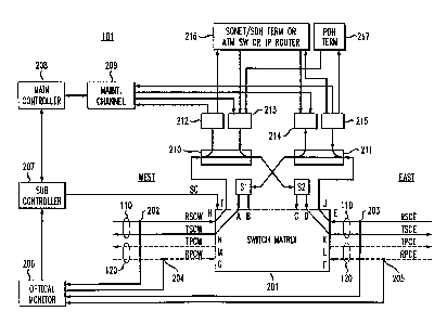
FIG. 2 shows, in simplified block diagram form, details of optical nodes 101 -
104, including an embodiment of the invention and operating in a normal
transport
mode. That is, there is no optical transmission media failure or other
disruption of
transmission service. Again, for brevity and clarity of exposition, the bi-
directional
active service transmission capacity is shown as being transported on optical
transmission media 110 and the standby protection transmission capacity is
shown as
being transported on optical transmission media 120. As indicated above, in a
preferred
to embodiment of the invention, each of at least two optical fibers transports
both active
service transmission capacity and standby protection transmission capacity.
Shown is
optical receive service capacity from the west (RSCW) being supplied to input
H of
applicants' unique optical switch matrix 201, optical transmit service
capacity to the west
(TSCW) being supplied from output N of optical switch matrix 201, optical
transmit
protection capacity to the west (TPCW) being supplied from output M of optical
switch
matrix 201, and optical receive protection capacity from the west (RPCV~ being
supplied to input G of optical switch matrix 201. Similarly, on the east side
of optical
node 101, optical receive service capacity (RSCE), is supplied to input E,
optical
transmit service capacity (TSCE) is supplied from output K, optical receive
protection
2o capacity (RPCE) is supplied to input F and optical transmit protection
capacity (TPCE)
is supplied from output L, all to/from optical switch matrix 201. RSCW
supplied to
input H is supplied via optical switch matrix 201 to output I and, thereafter,
to optical
add/drop multiplexer 210. Similarly, RSCE supplied to input E is supplied via
optical
switch matrix 201 to output J and, thereafter, to optical add/drop multiplexer
211.
TSCW from optical add/drop multiplexer 211 is supplied to optical sputter S 1,
which
forms two versions of it. One version of TSCW is supplied to input A and,
thereafter, to
output N of optical switch matrix 201, while the other version of TSCW is
supplied to
input B for use.if a protection switch is required. Similarly, TSCE from
optical add/drop
multiplexer 210 is supplied to optical sputter S2, which forms two versions of
it. One
3o version of TSCE is supplied to input D and, thereafter, to output K of
optical switch
CA 02266227 1999-03-22
_ 7
matrix 201, while the other version of TSCW is supplied to input C for use if
a
protection switch is required. Control signals (SC) for controlling operation
of optical
switch matrix 201 are supplied from sub controller 207. Details of optical
switch matrix
201 and its operation are described below.
A relatively small portion of optical energy (for example, less than 2%) being
transported via each of RSCW, RPCE, RPCW and RPCE is coupled via optical taps
202, 203, 204 and 205, respectively, to optical monitor 206. Optical monitor
206
determines whether a loss of signal (LOS) has occurred on any of the optical
transports
supplying optical signals to optical node 101 and, therein, optical switch
matrix 201.
1o Details of optical monitor 206 are described below in relationship to FIG.
16. Any LOS
information is supplied from optical monitor 206 to sub controller 207, which
supplies
switch control (SC) signals to optical switch matrix 201 for effected any
required
protection switch, and to main controller 208. In turn, main controller 208
supplies
switch information, among others, to maintenance channel unit 209. Maintenance
1s channel unit 209 supplies switch information via the maintenance channel to
optical
combining units 213 and 214 where it is combined with other optical channels
(if any) to
be added via add/drop multiplexers 210 and 211 to TSCW and TSCE to transported
to
others of optical nodes 102 through 104 for use in effecting appropriate
protection
switches at those optical nodes. Note if a protection switch is made, then,
the
2o maintenance channel is transported as appropriate via TPCW and/or TPCE.
Incoming
maintenance channel information is supplied from RSCW and RSCE and if a
protection
switch has been made from RPCW and/or RPCE as appropriate, where it is dropped
via
add/drop multiplexers 210 and 211 to optical sputters 212 and 21 S,
respectively. Optical
maintenance channel information is supplied from optical splitters 212 and 21
S to
25 maintenance channel unit 209 and, thereafter, to main controller 208. Then
any
protection switch information being transported on the maintenance channel is
supplied
to sub controller 207 where it is determined whether a protection switch is
required. If a
protection switch is required appropriate switch control (SC) signals are
supplied from
sub controller 207 to optical switch matrix 201. Optical communications
channels
3o dropped by add/drop multiplexers 210 and 211 are also supplied to optical
sputters 212
CA 02266227 1999-03-22
8
and 215, respectively. Optical communications channel information from optical
sputters
212 and 215 is supplied to optical terminal equipment 216 as desired. Terminal
equipment 216 may include, for example, a synchronous optical
network/synchronous
digital hierarchy (SONET/SDH) terminal, or an asynchronous transfer mode (ATM)
switch, or an Internet protocol (IP) router, or the like. Additionally,
optical
communications channel information from optical splitter 215 is supplied to
peizosynchronous digital hierarchy (PDH) terminal 217. Communications channel
information from terminal equipment 216 is supplied to be added for transport
to optical
combining units 213 and 214 and, thereafter, to add/drop multiplexers 210 and
211.
to Optical communications channel information from peizosynchronous digital
hierarchy
(PDH) terminal 217 is supplied to optical combining unit 213 and, thereafter,
to
add/drop multiplexer 210 to be added to TSCE and/or TPSE. Note that the
peizosynchronous digital hierarchy (PDH) communications information from
terminal
217 is span related and, therefore, is only supplied, in this example, to TSCE
and/or
TPCE.
FIG. 3 illustrates, in simplified block diagram form, details of another
version of
an optical node that can be used in optical nodes 1-1 through 104 in the
system of FIG. 1
and including an embodiment of the invention. All elements of the version of
optical
node 101 shown in FIG. 3 that are identical to those, described above,
regarding the
2o version of optical node 101 shown in FIG. 2 have been similarly numbered
and will not
be described again. The differences between the versions of optical node 101
shown in
FIG. 2 and FIG. 3 are that in FIG. 3 optical demultiplexer (DMUX) 301 and
optical
multiplexer (MUX) 302 replace add/drop multiplexer 210, optical sputter 212
and
optical combining unit 213, and optical demultiplexer (DMUX) 303 and optical
multiplexer (MLJX) 304 replace add/drop multiplexer 211, optical splitter 214
and
optical combining unit 215. Otherwise the elements and operation of the
versions of
optical node 101 shown in FIGs. 2 and 3 are identical. It will be apparent to
those
skilled in the art how DMUX 301 and MUX 302, and DMUX 303 and MUX 304 are a
direct substitute for add/drop multiplexer 210, optical sputter 212 and
optical combining
CA 02266227 1999-03-22
9
unit 213, and for add/drop multiplexer 211, optical sputter 214 and optical
combining
unit 215, respectively.
FIG. 4 illustrates, in simplified block diagram form, an optical node
especially
suited for a four optical fiber system and including an embodiment of the
invention. All
elements of the version of optical node 101 shown in FIG. 4 that are identical
to those,
described above, regarding the version of optical node 101 shown in FIG. 2
have been
similarly numbered and will not be described again. The differences between
the
versions of optical node 101 shown in FIG. 2 and FIG. 4 are that in FIG. 4
four (4)
optical fibers are employed to transport the incoming and outgoing optical
signals and,
1o thereby, providing the active transmit and receive service capacity, and
the standby
transmit and receive protection capacity. Thus, separate optical fibers are
employed to
transport each of RSCW, TSCW, TPCW and RPCW. Additionally, terminal equipment
401 includes a four (4) optical fiber ring, or a SONET/DSH terminal or an ATM
switch
or an IP router. Circuit paths are provided from optical sputters 212 and 215
to
equipment 401, and from equipment 401 to optical combining units 213 and 214
to
accommodate the four optical fiber ring, as will be apparent to those skilled
in the art.
FIG. 5 illustrates, in simplified block diagram form, details of applicants'
unique
optical switch matrix, e.g., optical switch matrix 201, employed in an
embodiment of
their invention. Note that in this example inputs A through H and outputs I
through N of
optical switch matrix 201 are optical. Shown in FIG. 5 are optical sputter S 1
dual
feeding optical communications channels normally intended for west bound
transmission
to inputs A and B of optical switch matrix 201, and optical splitter S2 dual
feeding
optical communications channels normally intended for east bound transmission
to inputs
C and D of optical switch matrix 201. In this example, it is noted that input
A is
connected directly to output N in the west bound direction, and that input D
is
connected directly to output K in the east bound direction. Of course, these
"direct"
connections can be made in any of a number of ways, for example, they can be
made by
assigning optical switch units to erect the desired connections at system
setup, or
dynamically in response to control signals These "direct" connections
significantly
3o simplify optical switch matrix 201 and make it significantly more
efficient. Optical
CA 02266227 1999-03-22
switch matrix 201 is further comprised of controllable optical switches 501
through 507.
Optical switches SO1 through 507 are controlled via switch control (SC)
signals from sub
controller 207 (FIG. 2) to effect the bulk switching of optical signals
including
communications channels being supplied to them. This bulk optical switching is
an
5 important feature of applicants' unique optical switch matrix because it
more efFlciently
effects switching of the optical signals. Again, note that switching with
prior known
arrangements was on an optical channel-by-optical channel basis, which is
significantly
less efficient than applicants' use of bulk switching. It should be further
noted that
although optical switch matrix 201 has eight (8) inputs and six (6) outputs,
only 10
1o switching states are allowed of which two (2) switching states are
designated by
preassigning the optical input and optical output connections. This
preassignment of two
of the optical switch states may be realized in a number of ways, for example,
permanent
optical connections, optical switches always switched to those optical switch
states, or
the like. Thus, there are effectively only eight (8) allowable switching
states of optical
switch matrix 201, which significantly reduces the complexity of the switching
of the
optical signals and allows the use of relatively simple switching elements
that are readily
available. Indeed, no large complex switching matrix is required as would be
in an
optical channel-by-optical channel switching arrangement or in an optical
cross connect
switch. Further note that two (2) of the allowable optical switching states of
optical
2o switch matrix 201 are employed only in pass through optical nodes.
FIG. 6 is a state diagram showing the allowable switching states of the
optical
switch matrix 201 of FIG. 5 for both terminal optical nodes and intermediate
pass
through optical nodes. Note that the allowable switching states are indicated
by a "dot"
in the middle of a square representative of an allowable switching state, and
a switched
state or preassigned, e.g. a permanently connected, switched state is
indicated by a "X"
in the square representative of the switched state or preassigned state. Thus,
as seen in
FIG. 6, input A is preassigned, i.e., permanently connected, to output N,
input B can be
controllably connected to output L, input C can be controllably connected to
output M,
input D is preassigned, i.e., permanently connected, to output K, input E can
be
3o controllably connected to output J, input F can be controllably connected
to output I or
CA 02266227 1999-03-22
11
output M, input G can be controllably connected to output J or output L and
input H can
be controllably connected to output I, all of optical switch matrix 201 shown
in FIG. 5.
Returning to FIG. 5, the above controllable switching states of simplified
optical
switch matrix 201, are realized by employing controllable optical switching
units 501
through 507. To this end, inputs H and F are supplied to individual inputs of
optical
switching unit 501. Inputs E and G are supplied to individual inputs of
optical switching
unit 502. Inputs B and C are supplied to individual inputs of optical
switching unit 503.
One output of optical switching unit 501 is supplied to an input of optical
switching unit
504. Consequently, an optical signal supplied via either input H or input F
can be
to controllably supplied to output I via optical switching units 504 and SO1,
in response to
control signals SC. One output of optical switching unit 502 is supplied to an
input of
optical switching unit 505. Consequently, an optical signal supplied via
either input E or
input G can be controllably supplied to output J via optical switching units
505 and 502,
in response to control signals SC. Another output from optical switching unit
501 is
supplied to one input of optical switching unit 507, and an output from
optical switching
unit 503 is supplied to another input of optical switching unit 507.
Consequently, an
optical signal supplied via either input C or input F can be controllably
supplied to output
M via optical switching units 507, SO1 and 503, in response to control signals
SC.
Another output from optical switching unit 502 is supplied to one input of
optical
2o switching unit 506, and another output from optical switching unit 503 is
supplied to
another input of optical switching unit 506. Consequently, an optical signal
supplied via
either input B or input G can be controllably supplied to output L via optical
switching
units 506, 502 and 503, in response to control signals SC.
FIG. 7 is a flow chart showing the operation of main controller 208 of an
optical
node, in response to a detected optical transmission media failure. The
process is started
in step 701 in response to a failure indication from sub controller 207. Step
702
indicates that optical monitor 206 has indicated a failure. Then, step 703
starts a so-
called millisecond (msec) counter clock. Step 704 tests to determine if a
predetermined
threshold time interval in step 703. If the test result in step 704 is NO,
step 705 resets
3o the counter of step 703, and control is returned to step 703. Thereafter,
steps 703, 704
CA 02266227 1999-03-22
12
and 705 are iterated unit step 704 yields a YES result and control is
transferred to step
706. Step 706 causes instructions to be sent via the maintenance channel to
other optical
nodes in the optical ring communications system including appropriate optical
switch
states. Then, step 707 starts a millisecond (msec) counter clock. Step 708
tests to
s determine if confirmation is received via the maintenance channel that the
switching of
the switch states sent in step 706 have been completed within a predetermined
time out
interval, T, as indicated by the counter in step 707. If the test result in
step 708 is NO,
step 709 stops the switching process because the attempt at restoration has
failed. If the
test result in step 708 is YES, step 710 indicates that the optical
transmission system
1o restoration has been completed.
FIG. 8 illustrates, in simplified block diagram form, details of an optical
node,
e.g., 101, effecting an optical protection switch in response to a
transmission media
failure on the east side of the optical node. Upon optical detector 206
detecting the
failure, sub controller 207 sends optical switch control signals SC to optical
switch
15 matrix 201 and to main controller 208. Optical switch matrix 201 effects
the optical
switch indicated in dashed outline. That is, input C is controllably connected
to output
M and input G is controllably connected to output J. Note that input H remains
connected to output I, and the preassigned, i.e., permanent, optical
connections of input
A to output N and input D to output K remain intact. FIG. 9 is a state diagram
showing
2o the optical switch states, indicated by "X", for effecting the optical
protection switch in
the optical node of FIG. 8. Main controller 208 transmits instructions, via
the
maintenance channel, including appropriate optical switch states to the other
optical
nodes in the optical ring transmission system.
FIG. 10 illustrates, in simplified block diagram form, details of an optical
node,
25 e.g., 101, effecting an optical protection switch in response to a
transmission media
failure on the west side of the optical node. Upon optical detector 206
detecting the
failure, sub controller 207 sends optical switch control signals SC to optical
switch
matrix 201 and to main controller 208. Optical switch matrix 201 effects the
optical
switch indicated in dashed outline. That is, input B is controllably connected
to output L
3o and input F is controllably connected to output I. Note that input H
remains connected
CA 02266227 1999-03-22
13
to output I and the preassigned, i.e., permanent, optical connections of input
A to output
N and input D to output K remain intact. FIG. 11 is a state diagram showing
the optical
switch states, indicated by "X", for effecting the optical protection switch
in the optical
node of FIG. 8. Main controller 208 transmits instructions, via the
maintenance channel,
including appropriate optical switch states to the other optical nodes in the
optical ring
transmission system.
FIG. 12 illustrates, in simplified block diagram form, details of an optical
node,
e.g., 102, effecting a pass through optical protection switch in response to a
transmission
media failure and instructions received via the maintenance channel. As shown
in dashed
to outline, input F is connected to output M and input G is connected to
output L. FIG. 13
is a state diagram showing the optical switch states, indicated by "X", for
effecting the
optical protection switch in the optical node of FIG. 12. Main controller 208
transmits
instructions, via the maintenance channel, including appropriate optical
switch states to
the other optical nodes in the optical ring transmission system.
1s FIG. 14 shows, in simplified block form, a plurality of optical nodes,
namely,
1401 through 1404, connected in a ring configuration and the optical switch
matrix
connections in each of the optical nodes for normal operation. The optical
connects are
the same as those shown in optical switch matrix 201 of FIG. 2 and are not
explained
again here.
2o FIG. 1 S shows, in simplified block form, a plurality of optical nodes,
namely,
1501 through 1504, connected in a ring configuration and the optical switch
matrix
connections in each of the optical nodes for effecting an optical protection
switch in
response to a transmission media failure. As shown, the optical transmission
media
failure is to the east of optical node 1501 and to the west of optical node
1504. Thus
25 optical node 1501 responds to a detected east side optical media failure,
and optical node
1504 responds to a detected west side optical failure. The optical switch
connections
effected in optical node 1501 are identical to those shown in optical switch
matrix 201 of
FIG. 8 in response to an east side optical media failure, as described above
in relationship
to FIG. 8. The optical switch connections effected in optical node 1s04 are
identical to
CA 02266227 1999-03-22
14
those shown in optical switch matrix 201 of FIG. 10, as described above in
relationship
to FIG. 10.
FIG. 16 shows, in simplified block diagram form, details of optical monitor
206
of FIG. 2. In this example, optical monitor 206 is comprised of four (4) LOS
detector
units, namely, 1600-1 through 1600-4. Incoming optical signal RSCW is supplied
to
LOS detector RSCW 1600-1 from optical tap 202 (FIG. 2), incoming optical
signal
RPCW is supplied to LOS detector RPCW 1600-2 from optical tap 204, incoming
optical signal RSCE is supplied to LOS detector RSCE 1600-3 from optical tap
203 and
incoming optical signal RPCE is supplied to LOS detector RPCE 1600-4 from
optical
to tap 205. Optical monitors 1600-1 through 1600-4 are all identical and,
therefore, only
optical monitor 1600-1 will be explained in detail. Thus, optical monitor 1600-
1
includes optical filter 1601, which, in this example, is a conventional
optical wavelength
multiplexer that is utilized to remove the maintenance channel from incoming
optical
signal RSCW. The remaining optical signal of RSCW includes the communications
channels, i.e., wavelengths, and is supplied to optical interference filter
1602, which, in
this example, is a known optical band-pass filter. Specifically, interference
filter 1602
separates a supplied optical signal into a so-called in-band optical signal
and a so-called
out-of band optical signal. The in-band optical signal is comprised of, for
example,
optical signals having wavelengths within a predetermined range, one example
being
1548 nm (nano-meters) to 1562 nm (i.e., ~,i) and the out-of band optical
signal is
comprised of optical signals out side of the predetermined in-band range of
wavelengths.
Filter 1602 supplies the in-band optical signal to photodetector 1603 and the
out-of band
optical signal to photodetector 1604. Photodetectors 1603 and 1604 convert the
optical
signals supplied thereto into electrical signals (e.g., current) in well known
fashion. The
current from photodetector 1603 is supplied to current-to-voltage converter
1605, which
converts it to a voltage signal. One such current-to-voltage converter, which
may be
employed for converter 1605, in this example, is a conventional 2V/mA
converter. The
voltage signal is supplied from converter 1605 to amplifier 1606, which is
essentially a
buffer amplifier, i.e., a 1:1 amplifier. The output from amplifier 1606 is
supplied to a
3o negative input of comparator (C) 1607. The current from photodetector 1604
is
CA 02266227 1999-03-22
supplied to current-to-voltage converter 1608, which converts it to a voltage
signal.
One such current-to-voltage converter, which may be employed for converter
1608, in
this example, is also a conventional 2V/mA converter. The voltage signal is
supplied
from converter 1608 to amplifier 1609, which in this example is a 50:1
amplifier. This
5 amplification factor of 50:1 is used to equalize the in-band signal with the
out-of band
signal. This 50:1 amplification factor is employed as a threshold for
determining whether
a LOS has occurred. Indeed, we have recognized that when a LOS has not
occurred,
the in-band signal level is approximately 60 times larger than the out-of band
signal level.
When a LOS has occurred the in-band signal level is approximately 40 times as
large as
1o the out-of band signal level. The output from amplifier 1609 is supplied to
a positive
input of comparator (C) 1607. Comparator 1607 yields a low state, i.e.,
logical zero (0),
output when the output from amplifier 1606 is greater than the output from
amplifier
1609, i. e., the in-band signal level is greater than the amplified out-of
band signal level.
Otherwise, comparator 1607 yields a high state, i.e., logical one (1), output.
The output
15 from comparator 1607 is supplied to pulse width detector 1610, which
detects the
duration that the output from comparator remains in a high state after a low-
to-high state
transition. If the duration of the high state output from pulse width detector
1610
persists for a predetermined interval, for example, for between zero (0) and
3.2 seconds,
it is concluded that a LOS has occurred. When a LOS has occurred pulse width
detector
1610 supplies as outputs LOS_ W and LOS_ W , which are supplied to sub
controller
207 (FIG. 2).
LOS detector RPCW 1600-2, LOS detector RSCE 1600-3 and LOS detector
RPCE 1600-4 are essentially identical to LOS detector RSCW 1600-1 in both
structure
and operation. LOS detector 1600-2 supplies as outputs LOS_ X and LOS_ X , LOS
detector 1600-3 supplies as outputs LOS_Y and LOS_Y and LOS detector 1600-4
supplies as outputs LOS_ Z and LOS_ Z , all of which are supplied to sub
controller
207.
Sub controller 207 effects the following logic:
CA 02266227 1999-03-22
16
If LOS -W and LOS-Z then PROT_SWITCH-WEST =HIGH (1)
If LOS -Z and LOS_W then PROT_SWITCH-WEST = HIGH (2)
If LOS _W and LOS_Z then WEST remains in current state
(3)
If LOS _W and LOS-Z then WEST remains in current state
(4)
If LOS _Y and LOS-X then PROT_SWITCH-EAST = HIGH (5)
If LOS -X and LOS_Y then PROT-SWITCH_EAST = HIGH (6)
If LOS _Y and LOS_X then EAST remains in current state
(7)
If LOS _Y and LOS-X then EAST remains in current state
(8).
It will b e apparent to those skilled in the art that appropriate
interface apparatus
1o is requiredinterface an optical node and the optical switch
to matrix therein to the
optical transmission
media. The
interface
apparatus
will necessarily
be different
to some
extent depending
on whether
two or four
optical transmission
media, e.g.,
optical fibers,
are employed.