Note: Descriptions are shown in the official language in which they were submitted.
CA 02266682 1999-03-17
SPECIFICATION
MANUFACTURE OF PLANAR WAVEGUIDE AND PLANAR WAVEGUIDE
[FIELD OF THE INVENTION]
The present invention relates to a planar waveguide having
optical nonlinearity and particularly to one which makes use of
ultraviolet excitation poling.
[BACKGROUND OF THE INVENTION]
With recent advances in information processing technology
involving computers and the like , the need and desire to process
and transmit massive amounts of data (mass-data) at high speeds
have increased. Currently, opticalfiber transmission isthemost
effective means for mass-information transmission and has become
widely used.
optical fiber transmission works by transmitting optical
signals through optical fiber. In order to transmit signals
through optical fiber, elements such as a light source, a light
receiving element, an optical signal generator, an optical
switch/coupler, transmission optical fiber, and the like are
necessary. An electrooptical effect (optical nonlinearity, a
phenomenon which results from nonlinear polarization generated in
a substanceby light) isthenusedforanopticalfunctionalelement
suchasanopticalsignalgenerator, anopticalswitchandthe like.
Therefore, an optical switch element and the like are produced by
controllingelectricfieldstrengthappliedtoanopticalnonlinear
materialtochangeintensityordirectionoflighttransmittedinto
the optical nonlinear material.
.. . . .. . .
CA 02266682 1999-03-17
Optical fiber transmission of information can be achieved by
applying optical modulation to light introduced into the optical
fiber on the basis of information to be transmitted by making use
of an optical functional element and then demodulating the light
signal on the light-receiving side.
Crystalline materials such as LiNbO3, BaTiO3 and the like are
now commonly used as an optical nonlinear material because there
are, at present, no other materials that can realize sufficient
nonlinearity.
On the other hand, from the standpoint of stable connection
with glass-made optical fiber, low losses in transmitted light,
reduction of cost, wide range of transmitted wavelength and the
like, it is preferable to construct an optical functional element
such as an optical switch or the like from a glass material.
Accordingly, attempts have been made to impart optical
nonlinearity in glass materials. For example, ultraviolet
excitation poling by irradiating a glass materialwithultraviolet
light in a state where high electric field of approximately 10 6
V/cm is applied is described in "ELECTRONICS LETTERS 30th March
1995 Vol.31 No.7 pp.573-574" .
It is believed that ultraviolet excitation poling is able to
impart to a glass material optical nonlinearity equal to that of
a crystalline material , which may then be preferably used as an
optical functional element.
Although according to the conventionally proposed
ultraviolet excitation poling described above, nonlinearity may
be given to the glass materials, that nonlinearity is given only
to a definite area of the core of the optical fiber. Therefore,
CA 02266682 1999-03-17
only the possibility of availability for an optical functional
element is shown.
Further , although an optical fiber optical functional
element has additional advantages such as simple connection for
transmission, functions are limited and shape dependent.On the
other hand, a planar waveguide is also able to form plural
waveguides, and a diversification of processing function may be
attempted. It is considered that if optical nonlinearity may be
given to the glass-made substrate, a planar waveguide preferable
for various applications can be obtained.
[DESCRIPTION OF THE INVENTION]
The present invention has been achieved in light of the
aforementioned problems and its objective is to present a process
for producing a planar waveguide by giving optical nonlinearity
to a glass-made substrate to realize a planar waveguide having
optical nonlinearity.
The process for producing a planar waveguide according to the
present invention is characterized in that a pair of electrodes
of conducting material is arranged at a gap corresponding to core
area of waveguide on the surface of the glass-made substrate and
the surface of the glass-made substrate is irradiated with
ultraviolet light through said gap in a state where voltage is
applied between these electrodes so that ultraviolet excitation
poling is applied to the core area.
According to the present invention as outlined above, an
opticalnonlinearity is introduced to thecoreareaofthe surface
of the glass substrate by applying the ultraviolet excitation
CA 02266682 1999-03-17
poling thereto. Therefore, a variety of functionscan be effected
by controlling the electric field applied to the core area having
the optical nonlinearity. Further, since the nonlinearity can be
given to only a part of the glass substrate, such effects as low
cost, easiness of connection with glass-made optical fiber and the
like can be obtained. Particularly, since the nonlinearity
coefficient more than several P m/V similarly to that of LiNbO3
can be obtained according to the ultraviolet excitation poling to
the glass, and its response to electric field becomes sufficient
for application.
The present invention is also characterized in that a step
for forming a conducting metal film on the surface of the glass
substrate, a step for etching the metal film thus formed to form
a pair of electrodes at a determined gap, a step for introducing
specified atoms in the surface of the substrate under the
aforementioned gap using the electrodes thus formed as masks to
form core area, and a step for irradiating the core area with
ultraviolet light in a state where voltage is applied between the
pair of electrodes to effect ultraviolet excitation poling are
completed to give optical nonlinearity to the core area.
As described above, by forming the core area after the metal
film is etched, the core area can be formed under the gap between
theelectrodes, andtheultraviolet excitation polingcan beeasily
and certainly applied to desired area of optical waveguide.
The present invention is further characterized in that the
irradiation withultraviolet light to the aforementionedcore area
is carried out through a given phase mask, and parts having optical
nonlinearity are formed periodically in the core area.
CA 02266682 1999-03-17
As described above, gratings can be formed in the core area
by discontinuous irradiation with ultraviolet light. Light of a
specified wavelength (Bragg wavelength) can then be reflected and
interfered by these gratings. As the Bragg wavelength varies
according to applied voltage, it is possible to make the core area
operate as, for example, a wavelength switch.
In particular, according to the present invention, the
gratings can be easily formed using a simple process of limiting
the area to be irradiated with ultraviolet light using a phase
mask.
The planar waveguide of the present invention can also be
characterized by its inclusion of a glass substrate, a pair of
electrodes formed on the substratethrough a determined gap, acore
area which is formed on the surface of the substrate under the gap
between the pair of electrodes and the refractive index of which
is different from that of the substrate by addition of specified
atoms, and the aforementioned core area being given optical
nonlinearityof lpm/Voraboveastheelectro-opticalcoefficient.
[BRIEF DESCRIPTION OF THE DRAWINGS]
Fig.1 is a view illustrating the structure of a planar
waveguide of a working embodiment of the present invention.
Fig.2 is a view illustrating the steps for producing a planar
waveguide.
Fig.3 is a view illustrating the structure of a planar
waveguide having gratings.
Fig.4 is a view illustrating the structure of a phase mask.
Fig.5 is a view illustrating an example of an optical
CA 02266682 1999-03-17
functional element.
Fig.6 is a view illustrating an example of an optical
functional element.
Fig.7 isaviewillustratinganexampleofstructureofsystem.
[PREFERRED EMBODIMENT FOR WORKING THE PRESENT INVENTION]
The preferred embodiment for working the present invention
(herinafter referred to as the working embodiment) will be
described below with reference to the appended drawings.
Fig.1 is a schematic view illustrating the structure of a
planar waveguide of the present invention. A glass substrate 10
is made of silica glass (SiO2) in the form of a plate and a pair
of electrodes 12a and 12b are formed on its surface. These
electrodes 12a and 12b may be made of, for example, a thin film
of aluminum (Al). Core area 14, doped with germanium (Ge) or a
similar material with an adjusted refractive index, is formed
under the gap between the pair of electrodes 12a and 12b.
optical nonlinearity is then introduced to the core area 14
by means of ultraviolet excitation poling, thereafter making it
possible to control the optical properties of the core area 14
using a voltage applied between the electrodes 12a and 12b.
Accordingly, the lightpassing into thecorearea 14 iscontrolled
byvoltageappliedbetweentheelectrodes12a and 12band theplanar
waveguide operates as an optical functional element.
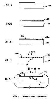
[PROCESS FOR PRODUCTION]
Fig.2 outlines a process for production of such a planar
waveguide. First, a substrate 10 made of a silica glass plate is
.
CA 02266682 1999-03-17
prepared (S11). Then, a metal film 12 is formed on the surface
of the substrate 10 (S12). This is carried out, for example, by
placing the glass substrate 10 in a vacuum chamber and depositing
a metal on the surface of the glass substrate 10. This metal to
be deposited may be, for example, aluminum. Methods other than
deposition may also be used to form the metal film 12.
Next, a determined portion of the metal film 12 is removed
by etching, thereby forming two electrodes 12a and 12b (S13). In
this example, a straight gap is formed between both electrodes 12a
and 12b and etching is carried out by means of photolithography,
etc. That is to say, a resist is formed by deposition over the
entire surface of the metal film 12, and then the resist is
irradiated with light through a mask pattern to expose only the
desired area of the resist.
Next, doping of GeO2(germanium oxide) is carried out using
the electrodes 12a and 12b as a mask (S14). By this doping of
germanium oxide the, core area 14, which operates as a waveguide
with a refractive index different from the surrounding areas,
is formed in the doped area. In such a manner as described above,
the core area can be accurately formed in the area between the
electrodes and ultraviolet excitation poling can be accurately
performed on the core area. The core area may, of course, be
easily be formed in any suitable shape, while the positions of
the electrodes will of necessity correspond to the core area.
When an element having an unrestricted waveguide is formed,
germanium oxide or the like are added to the whole of the glass
substrate 10, and its refractive index is adjusted. Doping step
S14 is therefore omitted. In this example, the gap is established
--
CA 02266682 1999-03-17
by approximately 10~m.
Asdescribedabove,whentheelectrodes12aand12bareformed,
irradiation with ultraviolet light is carried out in a state where
a determined high voltage is applied between the electrodes 12a
and12b, andtheultravioletexcitationpolingtreatment isapplied
to the core area 14 (S15).
That is to say, a voltage of about 1 kV is applied between
the electrodes 12a and 12b. An electric field of about 106V/cm is
nowappliedtothecorearea 14. Inthisstate, apulsedArFexcimer
laser (wavelength 193nm) is used to irradiate the core area 14
with ultraviolet light. The energy density, repetitive interval
of pulse and irradiation time of this laser are about 36mJ/cm2,
about 10pps (pulse /second) and about 10 to about 30 minutes,
respectively.
However, there is a danger of discharge in an area facing
to the gap between the electrodes 12a and 12b. It is, therefore,
preferabletocarryout theultraviolet excitationpoling invacuo.
In this way, discharge between the electrodes 12a and 12b can be
prevented and effective ultraviolet excitation poling can be
achieved.
In the manner described above, optical nonlinearity can be
given to the core area 14. That is to say, with the above
ultraviolet excitation poling treatment, a primary electrooptical
coefficient (r) ofapproximately 6pm/Vcanbe obtained in thecore
area. ThiS is a value comparable to that of LiNbO3 and the like,
and is sufficient for the formation of an optical functional
element.
The electrodes 12a and 12b which were used in order to apply
CA 02266682 1999-03-17
voltage at the time of ultraviolet excitation poling in the planar
waveguide remain on the substrateandcan beusedto apply adesired
electric field to the core area 14. It is thereafter a simple
process to impart and operate any combination of a variety of
functions.
While the ultraviolet excitation poling was applied to only
one place in the present illustrative example, it may also be
preferable that the electrodes 12a and 12b be independently
formed at preferable locations on the glass substrate 10, and
that an elemental region having optical nonlinearity be formed on
each place on the glass substrate 10.
[MODIFICATION]
It may also be preferable to configure the present invention
by forming alternate and periodic regions having optical
nonlinearity and usual regions on the core area 14, and to use
these as grating sections. That is to say, as shown in Fig.3, the
nonlinear regions 16a having a different refractive index and
secondarynonlinearityare formedonthecorearea14perpindicular
to the lengthwise direction at predetermined intervals and with
specified width to form the grating section 16 along with the usual
regions 16b. Therefore, light which is transmitted through the
corearea14initslengthwisedirectionisreflectedandinterfered
by the grating section 16.
Therefractiveindexofthenonlinearregion16acanbealtered
by controlling the voltage applied between the electrodes 12a and
12b. Thewavelengthofreflectedand interfered lightthenbecomes
different, and the wavelength of the light which intercepts the
CA 02266682 1999-03-17
transmission can then be controlled by applied voltage and this
modification can beutilized as a wavelength switchor a wavelength
selection element.
A planar waveguide as described above may be formed in such
a manner as will be describe below. That is to say, optical fibers
are irradiated with ultraviolet light laser through a phase mask
at the time of the aforementioned ultraviolet excitation poling.
One example of the structure of the phase mask is illustrated in
Fig. 4. As shown in Fig. 4, a plurality of grooves 22 are formed
on the surface of one side of the plate substrate 20. The grooves
22 are formed in parallel with each other and at predetermined
spacings. Accordingly, a predetermined diffraction phenomenon
occurswhen parallellight istransmittedthroughthegrooves,with
high and low intensities of the light being repeated at
predetermined spacings. That is to say, fringe patterns (zebra
patterns) are formed, in which light-irradiated regions and
non-light-irradiatedregionsareperiodicallyrepeated. Further,
desired places can be irradiated with desired ultraviolet light
byusinga pluralityofphasemasks. The substrate20Ofthe phase
maskmay,forexample,bemadeofsilicaglass(SiO2)whichtransmits
ultraviolet light.
Accordingly, the optical nonlinearity can be given only to
the places irradiated with ultraviolet light and such the planar
waveguide as shown in Fig.3 can be formed.
And, when a voltage, particularly negative voltage (several
hundred V, approximately) is applied to such a planar waveguide
in a state where light of various wavelengths isconducted thereto,
the wavelength intercepted by such a waveguide shifts. Therefore,
CA 02266682 1999-03-17
this waveguide may be utilized as a wavelength switch. With
respect to positive and negative of voltage, the electric field
opposite to poling electric field may be taken as positive.
As mentioned above, the transmission strength of light of
6 the specific wavelength decreases at the grating element because
Bragg reflection occurs in the grating and light of the Bragg
wavelength is reflected.
Further, theBraggwavelengthshifts whenavoltageisapplied
and the Bragg reflection increases or decreases according to the
applied voltage because the core area 14 at the region irradiated
with ultraviolet light comes to have the nonlinearity by the
ultraviolet excitation poling and the primary electrooptical
effect occurs and the effective reflective index of the waveguide
changes.
Variation in refractive index by the electrooptical effect
(AnEO) can represented by the following equation;
~nEO=-n3rE/2. In this equation, n is the refractive index of
the core area of fiber, r is the primary electrooptical effect
coefficient and E is electric field strength.
Bragg wavelength (A2) is then represented by
A2=Aneff wherein A is a pitch of the grating. And, in the
consideration on the basis of coupling of forward and backward
(reflection) guided light, the peak reflectance (R) isrepresented
by
R=tan h2 ( K L), and 3dB band width (A A ) is represented by
AA=A2 {~r2+ ( /cL) 2} ~-S/2n~,~f L
wherein~Kisthe couplingcoefficient offorward and backward
(reflection) guided light, and is represented by
11
CA 02266682 1999-03-17
~=~nC~n~ /A3 n~ff . Wherein L is length of the grating
element.
AlSo, n~ff iS effective refractive index of guided light at
the grating section, nc is the refractive index of cladding,~n is
the magnitude of change in the refractive index forming periodic
structure, and ~is overlapping integral in forward and backward
transmission modes.
Therefore, neff ~n and ~ change depending upon ~nEO.
The relationship between the variation in the effective
refractive index (~nEO) and the applied voltage was studied
experimentally from the relationship between the changes in the
voltage applied and the changes in the Bragg wavelength. As the
result, the effective refractive index (n~ff) has a determined
negative slope to the changes in the voltage applied and changes
linearly. Thatistosay,theeffectiverefractiveindexdecreases
depending upon an application of voltage and the Bragg wavelength
shifts to the side of short wavelength.
And, in such the planar waveguide as described above, the
changes in the Bragg wavelength (A A3) to electric field (lV/
~m) is approximately 0.01 nm.
As described above, there is a linear relationship between
the applied voltage and the effective refractive index and it is
understood that the Pockels effect (the primary electrooptical
effect) on the basis of the secondary optical nonlinearity is
obtained.
It is, therefore, possible to switch light of a specific
wavelength by shifting the Bragg wavelength by an application of
voltage to control the transmission and non-transmission of laser
CA 02266682 1999-03-17
light. Particularly, the planar waveguide of the present working
embodiment is made of glass. Therefore, the connection with
conventional optical fiber may be easily carried out. That is to
say, theconnection by adhesive, laser fusing, melt-connection and
the like can be easily carried out. Further, the transmittance
of light at the element may be sufficiently maintained and mode
mismatch is prevented .
Stillfurther, theBraggwavelength maybeshiftedinmultiple
stepsby successivelychanging voltage applied. Thereby, thismay
be also utilized as a wavelength selection element by controlling
the transmitted wavelength.
Furthermore, in the present embodiment, the spacings of the
grating may be easily controlled by the phase mask. Therefore,
the grating element having desired Bragg wavelength may be easily
obtained.
[ ANOTHER STRUCTURE ]
The planar waveguide of the present invention may be utilized
in a variety of functional elements. For example, it may be
preferable as shown in Fig. 5 to design a structure where the core
area 14 is once divided to two branches which rejoin each other,
and the electrodes 12a and 12b are placed respectively to the
branched portions so as to apply voltage.
With such a structure, it is possible to control the phases
of two branched two light rays by controlling the voltage applied
tothetwobranchedportions, andit isthereforepossibletoeffect
the attenuation of output light by shifting the phases of both 180
degree and optical strength modulation.
CA 02266682 1999-03-17
Arrangementofelectrodesisnotrestrictedtothearrangement
shown in Fig.5,and electrodes 12c and 12d may also be placed on
the core area 14 as shown in Fig.6. In this case, the electrodes
12cand 12dmay bepreferablyformed afterremovaloftheelectrodes
12a and 12b which have been used at the time of ultraviolet light
poling. With such the structure, modulation similar to that
described above may be effected.
According to the planar waveguide of the present invention,
portions having optical nonlinearity may be formed on any desired
area of the glass substrate 10. Therefore, various kinds of
optical functional elements and optical functional circuits may
be formed.
For example, a signal generator, an optical switch/coupler,
or the like for the two-way optical transmission system shown in
Fig.7 may be configured using the planar waveguide of the present
invention. Thatistosay,twoterminalslOOareshowninthesystem
illustrated in Fig.7 (there are a number of terminals 100 in
conventional systems). These terminals 100 are connected with
optical fiber 102 via a transducer 104. The transducer 104
controls the connection of desired optical fiber 102.
Each terminal 100 comprises a light source lOOa, a signal
generator lOOb, an optical switch/coupler, and a light receiving
element lOOd. The light source lOOa is a laser source generating
a specific light,andthesignalgeneratorlOObopticallymodulates
that light to include the information to be transmitted. The
optical switch/coupler lOOc transmits the optical signals
generated from the signal generator lOOb to the transmission
optical fiber 102 at the time of transmission and supplies the
CA 02266682 1999-03-17
optical signals generated from the transmission optical fiber 102
to the light receiving element lOOd at the time of receiving. The
light receiving element lOOd transduces input optical signals to
electric signals. The information transmitted may be demodulated
by modulating the electric signals obtained by the light receiving
element lOOd. An optical connector 106 connects the terminal 100
with the transmission optical fiber 102.
As described above, a transmission system making use of
opticalfibermaybemadeup,andtheplanarwaveguideofthepresent
inventionmaybepreferablyutilizedwiththesignalgeneratorlOOb,
the optical switch/coupler lOOc, or the like.
[INDUSTRIAL APPLICABILITY]
The present invention may be utilized for an optical
16 functional element such as an optical signal generator, an optical
switch/coupler, or any similar element in an optical fiber
transmission system.
.. . . . ..