Language selection

Search

Patent 2267496 Summary

Third-party information liability

Some of the information on this Web page has been provided by external sources. The Government of Canada is not responsible for the accuracy, reliability or currency of the information supplied by external sources. Users wishing to rely upon this information should consult directly with the source of the information. Content provided by external sources is not subject to official languages, privacy and accessibility requirements.

Claims and Abstract availability

Any discrepancies in the text and image of the Claims and Abstract are due to differing posting times. Text of the Claims and Abstract are posted:

  • At the time the application is open to public inspection;
  • At the time of issue of the patent (grant).
(12) Patent: (11) CA 2267496
(54) English Title: A FRACTIONAL-N DIVIDER USING A DELTA-SIGMA MODULATOR
(54) French Title: DIVISEUR N-FRACTIONNE EMPLOYANT UN MODULATEUR DELTA-SIGMA
Status: Expired and beyond the Period of Reversal
Bibliographic Data
(51) International Patent Classification (IPC):
  • H03M 03/02 (2006.01)
  • H03L 07/197 (2006.01)
  • H03M 07/36 (2006.01)
(72) Inventors :
  • RILEY, THOMAS A.D. (Canada)
(73) Owners :
  • PHILSAR ELECTRONICS INC.
  • SKYWORKS SOLUTIONS, INC.
(71) Applicants :
  • PHILSAR ELECTRONICS INC. (Canada)
  • SKYWORKS SOLUTIONS, INC. (United States of America)
(74) Agent: GOWLING WLG (CANADA) LLP
(74) Associate agent:
(45) Issued: 2003-03-11
(22) Filed Date: 1999-03-30
(41) Open to Public Inspection: 1999-09-30
Examination requested: 1999-06-14
Availability of licence: N/A
Dedicated to the Public: N/A
(25) Language of filing: English

Patent Cooperation Treaty (PCT): No

(30) Application Priority Data:
Application No. Country/Territory Date
2,233,831 (Canada) 1998-03-31

Abstracts

English Abstract


A delta-sigma modulator having a dead-zone quantizer and an error shaping
digital
filter clocked by a signal which is periodic at the frequency of the
reference. A dead-zone
quantizer provides quantization of a high resolution digital word to a low
resolution
digital word with three or a higher odd number of possible output levels and
with an
output of zero for an input near the centre of the normal input range. The
delta-sigma
modulator is used in a fractional-N divider. The fractional-N divider is used
in a
fractional-N frequency synthesizer.


Claims

Note: Claims are shown in the official language in which they were submitted.


What is claimed is:
1. A fractional-N divider for use in a fractional-N frequency synthesizer, the
fractional-N divider comprising:
a. a dead zone quantizer, the dead zone quantizer responding to a high
resolution digital word and the dead zone quantizer providing a first low
resolution digital word;
b. an error shaping filter, the error shaping filter responding to a fixed-
point
binary input signal, the first low resolution digital word and a clock signal
and the error shaping filter providing the high resolution digital word;
c. a first summer, the first summer responding to the first low resolution
digital word and a programmed base value and the first summer providing
a control signal; and
d. a programmable divider, the programmable divider responding to a
synthesizer output signal and the control signal and the programmable
divider providing a divided signal.
2. A fractional-N divider as recited in claim 1, further comprising:
a. a filter for contiguous tuning means, the filter responding to the first
low
resolution digital word and the clock signal and the filter providing a
filtered first low resolution digital word; and
b. wherein the summer is responding to the filtered first low resolution
digital word.
3. A fractional-N divider as recited in claim l, the fractional-N divider
further
comprising:
a. a residual error compensator, the residual error compensator responding
to the first low resolution digital word and the clock signal and the high
resolution digital word and the residual error compensator providing a
higher order, noise shaped first low resolution digital word.
-11-

4. A fractional-N divider as recited in claim 3 wherein the residual error
compensator
comprises:
a. a third summer, the third summer responding to the high resolution digital
word and the first low resolution digital word and the third summer
providing an error signal proportional to the difference between the high
resolution digital,word and the first low resolution digital word;
b. a delta-sigma modulator, the delta-sigma modulator responding to the
error signal and the clock signal and the delta-sigma modulator providing
a second low resolution digital word;
c. a fourth filter, the fourth filter responding to the second low resolution
digital word and the clock signal and the fourth filter providing a filtered
second low resolution digital word; and
d. a fourth summer, the fourth summer responding to the filtered second low
resolution digital word and the first low resolution digital word and the
fourth summer providing the higher order, noise shaped first low
resolution digital word.
5. A fractional-N divider as recited in claim 1, wherein the error shaping
filter
comprises:
a. a first filter, the first filter responding to the first low resolution
digital
word and the clock signal and the first filter providing a loop stabilizing
signal;
b. a second summer, the second summer responding to the fixed-point
binary input and the loop stabilizing signal and the second summer
providing a difference signal proportional to the difference between the
fixed-point binary input and the loop stabilizing signal; and
c. a second filter, the second filter responding to the difference signal and
the clock signal and the second filter providing the high resolution digital
word.
-12-

6. A fractional-N divider as recited in claim 5, wherein the second filter
provides a
Stabilizing-Zero transfer function.
7. A fractional-N divider as recited in claim 5, wherein the second filter
provides a
constant transfer function.
8. A fractional-N divider as recited in claim 5, wherein the first filter
comprises:
a. a first storage register, the first storage register responding to the
first low
resolution digital word and the clock signal and the first storage register
providing a first lookup table input signal;
b. a second storage register, the second storage register responding to the
first lookup table input signal and the clock signal and the second storage
register providing a second lookup table input signal; and
c. a lookup table, the lookup table responding to the first lookup table input
signal, the second lookup table signal and the fixed point binary input and
the lookup table providing a lookup table output signal.
9. A fractional-N divider as recited in claim 5, wherein the second filter is
an all pole
filter with poles at a frequency substantially equal to zero.
10. A fractional-N divider as recited in claim 5, wherein the second filter
has poles at
frequencies higher than zero.
11. A fractional-N divider as recited in claim 5, wherein the second filter
comprises:
a. a first digital adder, the first digital adder responding to the lookup
table
output signal, the fixed point binary input and a third register output
signal and the first digital adder providing a first digital adder output
signal;
b. a second digital adder, the second digital adder responding to the first
digital adder output signal and a fourth register output signal and the
second digital adder providing the high resolution digital word;
-13-

c. a third register, the third register responding to the clock signal and the
first digital adder output signal and the third register providing the third
register output signal; and
d. a fourth register, the fourth register responding to the clock and the
second digital adder output signal and the fourth register providing the
second register output signal.
12. A fractional-N divider as recited in claim 5,
a. wherein the first filter comprises:
a first storage register, the first storage register responding to the
first low resolution digital word and the clock signal and the first
storage register providing a first lookup table input signal;
ii. a second storage register, the second storage register responding
to the first lookup table input signal and the clock signal and the
second storage register providing a second lookup table input
signal; and
iii. a lookup table, the lookup table responding to the first lookup
table input signal, the second lookup table signal and the fixed
point binary input and the lookup table providing a lookup table
output signal; and
b. wherein the second filter comprises:
i. a first digital adder, the first digital adder responding to the
lookup table output signal, the fixed point binary input and a third
register output signal and the first digital adder providing a first
digital adder output signal;
ii. a second digital adder, the second digital adder responding to the
first digital adder output signal and a fourth register output signal
and the second digital adder providing the high resolution digital
word;
-14-

iii. a third register, the third register responding to the clock signal
and the first digital adder output signal and the third register
providing the third register output signal; and
iv. a fourth register, the fourth register responding to the clock and
the second digital adder output signal and the fourth register
providing the second register output signal.
13. A fractional-N divider for use in a fractional-N frequency synthesizer,
the
fractional-N divider comprising:
a. a dead zone quantizer, the dead zone quantizer responding to a high
resolution digital word and the dead zone quantizer providing a first low
resolution digital word;
b. an error shaping filter, the error shaping filter responding to a fixed-
point
binary input signal, the first low resolution digital word and a clock signal
and the error shaping filter providing the high resolution digital word,
wherein the error shaping filter comprises:
i. a first filter, the first filter responding to the first low resolution
digital word and the clock signal and the first filter providing a
loop stabilizing signal, wherein the first filter comprises:
(1) a first storage register, the first storage register responding
to the first low resolution digital word and the clock signal
and the first storage register providing a first lookup table
input signal;
(2) a second storage register, the second storage register
responding to the first lookup table input signal and the
clock signal and the second storage register providing a
second lookup table input signal; and
(3) a lookup table, the lookup table responding to the first
lookup table input signal, the second lookup table signal
and the fixed point binary input and the lookup table
providing a lookup table output signal;
-15-

ii. a second summer, the second summer responding to the fixed-point
binary input and the loop stabilizing signal and the second
summer providing a difference signal proportional to the
difference between the fixed-point binary input and the loop
stabilizing signal;
iii. a second filter, the second filter responding to the difference
signal and the clock signal and the second filter providing the high
resolution digital word, wherein the second filter comprises:
(1) a first digital adder, the first digital adder responding to
the lookup table output signal, the fixed point binary input
and a third register output signal and the first digital adder
providing a first digital adder output signal;
(2) a second digital adder, the second digital adder responding
to the first digital adder output signal and a fourth register
output signal and the second digital adder providing the
high resolution digital word;
(3) a third register, the third register responding to the clock
signal and the first digital adder output signal and the third
register providing the third register output signal; and
(4) a fourth register, the fourth register responding to the
clock and the second digital adder output signal and the
fourth register providing the second register output
signal;
c. a programmable divider, the programmable divider responding to a
synthesizer output signal and the control signal and the programmable
divider providing a divided signal;
d. a filter for contiguous tuning means, the filter responding to the first
low
resolution digital word and the clock signal and the filter providing a
filtered first low resolution digital word;
-16-

e. a first summer, the first summer responding to the filtered first low
resolution digital word and a programmed base value and the first
summer providing a control signal; and
f. a residual error compensator, the residual error compensator responding
to the first low resolution digital word and the high resolution digital
word and the clock signal and the residual error compensator providing
a higher order, noise shaped first low resolution digital word, wherein the
residual error compensator comprises:
i. a third summer, the third summer responding to the high
resolution digital word and the first low resolution digital word
and the third summer providing an error signal proportional to the
difference between the high resolution digital word and the first
low resolution digital word;
ii. a delta-sigma modulator, the delta-sigma modulator responding
to the error signal and the clock signal and the delta-sigma
modulator providing a second low resolution digital word;
iii. a fourth filter, the fourth filter responding to the second low
resolution digital word and the clock signal and the fourth filter
providing a filtered second low resolution digital word; and
iv. a fourth summer, the fourth summer responding to the filtered
second low resolution digital word and the first low resolution
digital word and the fourth summer providing the higher order,
noise shaped first low resolution digital word.
14. A delta-sigma modulator for use in a fractional-N frequency divider, the
delta-
sigma modulator comprising
a. a dead zone quantizer, the dead zone quantizer responding to a high
resolution digital word and the dead zone quantizer providing a first low
resolution digital word; and
-17-

b. an error shaping filter, the error shaping filter responding to a fixed-
point
binary input signal, the first low resolution digital word and a clock signal
and the error shaping filter providing the high resolution digital word.
15. A delta-sigma modulator as recited in claim 14, wherein the error shaping
filter
comprises:
a. a first filter, the first filter responding to the first low resolution
digital
word and the clock signal and the first filter providing a loop stabilizing
signal;
b. a second summer, the second summer responding to the fixed-point
binary input and the loop stabilizing signal and the second summer
providing a difference signal proportional to the difference between the
fixed-point binary input and the loop stabilizing signal; and
c. a second filter, the second filter responding to the difference signal and
the clock signal and the second filter providing the high resolution digital
word.
16. A delta-sigma modulator as recited in claim 15, wherein the second filter
provides
a Stabilizing-Zero transfer function.
17. A delta-sigma modulator as recited in claim 15, wherein the second filter
provides
a constant transfer function.
18. A delta-sigma modulator as recited in claim 15, wherein the first filter
comprises:
a. a first storage register, the first storage register responding to the
first low
resolution digital word and the clock signal and the first storage register
providing a first lookup table input signal;
b. a second storage register, the second storage register responding to the
first lookup table input signal and the clock signal and the second storage
register providing a second lookup table input signal; and
-18-

c. a lookup table, the lookup table responding to the first lookup table input
signal, the second lookup table signal and the fixed point binary input and
the lookup table providing a lookup table output signal.
19. A delta-sigma modulator as recited in claim 15, wherein the second filter
is an all
pole filter with poles at a frequency substantially equal to zero.
20. A delta-sigma modulator as recited in claim 15, wherein the second filter
has poles
at frequencies higher than zero.
21. A delta-sigma modulator as recited in claim 15, wherein the second filter
comprises:
a. a first digital adder, the first digital adder responding to the lookup
table
output signal, the fixed point binary input and a third register output
signal and the first digital adder providing a first digital adder output
signal;
b. a second digital adder, the second digital adder responding to the first
digital adder output signal and a fourth register output signal and the
second digital adder providing the high resolution digital word;
c. a third register, the third register responding to the clock signal and the
first digital adder output signal and the third register providing the third
register output signal; and
d. a fourth register, the fourth register responding to the clock and the
second digital adder output signal and the fourth register providing the
second register output signal.
22. A delta-sigma modulator as recited in claim 15, wherein:
a. a first storage register, the first storage register responding to the
first low
resolution digital word and the clock signal and the first storage register
providing a first lookup table input signal;
-19-

b. a second storage register, the second storage register responding to the
first lookup table input signal and the clock signal and the second storage
register providing a second lookup table input signal;
c. a lookup table, the lookup table responding to the first lookup table input
signal, the second lookup table signal and the fixed point binary input and
the lookup table providing a lookup table output signal;
d. a first digital adder, the first digital adder responding to the lookup
table
output signal, the fixed point binary input and a third register output
signal and the first digital adder providing a first digital adder output
signal;
e. a second digital adder, the second digital adder responding to the first
digital adder output signal and a fourth register output signal and the
second digital adder providing the high resolution digital word;
f. a third register, the third register responding to the clock signal and the
first digital adder output signal and the third register providing the third
register output signal; and
g. a fourth register, the fourth register responding to the clock and the
second digital adder output signal and the fourth register providing the
second register output signal.
-20-

Description

Note: Descriptions are shown in the official language in which they were submitted.


CA 02267496 1999-03-30
A Fractional-N Divider Using a Delta-Sigma Modulator
Field of the Invention
This invention relates generally to fractional-N dividers, and more
specifically to
delta-sigma modulators used in fractional-N dividers.
Background
Fractional-N single-loop phase locked loop (PLL) synthesizers are often used
for
generating one frequency from a range of predetermined desirable frequencies.
Typically
this technique is performed for the purpose of transmitting or receiving a
radio signal
over one frequency channel of many possible allocations.
The structure of many fractional-N single-loop PLL synthesizers is shown in
Figure 1. A voltage controlled oscillator (VCO) 10 provides an output signal
12, f,
oscillating with a frequency responsive to a control signal 14, s2. A
fractional-N divider
16 provides a divided signal 18, f~,, such that the frequency ofd', is the
frequency of f
divided by some desired division ratio, N. A phase detector 20 provides a
signal 22, s 1,
such that the signal 22, s 1, is proportional to the phase or frequency
difference between
f~, and a reference frequency signal 24, ~. A loop filter 26, F(s), provides
the control
signal 14, s2 so that the overall loop is a stable phase locked loop.
The output frequency 12, f" of such a synthesizer depends on the reference
frequency 24, f , and the desired division ratio, N. Specifically, f,; = Nf .
Often a component of the fractional-N divider 20 is a delta-sigma modulator
26.
In delta-sigma controlled synthesizers, the value of N can take on fractional
values.
Typically, this is provided by a programable divider 28, responsive to some
programmed
base value 30, n, and a first low resolution digital word 32, b;, of the delta-
sigma
modulator 26. A first summer 34 provides a control signal 36, c, such that the
programmable divider 28 divides by predetermined ratios n, n+1, n+2, ... n+k;
where k
is some predetermined integer which depends on the particular delta-sigma
modulator 26
used. Various other means, known to those versed in the art, may be provided
such that
the delta-sigma modulator 26 selects one of the predetermined division ratios
for each
cycle of the programable divider 28.
-1-

CA 02267496 1999-03-30
Thus, if the delta-sigma modulator 26 has a fixed-point binary input 38, buv~,
first
low resolution digital word, 32, b;, for each cycle of the programmable
divider 28, there
is some time average value for this such that b; = buv~ + ~7 where l~v~ is the
desired,
fractional, average output and Q; is the quantization error for each cycle of
the
programmable divider 28. Since b~ry~ is a long term average of many integers,
it can have
a fractional value and fractional-N division may be achieved.
In the short term, there is often an non-zero quantization error. A delta-
sigma
modulator 26 is defined herein by the ability to shape the spectral density of
this
quantization error. The noise shaping provided by the delta-sigma modulator 26
is such
that the quantization error is reduced at and near to a frequency
substantially equal to
zero, the reference frequency 24, f , and all multiples the reference
frequency 24, f .
This error shaping allows the quantization error to be substantially removed
by the
low pass filtering of the closed-loop PLL.
Although all delta-sigma modulators have the same functional definition, some
delta-sigma modulators perform better than others in the ability to randomize
and noise
shape the quantization error. Some specific limitations are as follows.
With an input signal with a frequency substantially equal to zero, any digital
delta-
sigma modulator becomes a finite state machine. A delta-sigma modulator which
has a
longer sequence length, which in turn produces more spurious signals, will
generally
have less power in each individual spurious signal. The power in each of these
spurious
signals can presently limit the performance of a delta-sigma modulator based
fractional-N
synthesizer, especially when it is desirable to reduce the number of bits in
the delta-sigma
modulator. This creates difficulty in designing low power synthesizers with
low spurious
signals.
Another factor which limits the performance of delta-sigma modulator based
fractional-N synthesizers is high frequency spurious signals outside the loop
bandwidth
of the PLL synthesiser. When these spurious signals are substantially larger
than those
produced by sequence length limits, any nonlinearity substantially equivalent
to a phase
detector nonlinearity can mix these spurious signals to new frequencies within
the
bandwidth of the PLL. These spurious signals often can not be filtered out by
the loop
filter.
-2-

CA 02267496 1999-03-30
Further, different delta-sigma modulators involve different amounts of digital
hardware. In an large scale integration implementation, this hardware consumes
silicon
area and power, both of which are disadvantageous for low cost portable
equipment.
For the foregoing reasons, there is a need to provide a fractional-N divider
which
uses a delta-sigma modulator with reduced spurious signals.
Summary
The present invention is directed to a fractional-N divider which uses a delta-
sigma
modulator to provide reduced spurious signals.
The present invention provides a delta-sigma modulator for use in a fractional-
N
frequency divider, the delta-sigma modulator comprising a dead zone quantizer
and an
error shaping filter. The dead zone quantizer responds to a high resolution
digital word.
The dead zone quantizer provids a first low resolution digital word. The error
shaping
filter responds to a fixed-point binary input signal, the first low resolution
digital word
and a clock signal. The error shaping filter provides the high resolution
digital word.
An advantage of the present invention is reduced spurious signals, and thus
improved fractional-N divider performance.
Brief Description of the Drawings
These and other features, aspects, and advantages of the present invention
will
become more apparent from the following description, appended claims, and
accompanying drawings where:
Figure 1 illustrates in block diagram form, the general architecture of a
single-loop delta-
sigma fractional-N synthesizer;
Figure 2 illustrates in block diagram form, an embodiment of a delta-sigma
modulator
in accordance with the present invention;
Figure 3 illustrates a single loop feedback delta-sigma modulator with an
error shaping
filter according to a further embodiment of the invention;
Figure 4 illustrates a single loop feedback second order delta-sigma modulator
according
to an optional aspect of the invention;
-3-

CA 02267496 1999-03-30
Figure 5 illustrates a fractional-N divider with contiguous tuning across
integer-N
boundaries according to an optional aspect of the invention;
Figure 6 illustrates a higher order delta-sigma modulator according to an
optional aspect
of the invention; and
Figure 7 illustrates, by example, the input and output values for a dead zone
quantizer
according to an embodiment of the invention.
Detailed Description
By way of overview, this description is presented as follows. First, the
structure of
the fractional-N divider is described. Second, the operation of the fractional-
N divider is
described. Third, the advantages of the fractional-N divider are described.
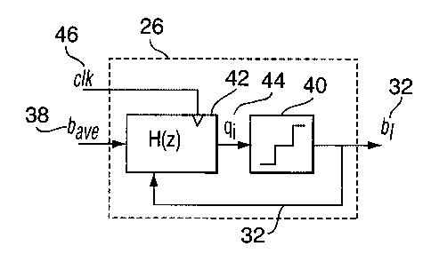
Figure 1 illustrates a fractional-N divider 16 for use in a fractional-N
frequency
synthesizer. Figure 2 illustrates the structure of the delta-sigma modulator
26 of Figure 1
in accordance with the invention. Thus, the fractional-N divider 16 comprises
a dead zone
quantizer 40, an error shaping filter 42, a first summer 34 and a programmable
divider
28. The dead zone quantizer 40 responds to a high resolution digital word 44.
The dead
zone quantizer 40 provides a first low resolution digital word 32. The error
shaping filter
42 responds to a fixed-point binary input signal 38, the first low resolution
digital word
32 and a clock signal 46. The error shaping filter 42 provides the high
resolution digital
word 44. Tthe first summer 34 responds to the first low resolution digital
word 32 and
a programmed base value 30 . The first summer 34 provides a control signal 36.
The
programmable divider 28 responds to a synthesizer output signal 12 and the
control
signal 36. The programmable divider 28 provides a divided signal 18.
Turning now to Figure 3, an optional embodiment of the error shaping filter 42
is
shown. The error shaping filter 42 comprises a first filter 48, a second
summer 50 and a
second filter 52. The first filter responds to the first low resolution
digital word 32 and
a clock signal 46. The first filter 48 provides a loop stabilizing signal 54.
The second
summer 50 responds to the fixed-point binary input 38 and the loop stabilizing
signal 54.
The second summer 50 provides a difference signal 56 proportional to the
difference
between the fixed-point binary input 38 and the loop stabilizing signal 54.
The second
-4-

CA 02267496 1999-03-30
filter 52 responds to the difference signal 56 and a clock signal 46. The
second filter 52
provides the first low resolution digital word 32.
In Figure 4 an optional embodiment of the error shaping filter 42 is shown.
The first
filter 48 of Figure 3 comprises a first storage register 58, a second storage
register 60 and
a lookup table 62. The first storage register 58 responds to the first low
resolution digital
word 32 and the clock signal 46. The first storage register 58 provides a
first lookup table
input signal 64. The second storage register 60 responds to the first lookup
table input
signal 64 and the clock signal 46. The second storage register 60 provides a
second
lookup table input signal 66. The lookup table 62 responds to the first lookup
table input
signal 64, the second lookup table signal 66 and the most significant bit of
the fixed point
binary input 38. The lookup table 62 provides a lookup table output signal 68.
Furthermore, the second filter 52 of Figure 3 comprises a first digital adder
70, a second
digital adder 72, a third register 74 and a fourth register 76. The first
digital adder 70
responds to the lookup table output signal 68, the fixed point binary input 38
and a third
register output signal 78. The first digital adder 70 provides a first digital
adder output
signal 80. The second digital adder 72 responds to the first digital adder
output signal 80
and a fourth register output signal 82. The second digital adder 72 provides
the high
resolution digital word 44. The third register 74 responds to the clock signal
46 and the
first digital adder output signal 80. The third register 74 provides the third
register output
signal 78. The fourth register 76 responds to the clock 46 and the high
resolution digital
word 44. The fourth register 76 provides the fourth register output signal 82.
In the optional embodiment of the invention shown in Figure 5, the fractional-
N
divider 16 further comprises a filter 84 for contiguous tuning means. The
filter 84
responds to the first low resolution digital word 32 and the clock signal 46.
The filter 84
provides a filtered first low resolution digital word 86. Also, in this
embodiment, the first
summer 34 responds to the filtered first low resolution digital word 86.
In the optional embodiment of the invention shown in Figure 6, the fractional-
N
divider 16 further comprises a residual error compensator 88. The residual
error
compensator 88 responds to the first low resolution digital word 32, the clock
signal 46
and the high resolution digital word 44. The residual error compensator 88
provides a
higher order, noise shaped first low resolution digital word 90.
-5-

CA 02267496 1999-03-30
In Figure 6, the residual error compensator 88 comprises a third summer 92, a
second delta-sigma modulator 94, a fourth filter 96 and a fourth summer 98.
The third
summer 92 responds to the high resolution digital word 44 and the first low
resolution
digital word 32. Third summer 92 provides an error signal 100 proportional to
the
difference between the high resolution digital word 44 and the first low
resolution digital
word 32. The second delta-sigma modulator 94 responds to the error signal 100
and the
clock signal 46. The second delta-sigma modulator 94 provides a second low
resolution
digital word 102. The fourth filter 96 responds to the second low resolution
digital word
102 and the clock signal 46. The fourth filter 96 provides a filtered second
low resolution
digital word 104. The fourth summer 98 responds to the filtered second low
resolution
digital word 104 and the first low resolution digital word 32. The fourth
summer 98
provides the higher order, noise shaped first low resolution digital word 90.
The operation of the invention is now described. Figure 2 illustrates the
delta-sigma
modulator 16 comprising the dead-zone quantizer 40 and the error shaping
filter 42. The
error shaping filter 42 is clocked by the clock signal 46, clk, which is
periodic at the
frequency of the reference 24. The dead-zone quantizer 40 provides
quantization of the
high resolution digital word 44, q;, to the low resolution digital word 32,
b;, with 3 or a
higher odd number of possible output levels and with an output of 0 for an
input near the
centre of the normal input range. This provides different quantization error
than a dicer
or single bit quantizer.
Figure 7 illustrates by example, the input and output values for a quantizer
40 with
two's compliment binary encoding of the numerical values. In this example the
output
values are -1,0 and +1. Other numbers of output levels are also possible. Bit
positions
marked with an x in Figure 7 are don't cares and hence the output value is a
logic
function of the three most significant bits of the input value. Extra most
significant bits
may be added as necessary by sign extending the quantizer 40 input value to
provide
sufficient dynamic range for the variations in signal magnitude in each of the
accumulators, or resonators, prior to the quantizer 40.
The error shaping digital filter 42 clocked at the frequency of the reference
24, f ,
provides spectral shaping of the quantization error introduced by the dead-
zone quantizer
-6-

CA 02267496 1999-03-30
40 and a stable delta-sigma modulator. Many stable delta-sigma modulators have
been
presented in the literature and are known to those versed in the art.
Delta-Sigma Data Converters: Theory Design and Simulation (Norsworthy et al.)
is
included herein by reference. The error shaping filter 42 is responsive to
both the fixed
point binary input signal 38 buv~ and the quantizer output value, the first
low resolution
digital word 32, b; such that the overall delta-sigma modulator provides a low
pass or
substantially all pass filter from ba~e to b;, and a notch filter to reduce
the spectral density
of the quantization error at a frequency substantially equal to zero and
multiples of the
clock frequency.
As with single bit quantizers or multibit quantizers, described in the prior
art, the
error shaping filter 42 must provide negative feedback and a stable feedback
loop to
control the quantization error. The feedback is accomplished by the input of
the first low
resolution digital word 32 to the error shaping filter 42.
To further clarify without reducing generality, one particular example
illustrated in
Figure 3 teaches that, according to an optional aspect of the invention, the
first filter 48
G 1 (z) provides a Stabilizing-Zero transfer function. The Stabilizing-Zero
transfer
function is K[ 1 -( 1 -z -' )P] . In the forgoing equation P is the order of
the delta-sigma
modulator 16 and the number of accumulators in the feed-forward path, and K is
2 raised
to the power of an integer number.
Alternatively, the transfer function of the first filter 48 G 1 (z) may be a
constant,
with the stabilizing zeros included in the second filter 52.
The second filter 52 G2(z), with substantial gain at or near a frequency
substantially
equal to zero and multiples of the reference frequency 24, provides the
quantizer input
value for the dead-zone quantizer 40.
Typically, the second filter 52 G2(z) is an all pole filter with poles at a
frequency
substantially equal to zero. In this case, the second filter 52 is provided by
two or more
accumulators. To position quantization error noise notches at other
frequencies, the
second filter 52 could include a series of resonators and/or accumulators to
move the
poles of G2(z) to frequencies higher than zero.
Another embodiment the invention provides the first filter 48 of this type,
with
coefficients that are all even powers of two.

CA 02267496 1999-03-30
The error shaping filter 42 of Figure 4 teaches by examples an optional aspect
of
the invention which is the employment of the error shaping filter 42 which has
a regular
layout and minimal hardware when implemented in an large scale integration
circuit. The
first storage register 58 stores the previous value of the quantizer output,
the first low
resolution digital word 32 b;, and provides the delayed version of the output
64, b;'. The
second storage register 60 stores the delayed version of the output 64, b;',
and provides
a twice delayed version of the quantizer output 66, b; ". The lookup table 62
stores and
provides precomputed differences 68, e;, selected by the first filter 48
function G 1 (z) and
the fixed-point binary input 38 b~,~. A first accumulator comprises a digital
adder 70 and
register 74 and provides an accumulated output 80, a;. A second accumulator
comprises
a digital adder 72 and register 76 and provides the input, the high resolution
digital word
44 to the dead-zone quantizer 40. The accumulators are also known as
integrators.
The transfer function is of the error shaping filter 42 may be -[(1-z')2-1]K
where
K is as previously defined and z' is the delay operator.
It will be clear to those versed in the art of digital electronics, that the
resolution of
the delta-sigma modulator can be increased by one or more bits by increasing
the bus
widths of the input and the accumulators in the path of the second filter 52.
Similarly, the
resolution of the delta-sigma modulator can be decreased by one or more bits
by
decreasing the bus widths of the input and the accumulators in the path of the
second
filter 52.
It will be clear to those versed in the art of digital electronics, that other
forms of
digital logic could replace the lookup table with equivalent functionality. In
general, the
minimal hardware and regular layout are provided by the single loop feed-back
and
power of two scaling factors in the feed-back filter.
For higher order delta-sigma modulators, the two integrators of Figure 4 may
be
generalized to two or more integrators and the two delays of the output, the
first low
resolution signal 32 b;, can be generalized to two or more delays.
In some cases, it may be desirable to use the output 64 b;' rather than the
first low
resolution digital word 32 b; as the delta-sigma modulator 16 output. The
output 64 b;'
provides a delayed and resynchronized output. b;' 64 can be regarded as
equivalent to the
first low resolution digital word 32 b; once this delay is taken into account.
_g_

CA 02267496 1999-03-30
The previously described embodiments of the present invention have many
advantages, including the following. The embodiments described above reduce
the
performance degrading effects of spurious signals within the loop bandwidth of
the
fractional-N frequency sysnthesizer. This reduction is accomplished by one of
two
advantages, or both. Firstly, spurious signals occurring within the loop
bandwidth are
reduced. Second, spurious signals occurring outside the loop bandwidth are
reduced, so
that when these out of band spurious signals are mixed into the loop bandwidth
by
nonlinearities, the resulting inband spurious signals are reduced.
A further advantage the embodiment shown in Figure 4 above is an error shaping
filter with reduced hardware and regular layout when implemented in a large
scale
integration circuit.
Further examples and embodiments of the invention are now outlined. Figure 5
teaches by example an apparatus for obtaining contiguous tuning without having
excessively large values in the accumulators. A filter 82, responsive to the
delta-sigma
output, the first low resolution digital word 32 b;, provides an output
signal, the filtered
first low resolution digital word 86 c', which controls the divide ratio of
the
programmable divider 28. The filter 82 provides a fixed gain at a frequency
substantially
equal to zero, K~"~.n greater than 1. This gain is provided such that the
fixed point binary
input 38 bQV~., which varies over a range from ba~~ =a to hv~. =a + 1/I~,~, ,
and provided a
corresponding filtered low resolution digital word 86 c ', which varies over a
range from
aK,;,,~, to aK~,,~r+ 1.
Optionally, changing the programmable base value 30, n, provides a frequency
synthesizer tuning range which can be contiguously tuned across integer-n
boundaries.
In the example of Figure 5, the filter 82 adds the present output of the delta-
sigma
modulator 16 to the previous output of the delta-sigma modulator 16 provides a
gain of
two at a frequency substantially equal to zero. As a result, varying the
component at a
frequency substantially equal to zero of the first low resolution digital word
32 b; over
a range from -0.25 to +0.25 causes the component at a frequency substantially
equal to
zero of the filtered first low resolution signal 86 to vary over a range from -
0.5 to +0.5.
Figure 6 illustrates an apparatus for compensating residual error of the dead-
zone
quantizer 40 which is not completely removed by the error shaping filter 42.
The third
-9-

CA 02267496 1999-03-30
summer 92 detects the residual error and provides an error signal 100, r,
corresponding
to the error introduced by the dead-zone quantizer 40. The delta-sigma
modulator 94
responds to the error signal 100 r, and the clock signal 46 clk. The delta-
sigma modulator
94 provides the second low resolution digital word 102 b2, such that b2 102
represents
the error signal 100, r. The quantization error introduced by the delta-sigma
modulator
16 is reduced at or near a frequency substantially equal to zero and all
multiples of the
frequency of the clock signal 46 clk. The fourth filter responsive to the
second low
resolution digital word 102 and clock signal 46, clk, providing signal
filtered second low
resolution signal 104 b3, such that the transfer function provided for b3 from
b2 is ( 1-z
')2. The fourth summer 98 responds to filtered second low resolution signal
104 b3, and
the first low resolution digital word 32 b;.
Although the present invention has been described in considerable detail with
reference to certain preferred versions thereof, other versions are possible.
Therefore, the
spin and scope of the appended claims should not be limited to the description
of the
preferred versions contained herein.
-10-

Representative Drawing
A single figure which represents the drawing illustrating the invention.
Administrative Status

2024-08-01:As part of the Next Generation Patents (NGP) transition, the Canadian Patents Database (CPD) now contains a more detailed Event History, which replicates the Event Log of our new back-office solution.

Please note that "Inactive:" events refers to events no longer in use in our new back-office solution.

For a clearer understanding of the status of the application/patent presented on this page, the site Disclaimer , as well as the definitions for Patent , Event History , Maintenance Fee  and Payment History  should be consulted.

Event History

Description Date
Time Limit for Reversal Expired 2008-03-31
Letter Sent 2007-03-30
Inactive: IPC from MCD 2006-03-12
Letter Sent 2003-08-08
Grant by Issuance 2003-03-11
Inactive: Cover page published 2003-03-10
Inactive: Office letter 2002-12-18
Pre-grant 2002-12-11
Inactive: Final fee received 2002-12-11
Notice of Allowance is Issued 2002-06-12
Letter Sent 2002-06-12
Notice of Allowance is Issued 2002-06-12
Inactive: Approved for allowance (AFA) 2002-05-31
Inactive: Entity size changed 2002-03-14
Letter Sent 2000-06-28
Inactive: Multiple transfers 2000-05-23
Application Published (Open to Public Inspection) 1999-09-30
Inactive: Cover page published 1999-09-29
Letter Sent 1999-08-23
Inactive: Single transfer 1999-07-27
Inactive: Correspondence - Formalities 1999-06-30
Inactive: Correspondence - Transfer 1999-06-30
Letter Sent 1999-06-30
Request for Examination Received 1999-06-14
Request for Examination Requirements Determined Compliant 1999-06-14
All Requirements for Examination Determined Compliant 1999-06-14
Inactive: First IPC assigned 1999-05-20
Inactive: Filing certificate - No RFE (English) 1999-05-05
Application Received - Regular National 1999-05-03

Abandonment History

There is no abandonment history.

Maintenance Fee

The last payment was received on 2002-03-07

Note : If the full payment has not been received on or before the date indicated, a further fee may be required which may be one of the following

  • the reinstatement fee;
  • the late payment fee; or
  • additional fee to reverse deemed expiry.

Patent fees are adjusted on the 1st of January every year. The amounts above are the current amounts if received by December 31 of the current year.
Please refer to the CIPO Patent Fees web page to see all current fee amounts.

Owners on Record

Note: Records showing the ownership history in alphabetical order.

Current Owners on Record
PHILSAR ELECTRONICS INC.
SKYWORKS SOLUTIONS, INC.
Past Owners on Record
THOMAS A.D. RILEY
Past Owners that do not appear in the "Owners on Record" listing will appear in other documentation within the application.
Documents

To view selected files, please enter reCAPTCHA code :


To view images, click a link in the Document Description column. To download the documents, select one or more checkboxes in the first column and then click the "Download Selected in PDF format (Zip Archive)" or the "Download Selected as Single PDF" button.

List of published and non-published patent-specific documents on the CPD .

If you have any difficulty accessing content, you can call the Client Service Centre at 1-866-997-1936 or send them an e-mail at CIPO Client Service Centre.


Document
Description 
Date
(yyyy-mm-dd) 
Number of pages   Size of Image (KB) 
Representative drawing 2003-02-03 1 5
Claims 1999-03-29 10 401
Description 1999-03-29 10 545
Abstract 1999-03-29 1 15
Drawings 1999-03-29 4 69
Drawings 1999-06-29 4 71
Representative drawing 1999-09-21 1 4
Acknowledgement of Request for Examination 1999-06-29 1 179
Filing Certificate (English) 1999-05-04 1 165
Courtesy - Certificate of registration (related document(s)) 1999-08-22 1 139
Reminder of maintenance fee due 2000-12-03 1 112
Commissioner's Notice - Application Found Allowable 2002-06-11 1 165
Courtesy - Certificate of registration (related document(s)) 2003-08-07 1 107
Courtesy - Certificate of registration (related document(s)) 2003-08-07 1 106
Courtesy - Certificate of registration (related document(s)) 2003-08-07 1 107
Maintenance Fee Notice 2007-05-13 1 172
Correspondence 2002-12-18 1 18
Correspondence 2002-12-10 1 30
Correspondence 2000-06-27 1 23
Correspondence 1999-05-10 1 35
Correspondence 1999-06-29 5 99