Note: Descriptions are shown in the official language in which they were submitted.
CA 02267679 2003-12-22
P54818PCT
NTSC CO-CHANNEL INTERFERENCE DETECTORS RESPONSIVE TO
RECEIVED Q-CHANNEL SIGNALS IN DIGITAL TV SIGNAL RECEIVERS
The present invention relates to digital television systems, and more
particularly, to circuits employed in the digital television receiver for
determining
whether or not there is co-channel interference from NTSC analog television
signals.
BACKGROUND OF THE INVENTION
A Digital Television Standard published 16 September 1995 by the Advanced
Television Subcommittee (ATSC) specifies vestigial sideband (VSB) signals for
transmitting digital television (DTV) signals in 6-MHz-bandwidth television
channels
such as those currently used in over-the-air broadcasting of National
Television
Subcommittee (NTSC) analog television signals within the United States. The
VSB
DTV signal is designed so its spectrum is likely to interleave with the
spectrum of a
co-channel interfering NTSC analog TV signal. This is done by positioning the
pilot,
carrier and the principal amplitude-modulation sideband frequencies of the DTV
1 S signal at odd multiples of one-quarter the horizontal scan line rate of
the NTSC analog
TV signal that fall between the even multiples of one-quarter the horizontal
scan line
rate of the NTSC analog TV signal, at which even multiples most of the energy
of the
luminance and chrominance components of awco-channel interfering NTSC analog
TV
signal will fall. The video carrier of an NTSC analog TV signal is offset 1.25
MHz
from the lower lizn:it frequency of the television channel. The carrier of the
DTV
signal is offset from such video carrier by 59.75 times the horizontal scan
line rate of
the NTSC analog TV signal, to place the carrier of the DTV signal about
309;877.6
kHz from the lower limit frequency of the television channel. Accordingly, the
carrier
of the DTV signal is about 2,690122.4 Hz from the middle frequency of the
television
channel.
The exact symbol rate in the Digital Television Standard is (684/286) times
the 4.5 MHz sound carrier offset from video carrier in an NTSC analog TV sib
al.
The number of symbols per horizontal scan line in an N,,TSC analog TV signal
is 684,
and 286 is the factor by which horizontal scan line rate in an NTSC analog TV
signal
CA 02267679 2003-12-22
n
b C
~ v:.
P54818PCT ,
is multiplied to obtain the 4:5 MHz sound carrier offset from video carrier in
an
NTSC analog TV signal. The symbol rate is I 0.762238 rnegasymbols per second,
which can be contained in a VSB signal extending 5.3811 I9 MHz from DTV signal
carzier. That is, the VSB signal can be limited to a band extending 5.690997
MHz
S from the lower limit frequency of the television channel.
F
The ATSC standard for digital HDTV signal terrestrial broadcasting in the
United States of America is capable of transmitting either of two high-
definition
television (HDTV) formats with I6:9 aspect ratio. One HDTV display format uses
1920 samples per scan line and 1080 active horizontal scan lines per 30 Hz
frame with
IO 2:1 field interlace. The other HDTV display format use's 1280 luminance
samples per
scan line and 720 progressively scanned scan lines of television image per 60
Hz
frame. The ATSC standard also accommodates the transmission of DTV display
formats other.than HDTV display formats, such as the parallel transmission of
four
television signals having normal definition in comparison to an NTSC analog
15 television signal.
DTV transmitted by vestigial-sideband (VSB) amplitude modulation (A:M)
during terrestrial.broadcasting in the United States of America comprises a
succession
of consecutive-in-time data fields each containing 313 consecutive-in-time
data
segments. The data fields may be considered to be consecutively numbered
20 modulo-2, with each odd-numbered data field and the succeeding even-
numbered data
field forming a data frame. The frame rate is 20.66 frames per second. Each
data
segment is of 77.3 microseconds duration. So, with the symbol rate being 10.76
MHz
there axe 832 syrntiols per data segment. Each segment of data begins with a
line
synchronization code group of four symbols having successive values of+S, -S, -
S
25 and +S. The value +S is one level below the maximum positive data
excursion, and
the value -S is one level above the maximum negative data excursion. The
initial line
of each data field includes a field synchronization code group that codes a
training
signal for channel-equalization and multipath suppression procedures. The
training
signal is a 511-sample pseudo-noise sequence (or "PN-sequence") followed by
three
30 63-sample PN sequences. The middle ones of the 63-sample PN sequences in
the
2
CA 02267679 2003-12-22
r t;
..
P54818PCT
field synchronization codes are transmitted in accordance with a first logic
convention
in the first line of each odd-numbered. data field and in accordance with a
second logic
convention in the first line of each even-numbered data field, the first and
second
logic conventions being one's complementary respective to each other.
The data within data lines are trellis coded using twelve interleaved trellis
codes, each a 2/3 rate trellis code with one uncoded bit. The interleaved
trellis codes
are subjected to Reed-Solomon forward error-correction coding, which provides
for
correction of burst errors arising from noise sources such as a nearby
unshielded
automobile ignition system. The Reed-Solomon coding results are transmitted as
8-level (3 bits/symbol) one-dimensional-constellation symbol coding for over-
the-air
transmission, which transmissions are made without symbol precoding separate
from
the trellis coding procedure. The Reed-Solomon coding results are transmitted
as
16-level (4 bits/symbol) one-dimensional-constellation symbol coding for
cablecast,
which transmissions are made without precoding. The VSB signals have their
natural
carrier wave, which would vary in amplitude depending on the percentage of
modulation, suppressed.
The natural carrier wave is replaced by a pilot carrier wave of fixed
amplitude,
which amplitude corresponds to a prescribed percentage of modulation: This
pilot
carrier wave of fixed amplitude is generated by introducing a direct component
shift
into the modulating voltage applied to the balanced modulator generating the
amplitude-modulation sidebands that are supplied to the filter supplying the
VSB
signal as its response. If the eight levels of 4-bit symbol coding have
normalized
values of -7, -5, -3, -1, +1, +3, +5 and +7 in the carrier modulating signal,
the pilot
earner has a normalized value of 1.25. The normalized value of +S is +5, and
the
normalized value of -S is -5.
In the earlier development of the DVT art it was contemplated that the DTV
.broadcaster might be called upon to decide whether or not to use a symbol
precoder at
the transmitter, which symbol precoder would follow the,syrnbol generation
circuitry
and provide for matched filtering of symbols, when used together with a comb
filter in
3
r,
CA 02267679 2003-12-22
P54818PCT.
each DTV signal receiver used before the data-slicer in the symbol decoder
circuitry
as a symbol post-coder. This decision would have depended upon whether
interference from a co-channel NTSC broadcasting station were expected or not.
Symbol preceding would not have been used for data line synchronization code
groups or during data lines in which data field synchronization data were
transmitted.
Co-channel interference is reduced at greater distances from the NTSC
broadcasting
stations) and is more likely to occur, when certain ionospheric conditions
obtain, the
summertime months during years of high solar activity being notorious for
likelihood
of co-channel interference. Such interference will not obtain if there are no
co-channel NTSC'~broadcasting stations, of course. If there were likelihood of
NTSC
interference within his area of broadcast coverage, it was presumed that the
HDTV
broadcaster would use the symbol precoder to facilitate the HDTV signal being
more
easily separated from NTSC interference; and, accordingly, a comb filter would
be
eiizployed as symbol post-coder in the DTV signal receiver to complete matched
filtering. If there were no possibility ofNTSC interference or there were
insubstantial
likelihood thereof, in order that flat spectrum noise would be less likely to
cause
erroneous decisions,as to symbol values in the trellis decoder, it was
presumed that
the DTV broadcaster would discontinue using the symbol precoder; and,
accordingly,
the symbol post-coder would then be disabled.~in each DTV signal receiver.
U. S. patent No. 5,260,793 issued 9 November 1993 to R. W. Citta et alii and
entitled "RECEIVER POST CODER SELECTION CIRCUIT" selectively employs a
post-coder comb filter for suppressing NTSC interference accompanying a real
or
in-phase baseband component (I channel) of the complex output signal of a
demodulator used in a digital high-definition television (HDTV) receiver. The
presence of NTSC interference in the I-channel component of the demodulator
response is detected for developing control signals automatically to enable or
disable
the comb filter being used for suppressing NTSC co-channel interference.
During
each data field sync interval, the input signal to and the output signal from
an NTSC
suppression filter of comb filter type in the~~HDTV signal' receiver are each
compared
4
r
CA 02267679 2003-12-22
P54818PCT
with a respective signal that is known a priori and is drawn from memory
within the
HDTV signal receiver. If the minimum result of comparison with the input
signal has
less energy than the minimum result of comparison with the output signal from
the
NTSC suppression filter, this is indicative that the primary cause of variance
from
S expected reception is random noise rather than NTSC co-channel interference.
Insofar as the particular digital television receiver is concerned, receptiori
would be
better were precoding and.post-coding not employed in the system, and it is
presumed
that the broadcaster has not employed precoding. If the minimum result of v
comparison with the input signal has more energy than the minimum result of
comparison with the output signal from the NTSC suppression filter, this is
indicative
that the primary cause of variance from expected reception is NTSC co-channel
interference rather than random noise. Insofar as the particular digital
television
receiver is concerned, reception would be better were precoding and post-
coding
employed in the system, and it is presumed that the broadcaster has employed
1 S precoding.
U. S. patent No. S,S46,132 issued 13 August 1996 to K. S. Kim et alii and
entitled "NTSC INTERFERENCE DETECTOR" describes the use of post-coder
comb filtering for suppressing co-channel NTSC interference when the presence
of
such interference is detected in NTSC-extraction comb filter response to the 1
channel.
U. S. patent No. S,S46,132 does not specifically describe an imaginary or
quadrature-phase,baseband component (Q channel) of a complex output signal
being
supplied from the demodulator used in a digital HDTV signal receiver. A
digital
HDTV signal receiver that synchrodynes the VSB AM signals to baseband commonly
employs a demodulator that includes an in-phase synchronous detector for
supplying
received I-channel signal for trellis decoding (after.post-coding, if
precoding is used at
the transmitter) and further includes a quadrature-phase synchronous detector
for
supplying received Q-channel signal. The received Q-channel signal is lowpass
filtered to generate an automatic frequency and phase control (AFPC) signal
for the
local oscillator supplying carrier for synchrodyning.
3O
S
CA 02267679 2003-12-22
r
P54818PCT.
The reader's
attention is specifically directed to elements 22-27 in Figure 1 of the
drawing of U. S.
patent No. 5,479,449 and the description thereof in the accompanying
specification.
t These elements are used in the described HDTV signal receiver for carrying
out
complex demodulation of the VSB AM final intermediate-frequency signal. U. S
patent No. 5,479,449 describes complex,demodulation of the VSB AM final I-F ,
signal being carried out in the digital regime, but in alternative digital TV
receiver
designs complex demodulation of the VSB AM final I-F signal is instead carried
out
in the analog regime.
In both U. S. patents Nos. 5,260,793 and 5,546,132 post-coding is enabled
during times of substantial co-channel NTSC interference and otherwise
disabled,
with the control signal for such selective enablement being developed from the
received I-channel signal. The determination of co-channel NTSC interference
levels
is complicated by the direct bias accompanying the co-channel NTSC
interference,
which direct bias arises from the in-phase synchronous detection of the pilot
carrier of
the VSB AM DTV signal. This is particularly a problem in DTV signal receivers
in
which automatic gain control does not tightly -regulate the amplitude of the
received
I-channel signal recovered by in-phase synchronous detection.
The video carrier of an NTSC signal is 1.25 MHz from edge of the
6-MHz-wide broadcast channel, while the carrier for a DTV signal for
terrestrial
through-the-air broadcast is 310 kHz from edge of the 6-MHz-wide broadcast
channel. A co-channel NTSC signal does not exhibit symmetrical
amplitude-modulation sidebands with respect to the carrier of the vestigial-
sideband
amplitude-modulation (VSB AM) carrying digital information. Accordingly,
artifacts
of the NTSC video carrier at 940 kHz remove from DTV signal carrier and
artifacts of
its sidebands are not well canceled in the DTV signal as synchrodyned to
baseband.
Nor, of course, are artifacts of the NTSC audio carrier and~its sidebands, the
NTSC
audio cawier being at 5.44 Ml-lz remove from DTV signal carrier.
6
r
CA 02267679 2003-12-22
P54818PCT
The Digital Television Standard the ATSC published 16 September 1995 does
not allow for the use of precoding of all data at the DTV transmitter to
compensate for
post-coding incidental to subsequent use of comb filtering in a DTV signal
receiver to
reject NTSC co-channel interference. Instead, only the initial symbol in the
trellis
decoding is precoded. This procedure by itself does not facilitate a DTV
signal
receiver using comb filtering to reject NTSC co-channel interference before
data
slicing procedures are undertaken. A DTV signal receiver that does not reject
artifacts
of NTSC co-channel interference before data slicing procedures are undertaken
will
not have good reception under strong NTSC co-channel interference conditions
as
may be caused by the DTV signal receiver being remote from the DTV transmitter
or
having an analog TV transmitter very closeby. In the DTV signal as
synchrodyned to
baseband the artifacts of the video carrier of a co-channel interfering NTSC
color TV
signal are at 59.756.,, fH being the horizontal scan frequency of that signal.
The
artifact of the color subcarrier is at 287.25fH, and the artifact of the
unmodulated
NTSC audio carrier is at 345.75fH. Comb filtering procedures are not entirely
satisfactory for suppressing artifacts of the frequency-modulated NTSC audio
carrier,
particularly under conditions of frequency modulation in which carrier
frequency
deviation is large, since correlation (or anti-correlation) of samples of the
FM carrier
at times separated by any substantial fixed delay may not be particularly
good, the
inventor points out. The inventor recommends-that the filtering used to
establish the
overall bandwidth of intermediate-frequency amplification be such as to reject
the FM
audio carrier of any co-channel interfering NTSC analog TV signal. Comb
filtering
procedures are more satisfactory for separating the baseband DTV signal from
the
artifacts of the NTSC video carrier, the low video frequencies, and the
chrominance
signal frequencies close to the color carrier. This.is because these artifacts
tend to
exhibit good correlation between samples separated by certain specific delay
intervals
and to exhibit good anti-correlation between samples separated by certain
other
specific delay intervals.
3~
7
CA 02267679 2003-12-22
r
r
P54818PCT.
NTSC co-channel interference will appear in the imaginary or
quadrature-phase baseband component (Q channel) of the complex output signal
of a
demodulator used iri a DTV signal receiver whenever NTSC co-channel
interference
appears in the realor in-phase baseband component (I channel) of that complex
output
1$ signal. Accordingly, an NTSC interference detector can be arranged so that
its NTSC
extracting filter responds to the received Q-channel signal, rather than the
received
I-channel signal. By determining whether or nova significant amount of NTSC
co-channel interference accompanies the received Q-channel signal, it is
inferentially
determined whether or not a significant amount of NTSC co-channel interference
accompanies the received I-channel signal, such as to cause too many errors in
the
trellis decoding of equalized received I-channel signal to be corrected by the
Reed-Solomon decoder following the trellis decoder. The accurate determination
of
co-channel NTSC interference levels is simplified, because essentially no
direct bias
arises from the quadrature-phase synchronous detection of the pilot carrier of
the VSB
2$ AM DTV signal.
SUMMARY OF THE INVENTION
A method for processing vestigial-sideband amplitude-modulated digital
television signals in a digital television signal receiver in accordance with
an aspect of
the invention comprises the following steps. A compleX'demodulation of
CA 02267679 2003-12-22
c r
P5481 BPCT
vestigial-sideband amplitude-modulated digital television signals susceptible
to
co-channel NTSC interference is performed, to separate a received I-channel
baseband
signal and a received Q-channel baseband signal in an orthogonal relationship
with
said received z-channel baseband signal. Then, it is estimated whether
artifacts of
co-channel NTSC interference accompanying the received 1-channel baseband
signal
are of significant level by detei~nining whether further artifacts of co-
channel NTSC
interference accompanying the received Q-channel baseband signal exceed a
prescribed level.
A method for determining, in accordance with an aspect of the invention,
whether or not a digital television receiver is to employ comb filtering to
suppress
co-channel NTSC interference before trellis decoding comprises the following
steps.
A complex demodulation of digital television signals is performed to separate
a
received I-channel baseband signal and a received Q-channel baseband signal in
an
orthogonal relationship with the received z-channel baseband signal. Whether
or not
artifacts of co-channel NTSC interference that are of significant level
accompany the
received Q-channel baseband signal is determined. If rio artifacts of co-
channel
NTSC interference of significant level are determined to accompany the
received
Q-channel baseband signal, the received I-channel baseband signal is symbol
decoded
without being comb filtered to generate decoded symbols for trellis decoding.
If
artifacts of co-channel NTSC interference of significant level are determined
to
accompany the received Q-channel baseband signal, the received I-channel
baseband
signal is comb filtered to generate comb-filtered I-channel baseband signal in
which
co-channel NTSC interference is suppressed, symbol decoding is performed on
the
comb-filtered 1-channel baseband signal; and the result of symbol decoding
responsive to the
comb-filtered I-channel baseband signal is postcoded to generate decoded
symbols for
trellis decoding.
NTSC co-channel interference detectors embodying the invention in various of
its aspects detect the presence of an interfering NTSC signal in the Q channel
that is
orthogonal to the 1 channel. Adaptive NTSC co-channel interference suppression
9
CA 02267679 2003-12-22
c
a
P54818PCT .
circuitry embodying the invention in further of its aspects uses these NTSC
co-channel interference detectors for controlling whether comb filtering is to
be
performed for suppressing NTSC co-channel interference in the I channel before
data
slicing in a digital television receiver.
BRIEF DESCRIPTION OF THE DRAWING
FIGURE 1 is a block diagram of a portion of a digital television receiver that
includes a symbol decoder with NTSC co-channel interference suppression
circuitry
which, in accordance with the invention, is selectively activated depending on
the
response of an NTSC co-channel interference detector responsive to the Q-
channel
signal from a complex demodulator for DTV signal.
FIGURE 2 is a block diagram of an NTSC co-channel interference detector
constructed in accordance with the invention to respond to the Q-channel
signal from
a complex demodulator for DTV signal.
FIGURE 3 is a flow chart of operation in a portion of the FIGURE 1 digital
I S television receiver showing how equalization procedures are modified
depending on
whether or not comb filtering to suppress co-channel NTSC interference is
employed.
FIGURE 4 is a block schematic diagram showing details of a portion of the
FIGURE 1 digital television signal receiver when the NTSC-rejection comb
filter
employs a 12-symbol delay.
FIGURE 5 is a block schematic diagram showing details of the FIGURE 2
NTSC co-channel interference detector when a 12-symbol delay is employed
therewithin.
FIGURE 6 is a block schematic diagram showing details of a portion of the
FIGURE 1 DTV signal receiver when the NTSC-rejection comb filter employs a
6=symbol delay.
FIGURE 7 is a block schematic diagram showingydetails of the FIGURE 2
CA 02267679 2003-12-22
c '
P54818PCT
NTSC co-channel interference detector when a 6-symbol delay is employed
therewithin.
FIGURE S is a block schematic diagram showing details of a portion of the
FIGURE 1 DTV signal receiver when the NTSC-rejection comb filter employs a
2-video-line delay.
F
FIGURE 9 is a block schematic diagram showing details of the FIGURE 2
NTSC co-channel interference detector when a 2-video-line delay is employed ,
therewithin.
FIGURE 10 is a block schematic diagram showing details of a portion of the
FIGURE 1 DTV signal receiver when the NTSC-rejection comb filter employs a
262-video-line delay.
FIGURE 11 is a block schematic diagram showing details of the FIGURE 2
NTSC co-channel interference detector when a 262-video-line delay is employed
therewithin.
FIGURE 12 is a block schematic diagram showing details of a portion of the
FIGURE l DTV signal receiver when the NTSC-rejection comb filter employs a
2-video-frame delay. ~~ :, ,
FIGURE 13 is a block schematic diagram showing details of the FIGURE 2
NTSC co-channel interference detector when a 2-video-frame delay is employed
there~.vithin.
Each of FIGURES 14 and 15 is a block schematic diagram showing details of
a respective alternative type of NTSC co-channel interference detector that
can be
employed in the FIGURE 1 DTV signal receiver.
FIGURE 16 is a block schematic diagram of a digital television receiver
embodying the invention, in which DTV signal receiver sa plurality of comb
filters and
associated NTSC co-channel interference: detectors ard-employed for
selectively
CA 02267679 2003-12-22
c '
P54818PCT
filtering against artifacts of NTSC co-channel interference.
DETAILED DESCRIPTION OF THE PREFERRED EMBODIMENTS
At various points in the circuits shown in the FIGURES of the drawing,
shimming delays have to be inserted in order that the sequence of operation is
correct,
5~ as will be understood by those skilled in electronic design. Unless there
is something
out of the ordinary about a particular shimming delay requirement, it will not
be
explicitly referred to in the specification that follows. ,
FIGURE 1 shows a digital television signal receiver used for recovering
error-corrected data, which data are suitable for recording by a digital video
cassette
recorder (DVCR) or for MPEG-2 decoding and display in a television set. The
FIGURE 1 DTV signal receiver is shown as receiving television broadcast
signals
from a receiving antenna 8, but can receive the signals from a cable network
instead.
The television broadcast signals are supplied as input signal to "front end"
electronics
10. The "front end" electronics 10 generally include a radio-frequency
amplifier and
first detector for converting radio-frequency television signals to
intermediate-frequency television signals, supplied as input signal to an
intermediate-frequency (IF) amplifier chain 12 for vestigial-sideband DTV
signals.
The DTV signal receiver is preferably of plural-conversion type with the IF
amplifier
chain 12 including an IF amplifier for amplifying DTV signals as converted to
an
ultra-high-frequency band by the first detector, a second detector for
converting the
amplified DTV signals to a very-high-frequency band, and a further
IF.amplifier for
amplifying DTV signals as converted to the VHF band. If demodulation to
baseband
is performed in the digital regime, the IF amplifier chain 12 will further
include a
third detector for converting the amplified DTV signals to a final
intermediate-
frequency band closer to baseband.
Preferably, a surface-acoustic-wave (SAW) filter is used in the IF amplifier
for
the UHF band, to shape channel selection response and reject adjacent
channels. This
SAW filter cuts off rapidly just beyond-5.3$ MHz remo~e~from the suppressed
carrier
frequency of the VSB DTV signal and the pilot carrier, «~hich is of like
frequency and
12
CA 02267679 2003-12-22
m
P54818PCT
of fixed amplitude. This SAW filter accordingly rejects much of the
frequency-modulated sound carrier of any co-channel interfering analog TV
signal.
Removing the FM sound carrier of any co-channel interfering analog TV signal
in the
IF amplifier chain 12 prevents artifacts of that carrier being generated when
the final
I-F signal is detected to recover baseband symbols and forestalls such
artifacts
F interfering with data-slicing of those baseband symbols during symbol
decoding. The
prevention of such artifacts interfering with data-slicing of those baseband
symbols
during symbol decoding is better than can be accomplished by relying on
comb-filtering before data-slicing, particularly if the differential delay in
the comb
filter is more than a few symbol epochs.
The final IF output signals from the IF amplifier chain 12 are supplied to a
complex demodulator I4, which demodulates the vestigial-sideband
amplitude-modulation DTV signal in the final intermediate-frequency band to
recover
a real baseband signal and an imaginary baseband signal. Demodulation may be
done
in the digital regime after analog-to-digital conversion of a final
intermediate-frequency band in the few megacycle range as described in U. S.
patent
No. 5,479,449, for example. Alternatively, demodulation may be done in the
analog
regime, in which case the zesults are usually subjected to analog-to-digital
conversion
to facilitate further processing. The complex~tlemodulation is preferably done
by
in-phase (I) synchronous demodulation and quadrature-phase (Q) synchronous
demodulation. The digital results of the foregoing demodulation procedures
conventionally have 8-bit accuracy or more and describe 2N-level symbols that
encode N bits of data. Currently, 2N is eight in the case where the FIGURE 1
DTV
signal receiver receives a through-the-air broadcast via the antenna 12 and is
sixteen
in the case where the FIGURE 1 DTV signal receiver receives cablecast. The
concern
of the invention is with the reception of terrestrial through-the-air
broadcasts, and
FIGURE 1 does not show the portions of the DTV signal receiver providing
symbol
,decoding and error-correction decoding fox received cablecast transmissions.
Symbol synchronization and equalization circuitry I~ receives at least the
digitized real samples of the in-phase (I-channel) baseband signal from the
complex
1J
CA 02267679 2003-12-22
t
P54818PCT
demodulator 14; in the FIGURE 1 DTV signal receiver the circuitry 16 is shown
also
receiving the digitized imaginary samples of the quadrature-phase (Q-channel)
baseband signal. The circuitry 16 includes.a digital filter with adjustable
weighting
coefficients that compensates for ghosts and tilt in the received signal: The
symbol
S synchronization and equalization circuitry 16 provides symbol
synchronization or
"de-rotation" as well as amplitude equalization and ghost removal. Symbol
synchronization and equalization circuitry in which symbol synchronization is
accomplished before amplitude equalization is known from U. S. patent No.
5,479,449. In such designs the demodulator 14 will supply oversampled
demodulator
response containing real and imaginary baseband signals to the symbol
synchronization and equalization circuitry 16. After symbol synchronization,
the
oversampled data are decimated to extract baseband I-channel signal at normal
symbol rate, to reduce sample rate through the digital filtering used for
amplitude
equalization and ghost removal. Symbol synchronization and equalization
circuitry in
which amplitude equalization precedes symbol synchronization, "de-rotation" or
"phase tracking" is also known to those skilled in the art of digital signal
receiver
design.
Each sample of the circuitry 16 output signal is resolved to ten or more bits
and is, in effect, a digital description of an analog symbol exhibiting one of
(2N=8)
levels. The circuitry 16 output signal is.carefully gain-controlled by any one
of several known methods, so the ideal step levels for symbols are known. One
method of gain control, preferred because the speed of response of such gain
control
is exceptionally rapid, regulates the direct component of the real baseband
signal
supplied from the complex demodulator 14 to a normalized level of +1.25. This
method of gain control is generally described in U. S. patent No. 5,479,449
and is
more specifically described by C: B. Patel et alii in U. S. patent No.
5,573,454 issued
3 June 1997, entitled "AUTOMATIC GAIN CONTROL OF RADIO RECEIVER
FOR RECEIVING DIGITAL HIGH-DEFINITION TELEVISION SIGNALS" ,
The output signal from the circuitry 16 is supplied as input signal to data
sync
14
CA 02267679 2003-12-22
f
P54818PCT
detection circuitry 18, which recovers data field synchronization iriformation
F and
data segment synchronization information S from the equalized baseband 1-
channel
signal. Alternatively, the input signal to data sync detection circuitry 18
can be
obtained prior to equalization:
The equalized I-channel signal samples at normal symbol rate supplied as
output signal from the circuitry I6 are applied as the input signal to an
NTSC-rejection comb filter 20. The comb filter 20 includes a first delay
device 201
to generate a pair of differentially delayed streams of the 2N-level symbols
and a first
linear combiner 202 for linearly combining the differentially delayed symbol
streams
to generate the comb filter 20 response. As described in U. S. patent No.
5,260,793,
the first delay device 20I can provide a delay equal to the period of twelve
2N-level
symbols, and the first linear cornbiner 202 can be a subtractor. Each sample
of the
comb filter 20 output signal is resolved to ten or more bits and is, in
effect, a digital
description of an analog symbol exhibiting one of (4N-1)=1S levels.
The symbol synchronization and equalization circuitry I6 is presumed be
designed to suppress the direct bias component of its input signal (as
expressed in
digital samples), which direct bias component has a normalized level of +1.25
and
appears in the real baseband signal supplied from the complex demodulator 14
owing
to detection of the pilot carrier. Accordingly, each sample of the circuitry
16 output
signal applied as comb filter 20 input signal is, in effect, a digital
description of an
analog symbol exhibiting one of the following normalized levels: -7, -5, -3, -
1, +1, +3,
+5 and +7. These symbol levels are denominated as "odd" symbol levels and are
detected by an odd-level data-slicer 22 to generate interim symbol decoding
results of
000, 001, 010, Ol 1, 100, 101, 110 and 111, respectively.
Each sample of the comb filter 20 output signal is, in effect, a digital
description of an analog symbol exhibiting one of the following normalized
levels:
.-14, -12, -10, -8, -6, -4, -2, 0, +2, +4, +6, +8, +10, +12 and +14. These
symbol levels
are denominated as "even" symbol levels and are detected by an even-level data-
slicer
24 to generate precoded symbol decoding~results of 00'x, 010, Ol 1, 100, 101,
1 10, 11 l,
l~
CA 02267679 2003-12-22
f t
P54818PCT
000, 001, 010, Ol 1, 100, 101, 110, and 11 l, respectively.
The data-slicers 22 and 24 can be of the so-called "hard decision" type, as
presumed up to this point in the description, or can be of the so-called "soft
decision"
type used in implementing a Viterbi decoding scheme. Arrangements are possible
in
S which the odd-level data-slicer 22 and the even-level data-slicer 24 are
replaced by a
single data-slicer, using multiplexer connections to shift its place in
circuit and to
provide bias to modify its slicing ranges, but these arrangements are not
preferred
because of the complexity of operation.
The symbol synchronization and equalization circuitry 16 is presumed in the
foregoing description to be designed to suppress the direct bias component of
its input
signal (as expressed in digital samples), which direct bias component has a
normalized level of+1.25 and appears in the real baseband signal supplied from
the
complex demodulator 14 owing to detection of the pilot carrier. Alternatively,
the
symbol synchronization and.equalization circuitry 16 is designed to preserve
the
1 S direct bias component of its input signal, which simplifies the design of
the
equalization filter in the circuitry I6 somewhat. Tn such case the data-
slicing levels in
the odd-level data-dicer 22 are offset to take into account the direct bias
component
accompanying the data steps in its input signal: Providing that the first
linear
combiner 202 is a subtractor, whether the circuitry 16 is designed to suppress
or to
preserve the direct bias component of its input signal has no consequence in
regard to
the data-slicing levels in the even-level data-slicer 24. However, if the
differential
delay provided by the first delay device 201 is chosen so that the first
linear combiner
202 is an adder, the data-slicing levels in the even-level data-dicer 24
should be offset
to take into account the doubled direct bias component accompanying the data
steps in
2S its input signal.
A comb filter 26 is used after the data-slicers 22 and 24 to generate a
postcoding filter response to the precoding filter response of the comb filter
20. The
comb filter 26 includes a 3-input multiplexer 261, a second;linear combiner
262, and a
second delay device 263 with delay equal to'that of the fist delay device 201
in the
16
CA 02267679 2003-12-22
1 t
P54818PCT
comb filter 20. The second linear combines 262 is a modulo-8 adder if the
first linear
combines 202 is a subtraetor and is a modulo-8 subtractor if the first linear
combines
202 is an adder. The first linear combines 202 and the second linear combines
262
may be constructed as respective read-only memories (ROMs) to speed up linear
combination operations sufficiently to support the sample rates involved. The
output
signal from the multiplexes 261 furnishes the response from the postcoding
comb
filter 26 and is delayed by the second delay device 263. The second linear
combines
262 combines~precoded symbol decoding results from the even-level data-slices
24
with the output signal from the second delay device 263.
The output signal of the multiplexes 261 reproduces one of the three input
signals applied to the multiplexes 261, as selected in response to first,
second and
third states of a multiplexes control signal supplied to the multiplexes 261
from a
controller 28. The first input port of the multiplexes 261 receives ideal
symbol
decoding results supplied from memory within the controller 28 during times
whem
data field synchronization information F and data segment synchronization
information S from the equalized baseband I-channel signal are recovered by
the data
sync detection circuitry 18. The controller 28 supplies the first state of the
multiplexes control signal to the multiplexes 261. during these times,
conditioning the
multiplexes 261 to furi~h, as the final coding.results which are its output
signal, the
ideal symbol decoding results supplied from memory within the controller 28.
The
odd-level data-slices 22 supplies interim symbol decoding results as its
output signal
to the second input port of the multiplexes 261. The multiplexes 261 is
conditioned
by the second state of the multiplexes control signal to reproduce the interim
symbol
decoding results in the final coding results supplied from the multiplexes
261. The
second linear combines 262 supplies postcoded symbol decoding results as its
output
signal to the third input port of the multiplexes 261. The multiplexes 261 is
conditioned by the third state of the multiplexes control signal to reproduce
the
postcoded symbol decoding results for example. Running errors in the posfcoded
symbol decoding results from the postcoding comb filter 26 are curtailed by
feeding
~0 bacl' the ideal symbol decoding results suliplied from yemory within the
controller 28
17
CA 02267679 2003-12-22
T
P54818PCT
during times data sync detection circuitry 18 recovers data field
synchronization
information F and data segment synchronization information S.
The output signal from the multiplexer 261 in the postcodirig comb filter 26
comprises the final symbol decoding results in 3-parallel-bit groups,
assembled by a
data assembler 30 for application to a data interleaver 32. The data
interleaver 32
commutates the assembled data into parallel data streams for application to
trellis
decoder circuitry 34. Trellis decoder circuitry 34 conventionally uses twelve
trellis
decoders. The trellis decoding results are supplied from the trellis decoder
circuitry
34 to data de-interleaver circuitry 36 for de-commutation. Byte parsing
circuitry 38
converts the data interleaver 36 output signal into bytes of Reed-Solomon
error-correction coding for application to Reed-Solomon decoder circuitry 40,
which
performs Reed-Solomon decoding to generate an error-corrected byte stream
supplied
to a data de-randomizer 42. The data de-randomizer 42 supplies reproduced data
to
the remainder of the receiver (not shown). The remainder of a complete DTV
signal
receiver will include a packet sorter, an audio decoder, an MPEG-2 decoder and
so
forth. The remainder of a DTV signal receiver incorporated in a digital tape
recorder/reproducer will include circuitry for converting the data to a form
for
recording.
An NTSC co-channel interference detector 44 supplies the controller 28 with .
an indication of whether NTSC co-channel interference is of sufficient
strength as to
cause uncorrectable error in the data-slicing performed by the data-slicer 22:
If
detector 44 indicates the NTSC co-channel interference is not of such
strength, the,
controller 28 will supply the second state of multiplexer control signal to
the
multiplexer 261 at times other than those times when data field
synchronization
information F and data segment synchronization information S are recovered by
the
data sync detection circuitry 18. This conditions the multiplexer'261 to
reproduce as
its output signal the interim symbol decoding results supplied from the odd-
level
data-slicer 22. If detector 44 indicates the NTSC co-channel interference is
of
sufficient strength to cause uncorrectable error in the data-slicing performed
by the
data-dicer 22, the controller 28 will supply the third state~of multiplexer
control signal
18
CA 02267679 2003-12-22
t a
P54818PCT
to the multiplexer 261 at times other than those times when data field
synchronization
information F and data segment synchronization information S are recovered by
the
data sync detection circuitry 18. This conditions the multiplexer 261 to
reproduce as
its output signal the postcoded symbol decoding results provided as second
linear
combining results from the second linear combiner 262.
F
The invention disclosed in this specification and its accompanying drawing is
characterized by the NTSC co-channel interference detector 44 responding to
the
artifacts of NTSC co-channel interference. that appear in the Q-channel output
signal
of the complex demodulator 14 for DTV signal. The detector 44 can be connected
to
detect the artifacts of NTSC co-channel interference in Q-channel output
signal from
the 'complex demodulator 14 extracted before the symbol synchronization and
.' equalization. circuitry 16, but FIGURE 1 shows the detector 44 connected to
detect the
artifacts in Q-channel output signal extracted from the response of the symbol
synchronization and equalization circuitry 16.
FIGURE 2 shows a form the NTSC co-channel interference detector 44 can
take in one embodiment of the invention. The Q-channel output signal extracted
from
the response of the symbol synchronization and equalization circuitry 16 is
supplied
to a node 440, either directly or after filtering by a bandwidth selection
filter 441 that
supplies to the node 440 a response to those portions of Q-channel output
signal more
likely to contain artifacts of NTSC co-channel interference. The signal at
node 440 is
applied as input signal to a third delay device 442 to be subjected to a third
delay. A
third linear combiner 443 linearly combines the signal at node 440 with that
signal as
delayed by the third delay device 442 to generate a comb filter response in
which
artifacts of NTSC co-channel interference are rejected. A fourth linear
combiner 444
linearly combines the signal at node 440 with that signal as delayed by the
third delay
device 442 to generate a comb filter response in which artifacts of NTSC co-
channel
interference are selected. One of the third and fourth linear combiners is a
digital
adder and the other is a digital subtractor, the choice of which is which
depending on
the delay by the third delay device 442 is designed to provide: The amplitude
of the
. ..
comb filter response from the third linear combiner 443'is detected by an
amplitude
19
CA 02267679 2003-12-22
t
PsaalsPCr
detector 445, the amplitude of the comb filter response from the fourth linear
combiner 444 is detected by an amplitude detector 446, and the results of
amplitude
detection by the amplitude detectors 44~ and 446 are compared by an amplitude
comparator 447. The amplitude comparator 447 supplies an output bit indicative
of
whether or not the response of the amplitude detector 446 substantially
exceeds the
response of the amplitude detector 445. This output bit is used for selecting
between
the second and third states of multiplexer 261 operation. For example, this
output bit
from the amplitude comparator 447 can be one of two control bits the
controller 28
supplies to the multiplexer 261 in the postcoding comb filter 26 of the FIGURE
l, the
other control bit being indicative of whether or not signal supplied from the
controller
28 is to be reproduced in the multiplexer 261 response.
The amplitude detectors 445 and 446 can, by way of example, be envelope
detectors with a time constant equal to several data sample intervals, so that
differences in the data components of their input signals tend to average out
to Iow
value supposing them to be random. Differences.in random noise accompanying
the
responses of the linear combiners 443 and 444 tend to average out to zero as
well.
Accordingly, when the amplitude comparator 447 for comparing the amplitude
detection responses of amplitude detectors 445 and 446 indicates those
responses
differ more than a prescribed amount, this is indicative that artifacts of any
co-channel
interfering analog television signal are above a significant level for the Q-
channel
baseband signal. This significant level for the Q-channel baseband signal
cozresponds
to the significant level for the I-channel baseband signal. Errors in symbol
decoding
done by simply data slicing the I-channel baseband signal are correctable by
the trellis
and Reed-Solomon error-correction coding as long as artifacts of any co-
channel
interfering analogaelevision signal are kept below the significant level for
the
I-channel baseband signal.
When the amplitude of the comb filter response from the fourth linear
combiner 444 in which artifacts of NTSC co-channel interference are selected
is
substantially larger than the amplitude of the comb filter response from the
third linear
combiner 443 in which artifacts of NTSC co-channel interference are rejected,
this
CA 02267679 2003-12-22
f i
r
P54818PCT
difference can then be presumed to be caused by the presence of artifacts of
NTSC
co-channel interference in the signal at node 440. The output bit supplied by
the
amplitude comparator 447 for this condition conditions the multiplexer 26I not
to be
operable in its second state, thereby deselecting the interim symbol~decoding
results
S from the odd-level data dicer 22 from appearing as final symbol decoding
results
from the multiplexer 261.
When the amplitude of the comb filter response from the fourth linear
combiner 444 in which artifacts of NTSC co-channel interference are selected
is not
substantially larger than the amplitude of the comb filter response from the
third linear
~10 combiner 443 in which artifacts ofNTSC co-channel interference are
zejected, this
lack of difference can~be presumed to indicate the absence of artifacts of
NTSC
' co-channel .interference in the signal at node 440. The output bit supplied
by the
amplitude comparator 447 for this condition conditions the multiplexer 261 not
to be
operable in its third state, thereby deselecting the postcoded symbol decoding
results
15 from the second linear combiner 262 from appearing as final symbol decoding
results
from the multiplexer 261.
The inclusion of the bandwidth selection filter 441 may be unnecessary or
even undesirable, depending on the length of delay in the third delay element
442 and
on the design of the amplitude detectors 44S and 446. Instead of being
envelope
20 detectors, the amplitude detectors 445 and 446 may detect the energy of
departures of
their input signals from symbol code levels as inferred from pilot carrier
strength; the
bandwidth selection filter 441 would not be used in such case. If the length
of delay
in the third delay element 442 is such that artifacts of the NTSC sound
cazrier tend not
to cancel very well, but the artifacts of the NTSC video carrier and color
subcarrier
25 tend to cancel reasonably well, and if the amplitude detectors 445 and 446
are
envelope detectors, then the bandwidth selection filter 441 can take the form
of a
finite-impulse-response (FIR) digital lowpass filter 4410 with a cut-off
frequency no
higher than about 5.4 MHz, as shown in FIGURES 7,9, 11, 13 and 14.
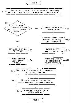
FIGURE 3 is a flow chart showing how equalization procedures are modified
21
CA 02267679 2003-12-22
.i
P54818PCT
in the FIGURE 1 DTV signal receiver depending on whether or not comb filtering
to
suppress co-channel NTSC interference is employed. The inventor points out
that the
presence of the artifacts of co-channel NTSC interference in the baseband
symbol
coding introduces errors into the calculation of equalization filter kernel
coefficients
unless special measures are taken in the calculations to negate these
artifacts.
In an initial step S1, a complex demodulation of digital television signals is
continuously performed by the complex demodulator 14 in the FIGURE 1 DTV
signal
receiver, to separate a received I-channel baseband signal and a received Q-
channel
baseband signal in an orthogonal relationship with the received I-channel
baseband
signal. In a decision step S2, which is also continuously performed by the
NTSC
co-channel interference detector 44 in the FIGURE 1 DTV signal receiver; it is
determined whether or not a significant amount of co-channel NTSC interference
accompanies-the received Q-channel baseband signal.
A significant amount of co-channel NTSC interference in a DTV signal
receiver is that level which causes the number of errors incurred during
trellis
decoding to significantly degrade the error correcting capabilities of the
two-dimensional Reed-Solomon decoding that follows trellis decoding, causing
substantial numbers of bit errors in the ultimately recovered data, under
conditions of
normally noisy reception. The significant amount of cb-channel NTSC
interference in
a DTV signal receiver .of particular design is readily determined by
experiments on a
prototype thereof.
If in the decision step S2 no significant amount of co-channel NTSC
interference is determined to accompany the received Q-channel baseband
signal, a
step S3 of adjusting the kernel weights of a digital equalization filter, in
order to
equalize its response to the I-channel baseband signal, and a subsequent step
S4 of
symbol decoding the equalization filter response resulting from the step S3
are
performed to generate symbol decoding result used in a step S5 of trellis
decoding the
symbol decoding result to correct errors therein. The step;S5 of trellis
decoding is
followed by a step S6 of Reed-Solomon decoding to coixect errors in the result
of
CA 02267679 2003-12-22
P54818PCT
trellis decoding and a step S7 of defonnatting the result of Reed-Solomon
decoding.
If in the decision step S2 a significant amount of co-channel NTSC
interference is determined to accompany the received Q-channel baseband
signal, a
step S8 of comb filtering the received I-channel baseband signal to generate
comb-filtered I-channel baseband signal is performed using a suitable comb
filter. In
a step S9 the kernel weights of the digital equalization filter are adjusted
to conform
the response of the cascaded digital equalization filter and comb filter to an
ideal
response for such filter cascade. A step SlO of symbol decoding the response
of such
filter cascade is performed and thereafter a step I1 of postcoding the symbol
decoding
I O response is performed to obtain corrected symbol decoding result to be
used in the
step SS of trellis decoding. The step SS of trellis decoding is still followed
by the step
'S6 of Reed-Solomon decoding to correct errors in the result of trellis
decoding and the
step S7 of deformatting the result of Reed-Solomon decoding.
The submethod used for adjusting the kernel weights of the digital
equalization filter in step S3 of equalizing digital equalization filter
response is
similar to the adjustment of the kernel weights of the digital equalization
filter used
in the prior art. Adjustment can be made by calculating the discrete Fourier
transform (DFT) of the received data field synchronization code or a
prescribed
portion thereof and dividing it by the DFT of tie ideal data freld
synchronization
code or prescribed portion thereof to determine the DFT of the DTV
transmission
channel. The DFT of the DTV transmission channel is normalized with respect to
the largest terms) to characterize the channel, and the kernel weights of the
digital
equalization filter are selected to complement the normalized DFT
characterizing
the channel. This method of adjustment is described in greater detail by C. B.
Patel
et alii in U. S. patent No: 5,331,416 issued 19 July 1994 and entitled
"METHODS
FOR OPERATING
GHOST-CANCELATION CIRCUITRY FOR TV RECEIVER OR VIDEO
RECORDER", for example. This method is preferable for initial adjustment of
the
kernel weights of the digital equalization filter because the'inifiial
adjustment is
more rapidly made than by using adaptive equalization. After initial
adjustment of
23
CA 02267679 2003-12-22
P54818PCT,
the kernel weights of the digital equalization filter, adaptive equalization
methods
are preferred. A block LMS method for carrying out adaptive equalization is
described by J. Yang et alii in U. S. patent No. 5,648,987 issued 15 July 1997
and
entitled "RAPID-UPDATE ADAPTIVE CHANNEL-EQUALIZATION
FILTERING FOR DIGITAL RADIO RECEIVERS, SUCH AS HDTV
RECEIVERS". A continuous LMS method for carrying out adaptive
equalization is described by A: L.R. Limberg in U.S. patent
No. 5,901,175 issued May 4, 1999 and entitled 'DYNAMICALLY
ADAPTIVE EQUALIZES SYSTEM ArrQ -METHOD' .
In the step S9 the submethod by which the kernel weights of the digital
equalization filter are adjusted to conform the response of the cascaded
digital.
equalization filter and comb filter to an ideal response for such filter
cascade can be
cazried out using DFT, especially when performing rapid initial equalization
prior to
switching to adaptive equalization. Adjustment is made by calculating the
discrete
Fourier transform (DFT) of the received data field synchronization code or a
prescribed portion thereof, as comb filtered by the comb filter 20 for
rejecting
NTSC artifacts and dividing it by the DFT of the ideal data field
synchronization
code or prescribed portion thereof, as so comb filtered, to determine the DFT
of the
DTV transmission channel. The DFT of the DTV transmission channel is then
normalized with respect to the largest terms) to characterize the channel, and
the
kernel weights of the digital equalization filter are adjusted to complement
the
normalized DFT characterizing the channel. After initial adjustment of the
kernel
weights of the digital equalization filter, adaptive equalization methods are
preferably employed. These adaptive equalization methods differ from those
used
when artifacts of NTSC co-channel interference are insignificant in that the
number
of possible valid signal states is doubled, less one, by using the comb filter
20 for
rejecting NTSC artifacts.
FIGURE 4 is a block schematic diagram showing details of a portion of the
FIGURE I DTV signal receiver using a species 120 of the NTSC-rejection comb
filter
20 and a species 126 of the postcoding comb filter 26. A subtractor 1202
serves as
24
~ 02267679 2003-12-22
P54818PCT
the first linear combiner in the NTSC-rejection comb filter 120, and a modulo-
8 adder
1262 serves as the second linear combiner in the postcoding comb filter x26.
The
NTSC-rejection comb filter 120 uses a first-delay device 1201 exhibiting a
delay of
twelve symbol epochs, and the postcoding comb filter 126 uses a second delay
device .
1263 also exhibiting a delay of twelve symbol epochs. The 12-symbol delay
exhibited by each of the delay devices 1201 and 1263 is close to one cycle
delay of
the artifact of the analog TV video earner at 59.75 times the analog TV
horizontal
scan frequency fH. The 12-symbol delay is close to five cycles of the artifact
of the ;
analog TV chrominance subcarrier at 287.25 times fH. The 12-symbol delay is
close
to six cycles of the artifact of the analog TV sound carrier at 345.75 times
fH. This is
the reason that the differentially combined response of the subtractor 1202 to
the
audio carrier, to the video carrier and to frequencies close to chrominance
subcarrier ,
differentially delayed by the first delay device I20I tends to have reduced co-
channel
interference. However, in portions of a video signal in which edges cross a
horizontal
scan line, the amount of correlation in the analog TV video signal at such
distances in
the horizontal spatial direction is quite low.
A species I26I of the multiplexer 26I is controlled by a multiplexer control
signal that is in its second state most of the time when it is determined
there is
insufficient NTSC co-channel interference to cause uncorrectable error in the
output
signal from the data-slicer 22 and that is in its third state most of the time
when it is
determined there is sufficient NTSC co-channel interference to cause
uncorrectable
error in the output signal from the data-slicer 22. The multiplexer I26I is
conditioned
by its control signal being in its third state to feed back the modulo-8 sum
results of
the adder 1262, as delayed twelve symbol epochs by the delay device I263, to
the
adder 1262 as a summand. This is a modular accumulation procedure in which a
single error propagates as a running error, with error recurring every twelve
symbol
epochs: Running errors in the postcoded symbol decoding results from the
postcoding comb filter 126 are curtailed by the multiplexer 1261 being placed
into its
first state for four symbol epochs at the beginning of each data segment, as
well as
during the entirety of each data segment containing field=aync. When this
control
~CA 02267679 2003-12-22
w~ r
P54818PCT
signal is in its first state, the multiplexes 1261 reproduces as its output
signal ideal
symbol decoding results supplied from memory in the controller 28. The
introduction
of ideal symbol decoding results into the multiplexes 1261 output signal halts
a
running error. Since there are 4 + 69(12} symbols per data segment; the ideal
symbol
decoding results slip back four symbol epochs in phase each data segment, so
no
running error can persist for longer than thxee data segments.
FIGURE S is a block schematic diagram showing details of a species 144 of
the FIGURE 2 NTSC co-channel interference detector 44 with a third delay
element
1442 therewithin providing a 12-symbol delay of Q-channel signal from the
symbol
synchronization and equalization circuitry I6 applied directly to the node
440. The
third linear combines is a digital subtractor 1443 differentially combining
differentially-delayed Q-channel signal from the symbol synchronization and
equalization circuitry 16 to generate the comb filter response supplied to the
amplitude detector 445 in which response artifacts of NTSC co-channel
interference
are rejected. The fourth linear combines is a digital adder 14.44.additively
combining
the differentially-delayed Q-channel signal to generate the comb filter
response
supplied to the amplitude detector 445 in which response artifacts of NTSC
co-channel interference are selected. This NTSC co-channel interference
detector 144
is especially well suited for use in the FIGURE.1 DTV signal receiver when it
uses
the species 120 of the NTSC-rejection comb filter 20 and the species ~I26 of
the
postcoding comb filter 26. Since the comb filtering employing the subtractor
1443
rejects artifacts arising from NTSC audio carrier, from NTSC video carrier and
from
NTSC color subcarrier the bandwidth selection filter 441 is unnecessary before
the
node 440.
FIGURE 6 is a block schematic diagram showing details of a portion of the
FIGURE 1 DTV signal receiver using a species 220 of the NTSC-rejection comb
filter
20 and a species 226 of the postcoding comb filter 26. The NTSC-rejection comb
f lter 220 uses a first delay device 2201 exhibiting a delay of six symbol
epochs, and
the postcoding comb filter 226 uses a second delay device~2263 also exhibiting
a
delay of six symbol epochs. The 6-symbol delay exhibited by each of the delay
26
CA 02267679 2003-12-22
P54818PCT
devices 2201 and 2263 is close to 0.5 cycle delay of the artifact of the
analog TV
video carrier at 59.75 times the analog TV horizontal scan frequency fH, close
to 2.5
cycles of the artifact of the analog~TV chrominance subcarrier at 287.25 times
fH, and
close to 3 cycles of any artifact of the analog TV audio carrier at 345.75
times fH. An
adder 2202 serves as the first linear combines in the NTSC-rejection comb
filter 220,
and.a modulo-8 subtractor 2262 serves as the second linear combines in the
postcoding comb filter 226. Since the delay exhibited by the delay devices
2201 and
2263 is shorter than the, delay exhibited by the delay devices 1201 and 1263,
although
nulls near frequencies converted from analog TV carrier frequencies are
narrower
band, there is more likely to be good anti-correlation in the signals
additively
combined by the adder 2202 than there is likely to be good correlation in the
signals
differentially combined by the subtractor 1202. The suppression of the sound
carrier
is poorer in the NTSC-rejection comb filter 220 response than in the NTSC-
rejection '
comb filter 120 response. However, if the sound carrier of a co-channel
interfering
analog TV signal has been suppressed by SAW filtering or a sound trap in the
IF
amplifier chain 12, the poor sound rejection of the comb filter 220 is not a
problem.
The responses to sync tips is reduced in duration using the NTSC-rejection
comb filter
220 of FIGURE 6 rather than the NTSC-rejection comb filter 120 of FIGURE 4, so
there is substantially reduced tendency to overwhelm error-correction in the
trellis
decoding and Reed-Solomon coding.
A species 2261 of the multiplexes 261 is controlled by a multiplexes control
signal that is in its second state most of the time when it is determined
there is
insufficient NTSC co-channel interference to cause uncorrectable error in the
output
signal from the data-slices 22 and that is in its third state most of the time
when it is
determined there is sufficient NTSC co-channel interference to cause
uncorrecfable
error in the output signal from the data-slices 22. The multiplexes 2261 is
conditioned
by its control signal being in its third state to feed back the modulo-8 sum
results of
the adder 2262, as delayed six symbol epochs by the delay device 2263, to the
adder
2262 as a summand. This is a modular accumulation procedure in which a single
~ error propagates as a running error, with error recurrin~'every six symbol.
epochs.
27
CA 02267679 2003-12-22
P5481BPCT
Running errors in the postcoded symbol decoding results from the postcoding
comb
filter 226 are curtailed by the multiplexer 2261 being placed into its first
state for four
symbol epochs at the beginning of each data segment, as well as during the
entirety of
each data segment containing field sync. When this control signal is in its
first state,
the multiplexer 2261 reproduces as its output signal ideal symbol decoding
results
supplied from memory in the controller 28. The introduction of ideal symbol
decoding results into the multiplexer 2261 output signal halts a running
error. Since
there are 4 + 138(6) symbols per data segment, the ideal symbol decoding
results slip
back four symbol epochs in phase each data segment, so no running error can
persist
for longer than two data segments. The likelihood of a protracted period of
running
error in the postcoding comb filter 226 is substantially less than in the
postcoding
comb filter 126, although the running error recurs more frequently and affects
twice as
many of the twelve interleaved trellis codes.
FIGURE 7 is a block~schematic diagram showing details of a species 244 of
the FIGURE 2 NTSC co-channel interference detector 44 with a third delay
element
2442 therewithin providing a 6-symbol delay to Q-channel signal applied to the
node
440. The third linear combiner is a digital adder 2443 additively combining
the
differentially-delayed Q-channel signal to generate the comb filter response
supplied
to the amplitude detector 445 in which response artifacts of NTS C co-channel
interference axe rejected. The fourth linear combiner is a digital subtractor
2444
differentially combining differentially-delayed Q-channel signal from the
symbol
synchronization and equalization circuitry 7.6 to generate the comb filter
response
supplied to the amplitude detector 446 in which response artifacts of NTSC co-
channel interference are selected. This NTSC co-channel interference detector
244 is
especially well suited for use in the FIGURE 1 DTV signal receiver when it
uses the
species 220 of the NTSC-rejection comb filter 20 and the species 226 of the
postcoding comb filter 26.
FIGURE 8 is a block schematic diagram showing details of a portion of the
FIGURE I DTV signal receiver using a species 320 of the NTSC-rejection comb
filter
' 20 and a species 326 of the postcoding comb filter 26. The NTSC-rejection
comb
2.8
CA 02267679 2003-12-22
P54818PCT
filter 320 uses a first delay device 3201 exhibiting a delay of 13b8 symbol
epochs,
which delay is substantially equal to the epoch of. two horizontal scan lines
of an
analog TV signal, and the postcoding comb filter326 uses a second delay device
3263
also exhibiting such delay. The first linear combines in the NTSC-rejection
comb
filter 320 is an adder 3202, and the second linear combines in the postcoding
comb
filter 326 is a modulo-8 subtractor 3262.
A species 3261 of the multiplexes 261 is controlled by a multiplexes control
signal that is in its second state most of the time when it is determined
there is
insufficient NTSC co-channel interference to cause uncorrectable error in the
output
signal from the data-slices 22 and that is in its third state most of the time
when it is
determined there is sufficient NTSC co-channel interference to cause
uncorrectable
error in the output signal from the data-slices 22. The DTV signal receiver
preferably
contains circuitry for detecting change between alternate scan lines in the
NTSC
co-channel interference, so that the controller 28 can withhold supplying the
third
state of the multiplexes 3261 control signal under such conditions.
The multiplexes 3261 is conditioned by its control signal being in its third
state to feed back the modulo-8 sum results of the adder 3262, as delayed 1368
symbol epochs by the delay device 3263, to the adder 3262 as a summand. This
is a
modular accumulation procedure in which a single ez-ror propagates as a
running error,
with error recurring every 1368 symbol epochs. This symbol code span is longer
than
the span for a single block of the Reed-Solomon code, so a single running
error is
readily corrected during Reed-Solomon decoding. Running errors in the
postcoded
symbol decoding~results from the postcoding comb filter 326 are curtailed by
the
multiplexes 3261 being placed into its first state during the entirety of each
data
segment containing freld sync, as well as for four symbol epochs at the
beginning of
each data segment. When this control signal is in its first state, the
multiplexes 3261
reproduces as its output signal ideal symbol decoding results supplied from
memory
~in the controller 28. The introduction of ideal symbol decoding results into
the
multiplexes 3261 output signal halts a rum-~ing error. T~,e~16.67 millisecond
duration
of an NTSC video field exhibits phase slippage against the 24. l9 millisecond
duration
29
CA 02267679 2003-12-22
P54818PCT
of a DTV data field, so the DTV data segments' containing field sync
eventually scan
the entire NTSC frame raster. The 525 lines in the NTSC frame raster each
contain
684 symbol epochs, for a total of 359,100 symbol epochs. Since this is
somewhat less
than 432 times the 832. symbol epochs in a DTV data segment containing field
sync,
one can guess with reasonable confidence that running errors of duration
longer than
' 432 data fields will be expunged by the multiplexer 3261 reproducing ideal
symbol
decoding results during DTV data segments containing field sync. There is also
phase
slippage between data segments, for the.start code groups of which ideal
symbol
decoding results are available, and NTSC video scan lines. One can estimate
359,100
symbol epochs, which is 89,775 times the four symbol epochs iri a code start
group,
are scanned during 89,775 consecutive data segments. Since there are 3I3 data
segments per DTV data field, one can guess with reasonable confidence that
running
errors of duration longer than 287 data fields will -be expunged by the
multiplexer
3261 reproducing ideal symbol decoding results during the code start groups.
The
two sources of suppression of running errors are reasonably independent of
each
other, so running errors of duration longer than two hundred or so data fields
are quite
unlikely.. Furthermore; if NTSC co-channel interference dips low at a time
when the
running error recurs, to condition the multiplexer 3261 for reproducing the
response
of the data-slicer 22 as its output signal, the error may be corrected earlier
than would
otherwise be the case. . w
The FIGURE 8 NTSC-rejection comb filter 320 is quite good in suppressing
demodulation artifacts generated in response to analog TV horizontal
synchronizing
pulses, as well as suppressing many of the demodulation artifacts generated in
response to analog TV vertical synchronizing pulses and equalizing pulses.
These
artifacts are the co-channel interference with highest energy. Except where
there is
scan-line-to-scan-Line change in the video content of the analog TV signal
over the
period of two scan lines, the NTSC-rejection comb filter 320 provides
reasonably
good suppression of that video content regardless of its color. The
suppression of the
FM audio carrier of the analog TV signal is reasonably good, in case it has
not been
suppressed by a tracking rejection filter in the symbol synchronization and
CA 02267679 2003-12-22
P54818PCT
equalization circuitry 16. Artifacts of most analog TV color bursts are
suppressed in
the NTSC-rejection comb filter 320 response, too.. Furthermore, the filtering
provided
by the NTSC-rejection comb filter 320 is "orthogonal" to the NTSC-interference
rejection built into the trellis decoding procedures.
FIGURE 9 is a block schematic diagram showing details of a species 344 of
the FIGURE 2 NTSC co-channel interference detector 44 with a third delay
element
3442 there~;vithin providing a 2-video-Iine delay of 1368 symbol epochs to Q-
channel
signal applied to the node 440. The third linear combiner is a digital adder
3443
additively combining the differentially-delayed Q-channel signal to generate
the comb
filter response supplied to the amplitude detector 445 in which response
artifacts of
NTSC co-channel interference are rejected. The fourth linear combiner is a
digital
subtractor 3444 differentially combining differentially-delayed Q-channel
signal from
the symbol synchronization and equalization circuitry 16 to generate the comb
filter
response supplied to the amplitude detector 446 in which response artifacts of
NTSC
I S co-channel interference are selected. This NTSC co-channel interference
detector 344
is especially well suited for use in the FIGURE 1 DTV signal receiver when it
uses
the species 320 of the NTSC-rejection comb filter 20 and the species 326 of
the
postcoding comb filter 26.
FIGURE 10 is a block schematic diagram showing details of a'portion of the
FIGURE 1 DTV signal receiver using a species 420 of the NTSC-rejection comb
filter
20 and a species 426 of the postcoding comb filter 26. The NTSC-rejection comb
filter 420 uses a first delay device 4201 exhibiting a delay of 179,208 symbol
epochs,
which delay is substantially equal to the period of 262 horizontal scanning
lines of an
analog TV signal, and the postcoding comb filter 426 uses a second delay
device 4261
also exhibiting such delay. An adder 4202 serves as the first linear combiner
in the
NTSC-rejection comb filter 420, and a modulo-8 subtractor 4262 serves as the
second
linear combiner in the postcoding comb filter 426.
A species 4261 of the multiplexer 261 is controlled by ~ multiplexer control
signal that is in its second state most of the time when it'is determined
there is
31
CA 02267679 2003-12-22
a ..
,,
P54818PCT
insufficient NTSC co-channel interference to cause uncorrectable error in the
output
signal from the data-slices 22 and that is in its third state most of the time
when it is
determined there is sufficient NTSC co-channel interference to cause
uncorrectable
error in the output signal from the data-slices 22.. The DTV signal receiver
preferably
contains circuitry for detecting field-to-field change in the NTSC co-channel
' interference, so that the controller 28 can withhold supplying the third
state of the
multiplexes 4261 control signal under such conditions.
The multiplexes 4261 is conditioned by its control signal being in its third
state to feed back the modulo-8 sum results of the adder 4262, as delayed
179,208
symbol epochs by the delay device 4263, to the adder 4262 as a summand. This
is a
modular accumulation procedure in which a single error propagates as a running
error,
with error recurring every 179,208 symbol epochs. This symbol code span is
longer
than the span for a single block of the Reed-Solomon code, so a single running
error is
readily corrected during Reed-Solomon decoding. Running errors in the
postcoded
symbol decoding results from the postcoding comb filter 426 are curtailed by
the
multiplexes 4261 being placed into its first state during the entirety of each
data
segment containing field sync, as well as for four symbol epochs at the
beginning of
each data segment. When this control signal is in its first state, the
multiplexes 4261
reproduces as its output signal ideal symbol decoding results supplied from
memory
in the controller 28. The introduction of ideal symbol decoding results into
the
multiplexes 4261 output signal halts a running error. The maximum number of
data
fields required to expunge running error in the multiplexes 4261 output signal
is
presumably substantially the same as required to expunge running error in the
multiplexes 3261 output signal. .However, the number of times the error recurs
in that
period is lower by a factor of 131.
The FIGURE 10 NTSC-rejection comb filter 420 suppresses most
demodulation artifacts generated in response to analog TV vertical
synchronizing
pulses and equalizing pulses, as well as suppressing alI the demodulation
artifacts
generated in response to analog TV horizontal synchron.lzing pulses. These
artifacts
are the co-channel interference with highest energy. Also, the NTSC-rejection
comb
32
CA 02267679 2003-12-22
a
r
P54818PCT
filter 420 suppresses artifacts arising from the video content of the analog
TV signal
that does not change from field to field or line-to-line, getting rid of
stationary
pattern's irrespective of their horizontal spatial frequency or color.
Artifacts of most
analog TV color bursts are suppressed in the NT$C-rejection comb flter 420
response, too.
FIGURE 11 is a block schematic diagram showing details of a species 444 of
the FIGURE 2~NTSC co-channel interference detector 44 with a third delay
element
4442 therewithin providing a 262-video-line delay of 179,208 symbol epochs to
Q-channel signal applied to the node 440. The third linear combiner is a
digital adder
4443 additively combining the differentially-delayed Q-channel signal to
generate the
comb filter response supplied to the amplitude detector 445 in which response
artifacts of NTSC co-channel interference are rejected. The fourth linear
combiner is
a digital subtractor 4444 differentially combining differentially-delayed Q-
channel
signal from the symbol synchronization and equalization circuitry 16 to
generate the
comb filter response supplied to the amplitude detector 446 in which response -
~.
artifacts ofNTSC co-channel interference are selected. This NTSC co--channel
interference detector 444 is especially well suited for use in the FIGURE 1
DTV
signal receiver when it uses the species 420 of the NTSC-rejection comb filter
20 and
the species 426 of the postcoding comb filter 26.
FIGURE 12 is a block schematic diagram showing details of a portion of the
FIGURE 1 DTV signal receiver using a species 520 of the NTSC-rejection comb
filter
20 and a species 526 of the postcoding comb filter 26. The NTSG-rejection comb
filter 520 uses a first delay device 5201 exhibiting a delay of 718,200 symbol
epochs,
which delay is substantially equal to the period of two frames of an analog TV
signal,
and the postcoding comb filter 526 uses a second delay device 5261 also
exhibiting
such delay. A subtractor 5202 serves as the first linear combiner in the
NTSC-rejection comb filter 520, and a modulo-8 adder 5262 serves as the second
linear combiner in the postcoding comb filter 526.
., y
A species 5261 of the multiplexer 261 is controlled by a multiplexer control
., .,
CA 02267679 2003-12-22
P
P t
P54818PCT
signal that is in its second state most of the time when it is determined
there is
insufficient NTSC co-channel interference to cause uncorrectable error in the
output
signal from the data-slices 22 and that is irl its third state most of the
time when it is
determined there is sufficient NTSC co-channel interference to cause
uncorrectable
error in the output signal from the data-slices 22. The DTV signal receiver
preferably
' contains circuitry for detecting change between alternate frames in the NTSC
co-channel interference; so that the controller 28 can withhold supplying the
third
state of the multiplexes 5261 control signal under such conditions.
The multiplexes 5261 is. conditioned by its control signal. being in its third
state to feed back the modulo-8 sum results of the adder 5262, as delayed
718,200
symbol epochs by the delay device 5263, to the adder 5262 as a summand. This
is a
modular accumulation procedure in which a single error propagates as a running
error,
with error recurring every 718,200 symbol epochs. This symbol code span is
longer
than the span for a single block of the Reed-Solomon code, so a single running
error is
readily corrected during Reed-Solomon decoding. Running errors in the
postcoded
symbol decoding results from the postcoding comb filter 526 are curtailed by
the
multiplexes 5261 being placed into its first state during the entirety of each
data
segment containing field sync, as well as for four symbol epochs at the
beginning of
each data segment. When this control signal zs in its first state, the
multiplexes 5261
reproduces as its output signal ideal symbol decoding results supplied from
memory
in the controller 28. The introduction of ideal symbol decoding results into
the
multiplexes 5261 output signal halts a running error. The maximum number of
data
fields required to expunge running ezror in the multiplexes 5261 output signal
is
presumably substantially the same as required to expunge running error in the
multiplexes 3261 output signal. However, the number of times the error recurs
in that
period is lower by a factor of 525.
The FIGURE 12 NTSC-rejection comb filter 520 suppresses all demodulation
artifacts generated in response to analog TV vertical synchronizing pulses and
equalizing pulses, as well as suppressing all the demodulation artifacts
generated in
response to analog TV horizontal synchronizing pulses. These artifacts are the
34
CA 02267679 2003-12-22
a
h
P54818PCT
co-channel interference with highest energy. AIso, the NTSC-rejection comb
filter
520 suppresses artifacts arising from the video content of the analog TV
signal that
does not change over two frames, getting rid of such very stationary patterns
irrespective of their spatial frequency or color. Artifacts of alI analog TV
color bursts
are suppressed in the NTSC-rejection comb filter 520 response, too.
FIGURE 13 is a block schematic diagram showing details of a species 544 of.
the FIGURE 2 NTSC co-channel interference detector 44 with a third delay
element ,
5442 therewithin providing a 2-video-frame delay of 718,200 symbol epochs to Q-
channel signal applied to the node 440. The third linear combiner is a digital
adder
5443 additively combining the differentially-delayed Q-channel signal to
generate the
comb filter response supplied to the amplitude detector 445 in which response
artifacts of NTSC co-channel interference are rejected. The fourth linear
combiner is
a digital subtractor 5444 differentially combining differentially-delayed Q-
channel
signal-from the symbol synchronization and equalization circuitry 16 to
generate the
comb filter response supplied to the amplitude detector 446 in which response
artifacts of NTSC co-channel interference are selected. This NTSC co-channel
interference detector 544 is especially well suited for use in the FIGURE 1
DTV
signal receiver when it uses the species 520 of the NTSC-rejection comb filter
20 and
the species 526 of the postcoding comb filter 26: ,
One skilled in the art of television system design will discern other
properties
of correlation and anti-correlation in analog TV signals that can be exploited
in the
design of NTSC-rejection filters of still other types than those shown in
FIGURES
4, 6, 8, 10 and 12. The use of NTSC-rejection filters that cascade two NTSC-
rejection
filters of the types already disclosed increases the 2N levels of the baseband
signals to
(8N-1) data Levels, which increases the difficulty of data slicing during
symbol
decoding. Such filters may be required to overcome.particularly bad co-channel
interference problems despite their shortcoming of reducing signal-to-noise
for
random noise interference ~,vith symbol decoding. Cascading,filters to improve
NTSC
rejection and selection in the co-channel interference detector has less
drawback
associated with it.
3~
CA 02267679 2003-12-22
..
P54818FCT
FIGURE 14 illustrates cascading of filters to improve NTSC rejection and
selection in a species 644 of the co-channel interference detector 44 that can
be
considered to be a modification of the FIGURE 13 co-channel interference
detector
544. The response of the FIR digital lowpass filter 44x0 to equalized Q-
channel
S signal from the symbol synchronization and equalization circuitry 16 is
applied to the
node 440. There is a saving in hardware if the comb filter section requiring
the
longest delay is earliest in the cascade, since the same longest delay element
can be
used both by the NTSC-reject comb filter and by the NTSC-select comb filter.
As in '
the FIGURE 13 co-channel interference detector 544, the signal at the node 440
is
supplied to the 2-video-frame delay element 5442 in the FIGURE 14 co-channel
interference detector 644; and the resulting differentially delayed signals
are
additively combined by the adder 5443 and differentially combined by the
subtractor
5444.
The sum response from the adder 5443 is subjected to further NTSC-rejection
1 S filtering to generate the NTSC-rejection comb filter response supplied to
the
amplitude detector 445. More particularly, a delay device 6441 provides 6-
symbol
differential delay to the sum response from the adder 5443, and the
differentially
delayed sum responses from the adder 5443 are additively combined by a digital
adder 6442 to generate the NTSC-rejection cbmb filter response supplied to the
amplitude detector 445.
The difference response from the subtractor 5444 is subjected to further
NTSC-rejection filtering to generate the NTSC-selection comb filter response
supplied to the amplitude detector 446. More particularly, a delay device 6443
provides 6-symbol differential delay to the difference response from the
subtractor
5444, and the differentially delayed difference responses from the subtractor
5444 are
differentially combined by a digital subtractor 6444 to generate the NTSC-
selection
comb filter response supplied to the amplitude detector 446. The results of
amplitude
detection by the amplitude detectors 445 and 446 are compared by an amplitude
comparator 447. The amplitude comparator 447 supplies an output bit indicative
of
whether or not the response of the amplitude detector 446 substantially
exceeds the
3G
CA 02267679 2003-12-22
,. r r
P54.818PCT
response of the amplitude detector 445. This output bit is used for selecting
between
the second and third states of multiplexer 261 operation in the FIGURE 1 DTV
signal
receiver which uses the co-channel interference detector 644 as its co-channel
interference detector 44. The cascade filtering in, the co-channel
interference detector
644 utilizes the temporal comb filtering between alternative NTSC video frames
to
' suppress NTSC artifacts arising from synchronizing information and static
video
components. The cascade filtering in the co-channel interference detector 644
utilizes
intraframe spatial comb.filtering to suppress NTSC artifacts arising from
dynamic
video components.
FIGURE 15 further illustrates cascading of filters to improve NTSC rejection
and selection in another species 744 of the co-channel interference detector
44 that
can be considered to be a modification of the FIGURE 13 co-channel
interference
detector 544. The equalized Q-channel signal from the symbol synchronization
and
equalization circuitry 16 is applied directly to the node 440, the FIR digital
lowpass
filter 4410 being unnecessary since the second stage of comb f ltering
suppresses
artifacts of the audio carrier of any co-channel interfering NTSC analog TV
signal. A
s in the FIGURE 13 co-channel interference detector 544, the signal at the
node 440 is
supplied to the 2-video-frame delay element 5442 in the FIGURE 1 S co-channel
interference detector 644; and the resulting differentially delayed signals
are
additively combined by the adder 5443 and differentially combined by the
subtractor
5444.
The sum response from the adder 5443 is subjected to further NTSC-rejection
filtering to generate the NTSC-rejection comb filter response supplied to the
amplitude detector 445. More particularly, a delay device 7441 pzovides 12-
symbol
differential delay to the sum response from the adder 5443, and the
differentially
delayed sum responses from the adder 5443 are differentially combined by a
digital
subtractor 7442 to generate the NTSC-rejection comb filter response supplied
to the
amplitude detector 445.
The difference response from the subtractor 544. is subjected to further
37
CA 02267679 2003-12-22
r. s
P548i8PCT
NTSC-rejection filtering to generate the NTSC-selection comb filter response
supplied to the amplitude detector 446: More particularly, a delay device 7443
provides 12-symbol differential delay to the difference response from the
subtractor
5444, and the differentially delayed difference responses from the subtractor
5444 are
additively combined by a digital adder 7444 to generate the NTSC-selection
comb
' filter response supplied to the amplitude detector 446. The results of
amplitude
detection by the amplitude detectors 445 and 446 are compared by an amplitude
comparator 447. The amplitude comparator 447 supplies an output bit indicative
of
whether or not the response of the amplitude detector 446 substantially
exceeds the
response of the amplitude detector 445. This output bit is used for selecting
between
the second and third states of multiplexes 261 operation in the FIGURE 1 DTV
signal
receiver which uses the co-channel interference detector 744 as its co-channel
interference detector 44. The cascade filtering in the co-channel interference
detector
744 utilizes the temporal comb filtering between alternative NTSC video frames
to
suppress NTSC artifacts arising from synchronizing information and static
video
components. The cascade filtering in the co-channel interference detector 744
utilizes
intraframe spatial comb filtering to suppress NTSC artifacts arising from
audio
components and dynamic video components,
FIGURE 16 shows modification of the FIGURE 1 DTV signal receiver as
thusfar described, constructed in accordance with a further aspect of the
invention so
as to utilize a plurality of parallelly operated even-level data slicers A24,
B24 and
C24, each preceded by a respective NTSC-rejection comb filter and succeeded by
a
respective postcoding comb filter. The even-level data-slices A24 converts the
response of an NTSC-rejection filter A20 of a first type to first precoded
symbol
decoding results for application to a postcoding comb filter A26 of a first
type. The
even-level data-slices B24 converts the response of an NTSC-rejection filter
B20 of a
second type to second precoded symbol decoding results for application to a
postcoding comb filter B26 of a second type. The even-level data-slices C24
converts
the response of an NTSC-rejection filter C20 of a third type tb third precoded
symbol
decoding results for application to a postcodin~ comb filter C26 of a third
type: The
Jc
CA 02267679 2003-12-22
e~
r " .
P54818PCT
f
odd-level data-slicer Z2 supplies interim symbol decoding results to the
postcoding
comb filters A26, B26 and C26. The prefixes A, B and C in the identification
numbers for the elements of FIGURE 15 are different integers which will
correspond
to respective ones of the integers 1, 2, 3, 4 and S when receiver portions as
shown in
ones of FIGURES 4, 6, 8, 10 and 12 are employed.
A co-channel interference detector A44 of a first type determines from the
Q-channel signal how effective the NTSC-rejection filter A20 of first type
will be in
reducing co-channel interference from an analog TV signal in the current.
equalized
I-channel signal. A co-channel interference detector B44 of a second type
determines
from the Q-channel signal how effective the NTSC-rejection filter B20 of
second type
will be in reducing co-channel interference from an analog TV signal in the
current
equalized I-channel signal. A co-channel interference detector C44 of a third
type
determines from the Q-channel signal how effective the NTSC-rejection filter
C20 of
third type will be in reducing co-channel interference from an analog TV
signal in the
current equalized I-channel signal. The suppression of the pilot'carrier in
the
Q-channel signal facilitates the co-channel interference detectors A44, B44
and C44
providing indications of the relative effectiveness of the NTSC-rejection comb
filters
A20, B20 and C20.
Syrribol decoding selection circuitry 90 generates a best estimate of correct
symbol decoding for application to the data assembler 30. This best estimate
is
generated by selecting among ideal symbol decoding results from the controller
28,
interim symbol decoding results from the odd-level data slicer 22, and
postcoded
symbol decoding results from the postcoding comb filters A26, 826 and C26. The
symbol decoding selection circuitry 90 responds to indications of
effectiveness from
the co-channel interference detectors A44, B44 and C44 to formulate this best
estimate unless the controller 28 supplies further symbol selection
information to the
symbol decoding selection circuitry 90. The further symbol selection
information -
supplied from the controller 28 includes indications of when synchronizing
codes
occur, which indications condition the best estimate to tie made based on
ideal symbol
decoding results from the controller 28. The best estimate of symbol decoding
results
39
CA 02267679 2003-12-22
,. , a
P54818PCT
is used to correct the summation procedures in the matching comb filters A26,
B26
and C26 in preferred embodiments of the FIGURE 16 DTV signal receiver .
If the co-channel interference detectors A44, B44 and C44 all indicate lack of
substantial artifacts from NTSC co-channel interference at times other than
when
f5 synchronizing codes occur, the symbol decoding selection circuitry 90
responds to
select the interim symbol decoding results from the odd-level data slicer 22
as the best
estimate of correct symbol decoding results. This minimizes the effect of
Johnson
noise on symbol decoding.
If at least one of the co-channel interference detectors A44, B44 and C44
indicates substantial artifacts from NTSC co-channel interference at times
other than
when synchronizing codes occur, the symbol decoding selection circuitry 90
responds to select the postcoded symbol decoding results from the postcoding
comb
filter A26, B26 or C26 following the one of the NTSC-rejection corizb filters
A20,
B20 and C20 that best suppresses artifacts from NTSC co-channel interference
as
determined by the co-channel interference detectors A44, B44 and C44.
The high-energy demodulation artifacts generated in response to analog TV
synchronizing pulses, equalizing pulses, and color bursts are all suppressed
when the
NTSC-rejection comb filter A20 additively combines alternate video frames.
Also,
artifacts arising from the video content of the analog TV signal that does not
change
over two frames, are suppressed, getting rid of stationary patterns
irrespective of their
spatial frequency or color. The co-channel interference detector A44 of FIGURE
13
is used together with the FIGURE 12 symbol decoding circuitry.
The remaining problem of suppressing demodulation artifacts primarily
concerns suppressing those demodulation artifacts arising from frame-to-frame
difference at certain pixel locations within the analog TV signal raster.
These
demodulation artifacts can be suppressed by intra-frame filtering techniques.
The
NTSC-rejection comb filter B20 and the postcoding comb filter B26 circuitry
can be
chosen to suppress remnant demodulation artifacts by belying on correlation in
the
horizontal direction, and the NTSC-rejection comb filter C20 and the
postcoding
CA 02267679 2003-12-22
r~. t
P54818PCT
comb filter C26 circuitry can be chosen to suppress remnant demodulation
artifacts by
relying on correlation in the vertical direction. Consider how such a design
decision
can be further implemented.
If the sound carrier of a co-channel interfering analog TV signal is not
S suppressed by SAW filtering or a sound trap in the IF amplifier chain 12,
the
NTSC-rejection comb filter B20 and the postcoding comb filter B26 circuitry
are
advantageously chosen to be of types like the NTSC-rejection comb filter x20
and the
postcoding comb filter 126 circuitry'of FIGURE 4. The co-channel interference
detector B44 of FIGURE 5 is used together ~,vith the FIGURE 4 symbol decoding
circuitry.
If the sound carrier of a co-channel interfering analog TV signal is
suppressed
by SAW filtering or a sound trap in the IF amplifier chain 12, the NTSC-
rejection
comb filter B20 and the postcoding comb filter B26 circuitry are
advantageously
chosen to be of types like the NTSC-rejection comb filter 220 and the
postcoding
comb filter 226 circuitry of FIGURE 6. This is because the anti-correlation
between
video components only six symbol epochs away from each other is usually better
than
the correlation between video components twelve symbol epochs away from each
other. The co-channel interference detector B44 of FIGURE 7 is used together
with
the FIGURE 6 symbol decoding circuitry.
The optimal choice of the NTSC-rejection comb filter C20 and the postcoding
comb filter C26 circuitry is less straightforward, because of the choice one
must make
(in consideration of field interlace in the interfering analog TV signal)
whether to
choose the temporally closer scan line in the same field or the spatially
closer line in
the preceding field to be combined with the current scan line in the NTSC-
rejection
comb filter C20. Choosing the temporally closer scan line in the same field is
generally the better choice, since jump cuts between fields are less likely to
ravage
NTSC rejection by the comb filter C20. With such choice, the NTSC-rejection
comb
filter C20 and the postcoding comb filter C26 circuitry are of types like the
NTSC-rejection comb filter 320 and the postcoding comb filter 326 circuitry of
41
CA 02267679 2003-12-22
:r
~,.
P54818PCT
FIGURE 8. The co-channel interference detector C44 of FIGURE 9 is used
together
with the FIGURE 8 symbol decoding circuitry.
With the other choice instead, the NTSC-rejection comb filter C20 and the
postcoding comb filter C26 circuitry are of types like the NTSC-rejection comb
filter
420 and the postcoding comb filter 426 circuitry of FIGURE I0. The ~co-channel
interference detector C44 of FIGURE I 1 is used together with the FIGURE 10
symbol decoding circuitry.
.. ::,
42