Note: Descriptions are shown in the official language in which they were submitted.
CA 02267723 1999-03-24
BOOST CONVERTER HAZTING REDUCED OUTPUT VOLTAGE AND
METHOD OF OPERATION THEREOF
TECHNICAL FIELD OF THE INVENTION
The present invention is directed, in general, to
power conversion and, more specifically, to a three-phase
boost converter having a reduced output voltage and a
method of operating the same.
BACKGROUND OF THE INVENTION
Regulated DC power supplies are typically needed for
most analog and digital electronic systems. Two major
categories of regulated DC power supplies are linear
power supplies and switching power supplies. Generally,
in linear power supplies, to provide electrical isolation
between an input and an output and to provide the output
in a desired voltage range, a transistor (operating in
its active region) is connected in series with a
transformer, e.g., a 60-Hz transformer.
In switching power supplies, transformation of DC
voltage from one level to another is accomplished
typically with DC/DC converter circuits, such as a step
down (buck) or step-up (boost) circuit. Solid-state
devices, such as transistors, are operated as switches
(either completely ON or completely OFF) within these
switching converters. Since the power devices are not
required to operate in their active region, this mode of
operation results in lower power dissipation.
Furthermore, increasing switching speeds, higher voltage
and current ratings of these power devices are some of
the factors that have increased the popularity of
switching power supplies.
For applications requiring three phase off-line
CA 02267723 1999-03-24
2
rectification with low input current total harmonic
distortions (THDs), the simplest switching power
converter topology is a single switch discontinuous
current mode (DCM) boost converter. By operating the
boost converter's three input inductors in DCM, at the
beginning of each switching cycle when the boost switch
is ON, currents through the input inductors begin to ramp
up from an initial value of zero at a rate that is
proportional to the input inductors corresponding phase
to neutral voltage. Consequently, the input inductor
currents, which are also the phase currents, are
naturally proportional to their corresponding phase
voltages during the period when the boost switch is ON.
When the boost switch is OFF, an output voltage that is
higher than the peak of the input phase-to-phase voltage
will drive the input inductors' currents to reduce back
to zero prior to the initiation of the next switching
cycle. The rate of decrease of each input inductor's
current, however, is not proportional to its
corresponding input phase-to-neutral voltage due to the
different amounts of energy that had been stored in each
input inductor. As a result, the input inductor currents
during the period when the boost switch is OFF are also
not proportional to the input inductors' corresponding
phase-to-neutral voltages resulting in distortions in the
input phase currents. It should be noted that the higher
the output voltage is, the faster are the individual
input inductor currents' rate of decrease. The faster
the input inductor currents are decreased to zero has the
corresponding benefit of reducing the distortions in the
input currents.
Studies have shown that to achieve a total harmonic
distortion (THD) of less than 10~, the output voltage is
CA 02267723 1999-03-24
3
required to be greater than 1.7 times the input phase-to-
phase peak voltage (M > 1.7; where M = Vout/Vin(rms)).
This high output voltage requirement for a low THD
normally results in an output voltage that is higher than
what is generally desired. For example, for an input
voltage 208 Vrms and taking into account the presence of
input voltage fluctuations, the output voltage would be
required to be about 650 V to realize THDs of less than
10%. This 650 V output voltage is much higher than a 440
V output that is normally desired. For an input voltage
of 440 Vrms, the required output voltage would then have
to be as high as 1300 V (far above a conventional 800 V
output) to achieve THDs of less than 10%.
Accordingly, what is needed in the art is an
improved power converter that overcomes the above
described limitations. More specifically, what is needed
in the art is a power converter with a low output to
input voltage ratio with the inherent low THD
characteristics of a power converter with a high output
to input voltage ratio (M > 1.7).
SUNJNiARY OF TI3E INVENTTON
To address the above-discussed deficiencies of the
prior art, the present invention provides, for use with
a boost converter having a three phase rectifier, a boost
switch coupled across the rectifier and a boost diode,
operable in discontinuous mode, coupled between the
rectifier and an output of the boost converter, a circuit
for, and method of, providing a reduced output voltage
from the boost converter. In one embodiment, the circuit
includes an autotransformer, coupled across the output,
that has an intermediate tap for providing the reduced
output voltage.
CA 02267723 1999-03-24
4
The present invention therefore introduces the broad
concept of employing an autotransformer to reduce a boost
converter's output voltage. The present invention
discloses a novel circuit that takes advantage of the low
THD inherent in a boost converter with high M, e.g., M >
1.7. The present invention introduces a circuit at the
output stage of the boost converter that provides an
output voltage that is at a desired lower value while
still enjoying the low THD provided by the boost
operation.
In one embodiment of the present invention, the
circuit further includes an output capacitor, coupled to
the intermediate tap, that attenuates a DC component in
the reduced output voltage. Those skilled in the art are
familiar with output capacitors and their function in
providing a DC output in boost converters.
In one embodiment of the present invention, the
intermediate tap is a center tap of the autotransformer.
Alternatively, the intermediate tap may not "bisect" the
windings of the autotransformer.
In one embodiment of the present invention, the
circuit further includes a snubber circuit, coupled to
the boost switch, that clamps a voltage overshoot
occurring therein. In a more specific embodiment, the
snubber circuit is a passive snubber circuit.
Alternatively, the snubber circuit may be an active
snubber circuit. The present invention does not,
however, require a snubber circuit.
In one embodiment of the present invention, the
autotransformer comprises windings having equal numbers
of turns. The windings may alternatively differ in
numbers of turns. The present invention is not limited
to a particular turns-ratio.
CA 02267723 1999-03-24
S
In one embodiment of the present invention, the
circuit further includes a diode series-coupled with the
autotransformer across the output. The diode rectifies
power through the autotransformer. Alternatively, an
active switch can perform the function if it is desired
in a particular application.
The foregoing has outlined, rather broadly,
preferred and alternative features of the present
invention so that those skilled in the art may better
understand the detailed description of the invention that
follows. Additional features of the invention will be
described hereinafter that form the subject of the claims
of the invention. Those skilled in the art should
appreciate that they can readily use the disclosed
conception and specific embodiment as a basis for
designing or modifying other structures for carrying out
the same purposes of the present invention. Those
skilled in the art should also realize that such
equivalent constructions do not depart from the spirit
and scope of the invention in its broadest form.
BRIEF DESCRIPTION OF THE DRAWINGS
For a more complete understanding of the present
invention, reference is now made to the following
descriptions taken in conjunction with the accompanying
drawings, in which:
FIGURE 1 illustrates a schematic diagram of an
embodiment of a three-phase boost converter constructed
according to the principles of the present invention;
FIGURE 2 illustrates a schematic diagram of an
embodiment of a converter using the principles of the
present invention and further employing an active
lossless snubber circuit; and
CA 02267723 1999-03-24
6
FIGURE 3 illustrates a schematic diagram of an
embodiment of a converter using the principles of the
present invention and further employing a passive
lossless snubber circuit.
DETAILED DESCRIPTION
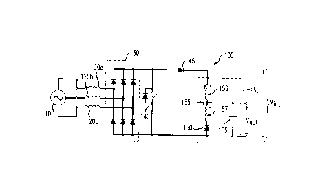
Referring initially to FIGURE 1, illustrated is a
schematic diagram of an embodiment of a three phase boost
converter 100 constructed according to the principles of
the present invention. The boost converter 100 receives
input power from a three-phase voltage source 110 through
first, second and third boost inductors 120a, 120b, 120c
that are coupled to a rectifier 130 comprising a
plurality of diodes arrayed in a full bridge
configuration. The rectifier 130 rectifies the AC input
voltage prior to its delivery to the boost converter's
100 output stage when a boost switch 140 is OFF, i.e.,
not conducting. When the boost switch 140 (illustrated
with an internal body diode) is ON, i.e., conducting, the
boost diode 145 becomes reverse biased, thus isolating
the output stage. Also, during the period when the boost
switch 140 is ON, the AC input supplies energy to the
first, second and third boost inductors 120a, 120b, 120c.
As discussed previously, at the beginning of each
switching cycle when the boost switch 140 is ON, currents
through the first, second and third boost inductors 120a,
120b, 120c [when operating in discontinuous current mode
(DCM)] begin to ramp up from an initial value of zero at
a rate that is proportional to the boost inductors
corresponding phase to neutral voltage. Consequently,
the boost inductor currents, which are also the phase
currents, are naturally proportional to their
corresponding phase voltage during the period when the
CA 02267723 1999-03-24
boost switch 140 is ON. When the boost switch 140 is
OFF, an output voltage Vboost that is higher than the
peak of the input phase-to-phase voltage will drive the
first, second and third boost inductors' 120a, 120b, 120c
currents to reduce back to zero prior to the initiation
of the next switching cycle. The rate of decrease of
each inductor's current, however, is not proportional to
its corresponding input phase-to-neutral voltage due to
the different amounts of energy that had been stored in
each inductor. Consequently, the inductor currents
during the period when the boost switch 140 is OFF are
also not proportional to the inductors' corresponding
phase-to-neutral voltage resulting in distortions in the
input phase currents. It should be noted that the higher
the output voltage Vboost is, the faster are the
individual inductor current's rate of decrease. The
faster the inductor currents are decreased to zero has
the corresponding benefit of reducing the distortions in
the input currents.
Studies have shown that to achieve a total harmonic
distortion (THD) of less than 10~, the output voltage is
required to be greater than 1.7 times the input phase-to-
phase peak voltage (M > 1.7; where M = Vout/Vin(rms)).
This high output voltage requirement for a low THD
normally results in an output voltage that is higher than
what is generally desired. For example, for an input
voltage 208 Vrms and taking into account the presence of
input voltage fluctuations, the output voltage would be
required to be about 650 V to realize THDs of less than
100. This 650 V output voltage is much higher than a 440
V output that is normally desired. For an input voltage
of 440 Vrms, the required output voltage would then have
to be as high as 1300 V (far above a conventional 800 V
CA 02267723 1999-03-24
g
output) to achieve THDs of less than 10~.
The present invention discloses a novel circuit that
takes advantage of the low THD inherent in a boost
converter with high M, e.g., M > 1.7. The present
invention introduces a circuit at the output stage of the
boost converter 100 that provides an output voltage Vout2
that is at a desired lower value while still enjoying the
low THD provided by the boost operation.
At the output stage of the boost converter 100, an
output circuit 150 is shown coupled to the boost diode
140. The output circuit includes an autotransformer 155
that is coupled to a diode 160. Those skilled in the art
should readily appreciate that an active switch may be
substituted for the diode 160 in other advantageous
embodiments. The output voltage Vout2 is derived from an
intermediate tap of the autotransformer 155. In the
illustrated embodiment, the intermediate tap is the
center tap of the autotransformer. It should be noted
that in other advantageous embodiments, the intermediate
tap may not "bisect" the windings of the autotransformer.
An output capacitor 165 is shown coupled across the
intermediate tap of the autotransformer 155 and the diode
160 to attenuate DC components in the output voltage
Vout2.
To illustrate the operation of the converter 100,
assume the turns-ratio of the two windings of the
autotransformer 155 are equal, i.e., 1:1, and the output
voltage Vboost is selected to be at a value just slightly
higher than the peak value of the input phase-to-phase
voltage.(which is the minimum possible voltage with any
type of boost converter). V~hen the boost switch 140 is
turned OFF, the output voltage Vboost that is driving the
discharge of the first, second and third inductors 120a,
CA 02267723 1999-03-24
9
120b, 120c is twice the output voltage Vout2 (assuming
negligible voltage drops across the diode 160). The
output voltage Vboost, at twice the value of the output
voltage Vout2, provides a M > 2 value, preserving the low
THD feature of a boost converter with high M values.
Additionally, since the operation of the converter 100 is
equivalent to the operation of a boost converter with M
> 2, the first, second and third inductors' 120a, 120b,
120c charging periods are always greater than their
respective discharging periods (when the autotransformer
155 is in use) that ensures the autotransformer 155
enough reset time during each switching cycle of the
boost switch 140. Although an autotransformer with
turns-ratio of 1:1 has been described, in other
advantageous embodiments, autotransformers with different
turns-ratio may be employed.
The operation of the boost converter 100 may be
improved with the addition of a snubber to clamp the
voltage "overshoot" transients on the boost switch 140,
due to leakage inductances of the autotransformer 155,
when the boost switch 140 is turned OFF . The snubber
reduces the stresses on the boost switch 140 during
switching intervals and transients. Specific embodiments
of snubber circuits that may be advantageously employed
in the converter 100 are illustrated in FIGURES 2 and 3.
The illustrated embodiments of snubber circuits are
conventional snubber circuits well known in the art.
Hence, their operation will hereinafter not be described
in detail. For a better understanding of snubber
circuits and their application in switching power
converters, see "Power Electronics: Converters,
Applications and Design," by Ned Mohan, et al., John
Wiley & Sons, Inc. (1989), which is herein incorporated
CA 02267723 1999-03-24
by reference.
Turning now to FIGURE 2, illustrated is a schematic
diagram of an embodiment of a converter 200 using the
principles of the present invention and further employing
5 an active lossless snubber circuit 210. The active
lossless snubber circuit 210 includes an auxiliary switch
220 series-coupled with a snubber capacitor 230.
Turning now to FIGURE 3, illustrated is a schematic
diagram of an embodiment of a converter 300 using the
10 principles of the present invention and further employing
a passive lossless snubber circuit 310. The passive
lossless snubber circuit 310 includes a capacitor 320
that is series-coupled with an inductor 340 and a diode
350 across a boost switch 360. Also illustrated in the
passive lossless snubber circuit is a diode 330 that is
coupled to the output of the converter 300.
[Yimin, I have not described the operation of the
snubber circuits (I believe they are prior art, if so
provide a reference). If they are not prior art or if
you would like a description of their operation included
in the application, please provide a description of their
operation (a brief description is all that is necessary]
Although the present invention has been described in
detail, those skilled in the art should understand that
they can make various changes, substitutions and
alterations herein without departing from the spirit and
scope of the invention in its broadest form.