Note: Descriptions are shown in the official language in which they were submitted.
CA 02268123 1999-04-14
WO 98/19435 PCT/US97/20171
MICRODISPLAY FOR PORTABLE COMMUNICATION SYSTEM
RELATED APPLICATIONS
This is a continuation-in-part of U.S. Serial No.
08/942,272 filed on September 30, 1997 of Jacobsen, et al.
which is a continuation-in-part application of U.S. Serial
No. 08/884,485 filed on June 27, 1997 of Jacobsen, et al.
which is a continuation-in-part application of U.S. Serial
No. 08/855,909 filed May 14, l997, which is a continuation-
in-part application of U.S. Serial No.08/853,630 filed on
May 9, 1997 of Jacobsen, et. al. which is a continuation-
in-part application of U.S. Serial No. 08/838,420 filed on
April 7, 1997 of Jacobsen, et. al. which is a
continuation-in-part application of U.S. Serial No.
08/810,646 filed on March 3, l997, which is a Continuation-
in-Part application of U.S. Serial No. 08/766,607 filed on
December 13, 1996 which is a continuation-in-part
application of U.S. Serial No. 08/741,671 filed on October
31, 1996, the entire contents of the above applications
being incorporated herein by reference.
BACKGROUND OF THE INVENTION
Flat-panel displays are being developed which utilize
liquid crystals or electroluminescent materials to produce
high quality images. These displays are expected to
supplant cathode ray tube (CRT) technology and provide a
more highly defined television picture or computer monitor
image. The most promising route to large scale high
SUBSTITUTE SHEET (RULE 26)
CA 02268123 1999-04-14
WO 98/19435 PCT/US97/20171
-2-
quality liquid crystal displays (LCDs), for example, is the
active-matrix approach in which thin-film transistors
(TFTs) are co-located with LCD pixels. The primary
advantage of the active matrix approach using TFTs is the
elimination of cross-talk between pixels, and the excellent
grey scale that can be attained with TFT-compatible LCDs.
Flat panel displays employing LCDs generally include
five different layers: a white light source, a first
polarizing filter that is mounted on one side of a circuit
panel on which the TFTs are arrayed to form pixels, a
filter plate containing at least three primary colors
arranged into pixels, and finally a second polarizing
filter. A volume between the circuit panel and the filter
plate is filled with a liquid crystal material. This
material will allow transmission of light in the material
when an electric field is applied across the material
between the circuit panel and a ground affixed to the
filter plate. Thus, when a particular pixel of the display
is turned on by the TFTs, the liquid crystal material
rotates polarized light being transmitted through the
material so that the light will pass through the second
polarizing filter.
The primary approach to TFT formation over the large
areas required for flat panel displays has involved the use
of amorphous silicon, which has previously been developed
for large-area photovoltaic devices. Although the TFT
approach has proven to be feasible, the use of amorphous
silicon compromises certain aspects of the panel
performance. For example, amorphous silicon TFTs lack the
frequency response needed for high performance displays due
to the low electron mobility inherent in amorphous
mate~~ial. Thus the use of amorphous silicon limits display
SUBSTITUTE SHEET (RULE 26)
CA 02268123 1999-04-14
WO 98/19435 PCT/US97/20171
-3-
speed, and is also unsuitable for the fast logic needed to
drive the display.
As the display resolution increases, the required
clock rate to drive the pixels also increases. In
addition, the advent of colored displays places additional
speed requirements on the display panel. To produce a
sequential color display, the display panel is triple
scanned, once for each primary color. For example, to
produce color frames at 20 Hz, the active matrix must be
driven at a frequency of 60 Hz. In order to reduce flicker
it is desirable to drive the active matrix at 180 Hz to
produce a 60 Hz color image. At over 60 Hz, visible
flicker is reduced.
Owing to the limitations of amorphous silicon, other
alternative materials include polycrystalline silicon, or
laser recrystallized silicon. These materials are limited
as they use silicon that is already on glass, which
generally restricts further circuit processing to low
temperatures.
Integrated circuits for displays, such as, the above
referred color sequential display, are becoming more and
more complex. For example, the color sequential display is
designed for displaying High Definition Television (HDTV)
formats requiring a 1280-by-1024 pixel array with a pixel
pitch, or the distance between lines connecting adjacent
columns or rows of pixel electrodes, being in the range of
15-55 microns, and fabricated on a single five-inch wafer.
SUMMARY OF THE INVENTION
In accordance with the invention, the cost and
complexity of high resolution displays is significantly
reduced by fabricating multiple integrated displays of
reduced size on a single wafer and then dicing the wafer to
produce a plurality of display devices.
SUBSTITUTE SHEET (RULE 26)
CA 02268123 1999-04-14
WO 98/19435 PCT/US97/20171
-4-
The displays are then assembled with appropriate
magnifying optics to form a portable display system of low
cost and reduced size. Included in the optics is a
magnification system which compensates for the small image
size by magnifying and projecting the image at an
appropriate distance for viewing.
In preferred embodiments, the microdisplay, because of
its small size and weight, can be used as a hand-held
communication system such as a pager, a wireless mobile
telephone, or alternatively) as a head-mounted display,
video camcorder, digital camera or a card reader display
system. The display can provide a visual display suitable
for data, graphics or video and accommodate standard
television or high definition television signals. The
system can optionally include circuitry for cellular
reception and transmission of facsimile communications, can
be voice activated, can include a mouse operated function,
provide Internet access, and can have a keyboard or touch
pad for numeric or alphabetic entry. The system can have,
such as in a card reader display system, a housing with a
port or aperture to receive a card, and a card reader for
reading information from the card and displaying the
information on the micro-display.
The telephone or hand-held unit can be equipped with a
camera or solid state imaging sensor so that images can be
generated and transmitted to a remote location and/or
viewed on the display. Also the telephone user can call to
access a particular computer at a remote location, present
the computer screen on the microdisplay, access specific
files in the computer memory and download data from the
file into a memory within the telephone or a modular memory
and display unit connected to the telephone. The telephone
can be connected to a Local computer or display and the
data from the file can be loaded into the local memory.
SUBSTITUTE SHEET (RULE 26)
CA 02268123 1999-04-14
WO 98/19435 PCT/iJS97/20171
-5-
The video camcorder or digital camera has a
microdisplay for a viewfinder. Either an image as seen
through the lens or as previously recorded can be seen
through the viewfinder, depending on what is selected.
In a preferred embodiment of the invention, a light
emitting diode (LED) device is used to illuminate the
display. For transmission displays the LED device operates
as a backlight and can include a diffuser. An LED device
can also be used as a light source for a reflective display
in another preferred embodiment of the invention. The
displays are preferably liquid crystal displays using a
twisted nematic liquid crystal material. Consequently,
controlling the time domain is not necessary to obtain grey
scale.
For the purposes of this application, a microdisplay
is defined as a display having at least 75,000 pixel
electrodes and an active area of less than 160 mm', where
the active area of the display is the area of the active
matrix circuit that generates an image, including all of
the pixel electrodes but not including the driver
electronics and the border area for bonding and sealing of
the liquid crystal display. For example, the array can be
at least 320 x 240, 640 x 480 or higher. A preferred
embodiment of the microdisplay has an active area of 100mm~-
or less, and is preferably in the range between 5mm~ and
80mm~. The pixel pitch for these displays is in the range
of 5 - 30 microns and preferably in the range between 5 and
18 microns. By utilizing pixel pitches of less than 18
microns smaller high resolution displays are now possible.
For an embodiment utilizing a high definition format such
as 1280 x 1024, and utilizing a pixel pitch of 12 microns
or less, the active area of the display is less than
200mm~'.
SUBSTITUTE SHEET (RULE 26)
CA 02268123 1999-04-14
WO 98/19435 PCT/US97120171
-6-
For displays of this size and resolution to be read by
a user at distances of less than 10 inches (25.4 cm) there
are specific lighting and magnification requirements. For
a 0.25 inch (6.35 mm) diagonal display, for example, the
LED device preferably includes a plurality of ZEDS coupled
to a diffuser. The lens used to magnify the display image
has a field of view in the range of 10 - 60 degrees, and
preferably at least about 16 degrees - 22 degrees, an ERD
in the range of about 25 mm - 100 mm and an object distance
l0 of between about 1.5 and 5 feet (152.4 cm). A color field
sequentially operated LED backlight system can use a
plurality of ZEDS with a two or four sided reflector
assembly to concentrate the light through the liquid
crystal display. A preferred embodiment can use at least
two LEDs, or as many as six or more of each color, to
provide the desired brightness level. Alternatively the
LEDs can be arranged around the periphery of a transmissive
display and directed down into a conical reflector that
directs the backlighting through the display in
concentrated form.
The backlight, the display and the viewing lens can be
aligned along a single axis within a small housing volume
that is less than 20cm', and preferably less than l2cm'.
The system weighs less than 10 grams, preferably in the
range between 5 and 8 grams. The system can be
incorporated into battery operated personal communication
devices without substantial alteration of their form factor
and weight requirements.
While a transmissive microdisplay with a backlight is
preferred, a reflective microdisplay can also be used. The
light from the light source is directed onto the same side
of the display that is viewed by the user. An optical
system directs the reflected image from the pixel
electrodes onto a line of sight of the user. Reflective
SUBSTITUTE SHEET (RULE 2fi)
CA 02268123 1999-04-14
WO 98/19435 PCT/US97/20171
_7_
displays can be used in connection with the portable
communications and display systems described herein.
The display can be operated using a color sequential
system as described in U.S. Patent Application Serial No.
08/216,817, "Color Sequential Display Panels" filed on
March 23, 1994, which issued as U.S. Patent No. 5,642,129,
and of U.S. Patent No. 5,673,059, the entire contents of
these patents being incorporated herein by reference.
These patents disclose an active matrix display in which
the control electronics is integrated with the active
matrix circuitry using single crystal silicon technology.
The control electronics provides compressed video
information to produce a color image for data, a still
image or a video image such as a television image on the
display. The use of LEDs to provide color sequential
operation has a number of advantages. The system provides
a lightweight, low-power light source that generates red,
green and blue color components in sequence. The same
control circuit operates the light source and the display
to pulse the appropriate color elements for each
corresponding display image.
The light source can also be pulsed for monochrome
display applications. The same circuit can be used for
both color sequential and monochrome systems. For
monochrome operation the light source need only be flashed
momentarily to provide the desired brightness level. By
flashing the lamp briefly while a given frame is written on
the display, the display power consumption can be
substantially reduced, the voltage holding requirements of
the display are reduced, and heat loading is reduced. The
vertical synchronization signal can be used to trigger the
light source pulse which need only extend for less than a
third of the time needed to write a particular frame onto
SUBSTITUTE SHEET (RULE 26)
CA 02268123 1999-04-14
WO 98/I9435 PCT/US97/20171
_g_
the display. Two flashes in a frame can also be used to
reduce flicker.
The microdisplays described herein can be used in head
mounted displays, cameras, card readers and portable
communications systems, including color sequential systems
as described in greater detail in U.S. Application Serial
No. 08/410,l24 filed on March 23, l995, the entire contents
of which is incorporated herein by reference. Further
details regarding the drive electronics suitable for a
microdisplay can be found in U.S. Serial No. 08/106,4l6
filed on August 13, 1993, the entire contents of which is
incorporated herein by reference. A preferred embodiment
of the display control circuit utilizes an "under scanning"
feature in which selected pixels are rapidly turned on and
off to enhance edge definition and emulate a higher
resolution display. The display control circuit can also
utilize a panning capability so that a small portion of a
displayed image can be selected, by mouse operation for
example, and presented using the entire microdisplay image
area thereby allowing the user to perceive smaller
displayed features. This can also be used to view selected
portions of a high resolution image, such as a portion of a
640 x 480 image on a 320 x 240 microdisplay.
As is readily apparent from the various embodiments
described, one of the benefits of the microdisplay is the
portability of the device using the microdisplay. An
inherent concern with portability is providing enough power
to operate the device for extended periods. One of the
features of a preferred embodiment is the alternating of
the voltage on the counterelectrode, therein allowing the
microdisplay to operate at a lower voltage and therefore at
a reduced power level. Another feature of a preferred
embodiment is stopping the clock to the display when the
SUBSTITUTE SHEET (RULE 26)
CA 02268123 1999-04-14
WO 98/19435 PCT/US97/20171
_g_
display is not being written to, therein reducing power
consumption.
When the display is used to display text, wherein the
image display is not constantly changing, a feature of the
preferred embodiment is to reduce the frame rate, or
refresh rate. The reduction in frame rate results in a
decrease in power consumption.
An additional problem with portability is the
increased likelihood that the device will be used in non-
l0 ideal conditions. One such variable is the temperature in
which the device will operate as temperature affects the
performance of liquid crystal material. One of the
features of a preferred embodiment is the monitoring of the
temperature of the liquid crystal and the integral heating
of the device.
BRIEF DESCRIPTION OF THE DRAWINGS
The above and other objects and features of the
invention will be better understood and appreciated by
those skilled in the art in view of the description of the
preferred embodiments given below in conjunction with the
accompanying drawings, in which:
Figure 1 is a perspective view of a single wafer
having a plurality of display devices formed thereon in
accordance with the invention.
Figure 2A is a schematic illustration of a die for an
integrated active matrix panel display which includes
optional control signal circuitry therein.
Figure 2B and 2C illustrate preferred embodiments of
display control circuits in accordance with the invention.
Figure 2D illustrates a method for selectively
displaying an image on a display in accordance with the
invention.
SUBSTITUTE SHEET (RULE 26)
CA 02268123 1999-04-14
WO 98/19435 PCT/US97120171
-10-
Figure 2E illustrates a timing diagram for the display
control circuit illustrated in Figure 2D.
Figure 2F illustrates an alternative preferred
embodiment of the display control circuit in accordance
with the invention.
Figure 2G illustrates a timing diagram for the display
control circuit illustrated in Figure 2F
- Figure 2H illustrates a portion of the display control
circuit shown in Figure 2F.
Figure 2I illustrates an alternative timing diagram
for the display control circuit illustrated in 2F.
Figure 2J illustrates an alternative preferred
embodiment of the display with a heat gate.
Figure 2K illustrates a portion of the display shown
in Figure 2J.
Figure 2L illustrates an alternative embodiment of a
portion of the display shown in Figure 2J.
Figure 2M is an enlarged sectional view of the display
in its housing.
Figures 3A and 3B are exploded views of a video
display device and pager in accordance with a preferred
embodiment of the invention.
Figures 4A-4K are exterior views of hand-held imaging
devices in accordance with the invention.
Figure 4Ba is a partial cross section rear view of a
preferred embodiment of a pager with integrated camera in
accordance with the invention.
Figure 4L is a functional block diagram of a preferred
pager according to the invention.
Figure 5A is a side view of a lens suitable for
magnifying a microdisplay in accordance with the invention.
Figure 5B is a side view of a multi element lens
providing an increased field of view.
SUBSTITUTE SHEET (RULE 26)
CA 02268123 1999-04-14
WO 98/19435 PCT/US97/20171
-11-
Figure 5C is a cross-sectional view of a display
assembly with a fixed lens.
Figure 5D is a schematic view of an LED backlighting
system for a liquid crystal display in accordance with the
invention.
_ Figures 5E - 5P illustrate additional preferred
embodiments of a backlighting system in accordance with the
invention.
Figure 5Q illustrates a single lens positioned
adjacent the kinoform.
Figure 5R illustrates the first three zones of a
kinoform.
Figure 6A is an optical diagram of a lighting system
for a reflective liquid crystal display.
Figure 6B is an enlarged sectional view of a
reflective liquid crystal display in its housing.
Figure 6C is an enlarged sectional view of a
reflective liquid crystal display with an alternative
backlight.
Figures 7A-7G illustrate preferred LED backlighting
systems for a transmission type display.
Figure 8A is a perspective view of a preferred
embodiment mobile telephone having a display device in
accordance with the invention.
Figures 8B-8C illustrate an alternative embodiment of
a mobile telephone having a display device in accordance
with the invention.
Figures 8D-8G illustrate the changing of the
resolution of the display from high resolutions to low
resolutions.
Figures 8H-8I illustrate an alternative embodiment of
a mobile telephone having a display device in accordance
with the invention.
SUBSTITUTE SHEET (RULE 26)
CA 02268123 1999-04-14
WO 98/19435 PCT/CTS97/20171
-12-
Figures 9A-9J are illustrations of further preferred
embodiments of a telephone microdisplay system in
accordance with the invention.
Figures 10A and 10B illustrate another preferred
embodiment of a telephone microdisplay system.
Figure 11 illustrates another preferred embodiment of
a telephone microdisplay system in accordance with the
invention.
Figures 12A and 12B illustrate rear views of another
preferred embodiment of a telephone microdisplay.
Figures 13A-13K illustrate other preferred embodiments
of the invention including a display docking system for a
cellular telephone.
Figures 13L-13N illustrate a folding keyboard with a
touchpad for uses with phone, display docking system, or
pager.
Figures 13O-13S illustrate other preferred embodiments
of the invention including a display docking system for a
cellular telephone.
Figure 13T illustrates an alternative embodiment of a
display control circuit for a telephone or docking station
capable of receiving an analog phone or a digital phone.
Figure 13U illustrates another preferred embodiment of
the docking station shown in Figures 13Q-135.
Figures 13V-13W illustrate another preferred
embodiment of a display docking system.
Figure 13X is a functional block diagram of a
preferred docking station with cellular telephone according
to the invention.
Figures 1~A-14C illustrates the use of a microdisplay
rear projection. system for a telephone video conferencing
station.
SUBSTITUTE SHEET (RULE 26)
CA 02268123 1999-04-14
WO 98/19435 PCTlUS97/20171
-13-
Figures 15A-C are side cross-sectional, front, and
front cross-sectional views of a hand held rear projection
display system in accordance with the invention.
- Figures 16A-16B illustrate a body worn, hand operated
display system in accordance with the invention.
Figures 16C-16D illustrate the use of a microdisplay
as a viewfinder for a camcorder in another preferred
embodiment of the invention.
Figures 16E-16F illustrate the use of a microdisplay
as a viewfinder for a digital still camera in another
preferred embodiment of the invention.
Figure 16G illustrates a display control circuit for a
camera.
Figures 16H and 16I illustrate cameras with moving
mirrors for through the lens viewing.
Figures 16J and 16K illustrate a camera/imager with a
microdisplay as a viewfinder.
Figures 17A-17C illustrate the use of a microdisplay
in a card reader system in accordance with another
preferred embodiment of the invention.
Figure 18 is a schematic circuit diagram for a
portable card reader system.
Figure 19A illustrates another preferred embodiment of
a card reader system.
Figure 19B shows another preferred embodiment of a
card reader system.
Figures 19C-l9Cb is a schematic circuit diagram of a
memory card for a card reader or imager.
Figures 19D, l9Ea and l9Eb is a schematic circuit
diagram of the controller within the reader or imager
Figure 19F is a schematic circuit diagram of an
alternative embodiment of a switcher in the controller.
Figure 20A is a perspective view of a head-mounted
display system of the invention.
SUBSTITUTE SHEET (RULE 26)
CA 02268123 1999-04-14
WO 98/19435 PCT/LTS97/20171
-14-
Figure 20B is a partial schematic perspective view of
the system of Figure 20A emphasizing additional features of
the invention.
Figure 20C is a schematic perspective view of the
system of Figure 20A which emphasizes certain aspects of
the invention.
Figure 20D is a schematic perspective view of the
headband and pads of Figure 20C.
Figure 20E is a partial schematic side view of the
system of Figure 20A.
DETAILED DESCRIPTION OF THE INVENTION
HIGH RESOLUTION ACTIVE MATRIX MICRODISPLAY
A preferred embodiment of the invention utilizes a
process of making a plurality of flat panel displays 10 in
which a large number of active matrix arrays 14 are
fabricated on a single wafer 12 as illustrated in
connection with Figure 1. The number of displays
fabricated on a single wafer depends upon the size of the
wafer and the size of each display. A preferred embodiment
of the invention, for example, uses a high resolution
display having an imaging area of the display with a
diagonal of 0.5 inches (12.7 mm) or less. For a four inch
wafer, forty separate displays can be fabricated on a
single four inch wafer. Where each display has a diagonal
of about 0.25 inches (6.35 mm), 80 displays can be
fabricated on a single wafer, over l20 displays can be
fabricated on a five inch wafer, over l80 displays on a six
inch wafer, and 400 displays can be fabricated on an 8 inch
wafer.
By fabricating a large number of small high resolution
displays on a single wafer the manufacturing yield can be
SUBSTITUTE SHEET (RULE 26)
CA 02268123 1999-04-14
WO 98/19435 PCT/US97/20171
-15-
substantially increased and the cost per display can be
substantially reduced.
To obtain monochrome resolutions of at least 75,000
pixels (e.g. a 320 x 240 array) suitable for displaying an
NTSC television signal on a 0.25 inch diagonal display the
pixel electrodes are preferably on the order of about 15
microns in width or less. To obtain a monochrome
resolution of at least 300,000 pixels (e.g. 640 x 480
array) on a 0.25 inch diagonal display the pixel electrodes
preferably have a width of about 8-10 microns.
These small high resolution displays require
magnification such that when held in a user's hand within
the range of 0.5 inches to 10 inches of the user's eye, a
clear image is provided.
Referring now to Figure 2A, an integrated circuit
active matrix display die is shown schematically which has
been diced from a single wafer along with selected number
of replicated circuits. Incorporated into the circuit 100
are scanner circuits 42a, 42b, 42c, 42d, along with pixel
driven circuits 44a, 44b, 44c, 44d, select scanner circuits
46a, 46b and a display matrix circuit 90.
Further details regarding the fabrication of each die
on a wafer can use the methods described in U.S. Patent
No. 5,256,562, the contents of which incorporated herein
its entirety by reference. Additional details regarding
the fabrication of the active matrix and use within
communication systems is described in U.S. Patent
Application Serial No. , filed October 31, 1997
of Matthew Zavracky and titled "Color Display with Thin Gap
Liquid Crystal" the contents of which is incorporated
herein in its entirety by reference.
By fabricating a selected number of circuits 100 on a
single wafer, the circuit yield from a single wafer is
greatly enhanced at the expense of reduced display area.
SUBSTITUTE SHEET (RULE 26)
CA 02268123 1999-04-14
WO 98/19435 PCT/US97/20171
-16-
However, this area disadvantage i~ overcome by magnifying
and projecting the display image as will be described
herein.
A video signal bus 35-1 through 35-16 carries analog
video signals from digital to analog amplifiers (not shown)
to column drivers 44a-d. Because signal interference and
signal loss can occur as the analog video signal cross each
signal line in the signal bus 35, the channels of video
signals are arranged to reduce interference. As
illustrated, there are four column drivers 44a-44d, two
column drivers 44a,44b at the top of the active matrix
circuit 90 and two column drivers 44c,44d at the bottom of
the active matrix circuit region 90. Each channel is
allocated to one of the column drivers 44 such that each
column driver 44 receives video from four channels. The
top column drivers 44a,44b receive video from the channels
that drive the odd-numbered pixel columns and the bottom
column drivers 44c,44d receive video from the channels that
drive the even-numbered columns. As shown, no video signal
has to cross the path of more than one other video signal.
The illustrated arrangement of column drivers is
particularly suited for edge-to-center and center-to-edge
video writing, although the data can also be written from
left-to-right or right-to-left. It should be understood
that more or less than four column drivers 44 can be
employed in preferred embodiments of the invention. For
applications having resolutions of 320 x 240 or 640 x 480
it is desirable to use single column and row drivers to
drive the display. For high speed, high definition
displays more can be used to improve performance.
The data scanners 42 a-d are responsive to a pixel
data signal 142 and a pixel clock signal 143 from a control
signal generator (not shown). The data scanners 42a-d can
use a shift register array to store data for each scan. An
SUBSTITUTE SHEET (RULE 26)
CA 02268123 1999-04-14
WO 98l19435 PCT/L1S97/20171
-17-
odd shift register array can be used to store data to odd
column pixels and an even shift register array can be used
to store data to even column pixels. As illustrated, there
are left and right odd data scanners 42a,42b and left and
right even data scanners 42c,42d.
The column drivers 44 selected by the data scanner 42
transmit video data to a selected column of C pixels in the
active matrix circuit 90. The select scanner 46 controlled
by a control signal generator determines by control lines
which pixels accept this column data.
To reduce signal loss across the active matrix region
90, the select lines are driven from both sides by select
scanners 46a and b. As viewed in Figure 2A, a left select
scanner 46a and right select scanner 46b are connected to
the select data line 146 and the select clock line 147.
A third enabling line 148 can also be used for specific
applications. The left select scanner 46a provides a
select line signal at the end of the select line nearest
the lowest-valued pixel column (Ci) and right select
scanner 46b provides a select line signal at the end of the
select line nearest the highest-valued pixel column (CN).
Thus, an identical select line signal is supplied at both
ends of the select line.
Although static shift registers can be used, the shift
registers of the data scanner 42 and the select scanners 46
are preferably implemented as dynamic shift registers. The
dynamic shift registers rely on capacitor storage without
leakage. However, dynamic shift registers are susceptible
to leakage, especially when they are exposed to light.
Hence, lighshields are needed to protect the scanners 42a
- 42d,46 from exposure to light. Similarly, light shields
are also used to protect the transmission gates 44 and
pixel columns C:-CN.
SUBSTITUTE SHEET (RULE 26)
CA 02268123 1999-04-14
WO 98/19435 PCT/US97/20171
-18-
For further information regarding the input signals to
the circuit 100, reference is made to the above-cited U.S.
patents and applications.
In a preferred embodiment of the invention, the panel
drive circuitry of Figure 2A is fabricated as an integrated
circuit along with the active matrix circuit 90. The
integrated circuitry is preferably fabricated in single
crystal silicon having a silicon-on-insulator (SOI)
structure using the fabrication and transfer procedures
described previously in the aforementioned U.S. Patent No.
5,256,562. By fabricating the row and column drive
circuitry 42a-42d, 44a-44d, 46a, 46b as well as the
scanners in single crystal material along with the active
matrix circuit 90, the size of the display panel is not
constrained by the connecting pins for the various discrete
components. The integrated fabrication also increases the
operating speed of the display relative to displays
constructed from discrete components. Furthermore, the
drive circuitry can be optimized to increase display
performance. For example, it is easier to construct a
small 1280H x 1024V display panel with dual select scanners
through integrated fabrication than it is using discrete
components.
The pixel electrodes in a preferred embodiment are
between 60 and 2S0 microns square. Consequently, a 1280H x
1024V active matrix with the control system can be
fabricated such that there are at least 40 such integrated
circuits on a five inch wafer, for example.
A preferred embodiment of a display control circuit
for a color sequential microdisplay is illustrated in
connection with Figure 2B. The display control circuit l02
receives an analog composite signal 103 such as a
television or VCR video signal at converter 105. Converter
105 can be a commercially available chip, such as the Sony
SUBSTITUTE SHEET (RULE 26)
CA 02268123 1999-04-14
WO 98I19435 PCT/US97/20171
-19-
CXA1585, which separates the signal 103 into red, green and
blue components. The three analog color components are
converted into digital signals by three respective analog
to digital (A/D) converters 106. The three color digital
signals are stored in red 107, green 108, and blue 109
memory circuits. Circuits 107, l08 and 109 can be RAM,
such as DRAM, frame buffers that are connected to the
timing circuit 110. Timing circuit 110 can be connected to
the converter 105 by an interface bus and receives
horizontal and vertical synchronization signals along lines
119 from converter 105. Circuit 110 controls the
sequential flow of each color frame onto the display by
sending video data from each memory 10I, 108, l09 onto the
display and coordinating actuation of the backlight 111
along lines 115 for each primary color. Lines 114 provide
control of hue and contrast of the resulting image. Lines
116, 117 and 118 are used to control the row and column
driver circuits within display circuit 112. Lines 1l6 and
117 control horizontal shift and vertical shift of the data
as it is read onto the display.
Lines 116 and 117 can be used to allow the user to
invert (i.e. reverse left to right or right to left) the
image on the display. This can be useful for the telephone
user who may select one hand to hold the telephone during
use and simply press a button on the housing so that the
image is inverted for presentation to the eye of the user
when electing to hold the telephone speaker in the other
hand adjacent to the user's ear. The inverting of the image
can be accomplished by several different techniques
including by software and hardware methods. One such
method is to use a bi-directional shift register and shift
the direction of the register to invert the image. Another
technique is to change the method by which the data is
pulled out of memory using the software.
SUBSTITUTE SHEET (RULE 26)
CA 02268123 1999-04-14
WO 98I19435 PCT/L1S97/20171
-20-
Lines 118 control vertical and horizontal pulse,
vertical and horizontal clock, even and odd row enable
signals and the horizontal multiplying pulse signal.
Digital to analog converters 1l3, memories 107, 108, 109,
converter 105 and control circuit 110 can be mounted on a
common circuit board with display 112, or they can be split
onto separate circuit boards or integrated circuits within
the telephone housing, the pager housing, the docking
element housing, or other housing described in greater
detail below depending on the geometry and operational
requirements of the specific embodiment. In addition to
placing the digital to analog converters, memories,
converter and control circuit 110 on a common circuit
board, they can be all located on a single monolithic
integrated circuit (IC), represented by a dash line l01.
The placing of a components on a single IC reduces the
internal capacitance and therefore the power consumption of
the circuit.
Another preferred embodiment of a display control
circuit is illustrated in connection with Figure 2C. In
this embodiment, a digital circuit 120 is used to control
color sequential display operation. The processor 134
receives serial digital image data at 121 and sends display
data to memory l24. An optional additional non-volatile,
such as flash memory or SRAM circuit 125 can also be
included to store graphics data where that is in addition
to text stored at 124 using a serial bus 127. Timing
control circuit Z22 receives clock and digital control
signals from processor 134 and transmits control signals to
the backlight Ill and display 1l2 along lines 11S, 116,
117, and l18, respectively. Lines l28 direct ready, reset,
write enable, output enable, color enable, address and data
signals to memory to control deliver of image frames to the
display 112. This circuit can be used within a telephone
SUBSTITUTE SHEET (RULE 26)
CA 02268123 1999-04-14
WO 98/I9435 PCT/US97/20171
-21-
housing or the docking element housing described in greater
detail below depending on the geometry and operational
requirements of the specific embodiment. A switch can be
provided to allow the user to reverse the image on the
display left to right or right to left. This can be
useful for the telephone user who may select one hand to
hold the telephone during use and simply press a button on
the housing so that the image is inverted for presentation
to the other eye of the user when electing to hold the
telephone speaker in the other hand adjacent to the user's
other ear.
Power management circuit l23 receives control signals
along line 126 from circuit 122 to lower power consumption
of the circuit 120. Circuit 123 is used to control power
during display operation, and is connected to flash memory
circuit 125, the digital to analog converter, the
buffer/inverter and the display 112 by a line 129. This
capability arises from the use of a transferred thin film
active matrix circuit described previously which has an
ability to store charge between vertical synchronization
pulses. This storage capacity enables lower power
consumption of the display and backlight at less than 0.2
Watts. Thus, after a frame of data is written on the
display, power is lowered until the next frame is written.
This lengthens battery cycle time of portable communication
devices as described herein. The power can be lowered by
periodically stopping the clock to the display as described
below.
Figure 2D illustrates a method of displaying
information cn the display in which large amounts of
information are contained in each image. For such high
information images it may be desirable to enlarge a
selectable portion of that image on the display. For
example, the full image 130 has a region 131 in which a
SUBSTITUTE SHEET (RULE 26)
CA 02268123 1999-04-14
WO 98/I9435 PCT/US97/20171
-22-
cursor 133 can be positioned. The user can position the
cursor using a mouse or button control element anywhere
within region 131 and identify a subregion 132. The user
selects the image of subregion for display on the full
display area.
If the data provided by the processor 134 is greater
than that displayed on the display 112, the image can be
written to the display by underscanning; e.g. only every
fourth bit of display is written. In order to display the
image of a subregion as the entire image, every bit of
display is written, but only for that specific region. If
the subregion 132 is to be displayed on the full display
area, the data for the rows above subregion 132 are not
forwarded to the display 1I2 by the timing control circuit
I22, and only the columns that are included in subregion
132 are forwarded.
Figure 2E illustrates a timing diagram that
illustrates a preferred method of operating a microdisplay
in accordance with the invention. The video signal is sent
to the display 1l2 both as actual video and inverted video.
The odd-numbered pixel columns receive video from the top
column driver and the even-numbered columns receive video
from the bottom column driver as described above with
Reference to Figure 2A. Referring to the embodiment of
Figure 2E, the odd-numbered pixels, which receive actual
video, are driven between the common voltage (V~oM), the
voltage applied to the counterelectrode, and the supply
voltage source (Vp~). The even-numbered pixels, which
receive the inverted video, are driven between V~o,: and the
supply voltage sink (VEE). After the entire frame is
scanned into the display and there is a delay to allow the
liquia crystal to twist, the backlight is flashed to
present the image. In a preferred embodiment, Vpp is 9
volts, V.- is 2 volts and V~oM is 5.5 volts. The technique
SUBSTITUTE SHEET (RULE 26)
CA 02268123 1999-04-14
WO 98/19435 PCT/US97/20171
-23-
of alternating the video on each column is called column
inversion and helps prevent a DC voltage from building up
on the liquid crystal material and additionally prevents
cross talk.
Another preferred embodiment of a display control
circuit is illustrated in connection with Figure 2F. In
this embodiment, a digital circuit 1120 is used to control
color sequential display operation as described in relation
to Figure 2C. Additionally, the circuit has the features
of a modulating common voltage and a heater, as described
below. The processor 1104 receives image data at 1121 and
sends display data to memory 1124 and flash memory 1125 via
the timing control circuit 1122. The image data can be in
a variety of forms including serial or parallel digital
data, analog RGB data, composite data or s-video. The
processor 1104 is configured for the type of image data
received, as is well known in the art. The timing control
circuit 1122 receives clock and digital control signals
from the processor 1104 and transmits control signals to
the backlight 1111 along lines l115. The timing control
circuit 1l22 transmits control signals, such as vertical
start pulse, vertical clock, horizontal start pulse, and
horizontal clock, to the display 1112 along lines l116,
l117, and 1118. Lines 1128 direct ready, reset, write
enable, output enable, color enable, address and data
signals to memory to control delivery of image frames to
the display 1112.
Still referring to Figure 2F, the image data travels
from the timing control circuit 1l22 to the display I112
through a digital to analog converter l130 and through an
inverter 1131 on an alternate frame dependent on a switch
1132 as described below. In addition and in contrast to
previous embodiments, the common voltage (V~~,s)enters the
display 1112 at alternating values controlled by a switch
SUBSTITUTE SHEET (RULE 26j
CA 02268123 1999-04-14
WO 98I19435 PCT/US97/20171
-24-
1133. The switches 1133 and 1132 for alternating the V~oM
and the video to the display are controlled by a frame
control line l134 from the timing control circuit 1122.
Referring to Figures 2G and 2F, with the common
voltage (V~oM)high, approximately 3 - S volts in a preferred
embodiment, the actual video signal is scanned into the
matrix circuit. After a delay to allow for the liquid
crystal to twist to maximum position, the LED backlight
1111 is flashed to present the image. Prior to the next
frame, frame 2 in Figure 2G, Voor: goes low, approximately
zero (0) volts in a preferred embodiment. Driving Voo,., low
erases the image that has just been scanned. However,
since there is no backlight on, the loss of the image is
not seen. With V~oM low, the inverted video signal is
scanned into the matrix circuit. Similarly, after a delay
to allow the liquid crystal to twist, the LED backlight
1111 is flashed to present the refreshed or new image.
Prior to the next frame, frame 3 in the Figure, Voo~ goes
high. Driving VooM high results in the image that has just
been scanned to be erased. With VooM high, an actual video
signal is scanned into the matrix circuit. A delay occurs
and then the LED backlight 1111 is flashed. The common
voltage (V~o~,) and the video keep on alternating. If the
display is a color display, the LED backlight l111
sequentially flashes the distinct colors. In addition,
three screen scans, one for each color LED, comprises a
frame and the V~or, alternates each screen.
In a preferred embodiment, V~oM fluctuates every 15-20
milliseconds. It takes 3-5 milliseconds to writejscan the
image. The LED flashes for a time period of about 3
milliseconds. It is recognized that it may be desirable to
vary the delay time before flashing the LED or varying the
length of the LED flash dependent on the color LED to be
flashed. For example, it may be desirable to have a longer
SUBSTITUTE SHEET (RULE 26)
CA 02268123 1999-04-14
WO 98/19435 PCT/iJS97/20171
-25-
delay time, response time, before flashing the LED when the
LED to be flashed has a longer wavelength, such as red,
which has a wavelength of between 630 and 700 nm.
With the video amplitude, the difference between Vpp
and VET, on the pixel's TFT reduced, a smaller storage
_ capacitor is required. Less time is need to write with a
smaller storage capacitor and therefore a smaller pixel TFT
can be used. If the liquid crystal has a fast enough
response, the storage capacitor can be eliminated and the
capacitance of the liquid crystal becomes the storage
capacitor. In addition, with no storage capacitor a larger
aperture is possible. With larger aperture and increased
aperture ratio, the image will be brighter for the same
cycling of the backlight or the total power used can be
reduced with the same image brightness.
Referring to Figure 2H, an enlarged schematic view of
one pixel, the pixel is charged by the horizontal shift
register 1136 selecting a column 1138 by turning a
transmission gate 1140 and the vertical shift register 1142
selecting a row 1144. The video is written to the pixel
and the liquid crystal begins to twist and become optically
transmissive. After the entire display has been written
and there has been a delay before the LED flashes, the V~o,.,
1146, i.e., the voltage to the counterelectrode, is
switched from high to low or vice versa by the frame
control line. At the same time, the video signal is
switched from actual video to inverted video or vice versa,
so that the video will be switched for the next frame.
The liquid crystal can be twisted to become either
optically transmissive or optically opaque. The
orientation of the polarizers affect whether the liquid
crystal is driven to white, transmissive, or to dark)
opaque.
SUBSTITUTE SHEET (RULE 26)
CA 02268123 1999-04-14
WO 98/19435 PCT/CTS97/20171
-26-
Referring back to Figure 2F, the display circuit has
an additional line, a temperature sensor line 1148, which
runs from the display 1112 to the timing control circuit
1122. The active matrix comprises a plurality of pixels
arranged in columns and rows. Heat is preferably absorbed
substantially uniformly throughout the liquid crystal
material. However, there may be local temperature
variations due to the nature of the image being displayed
as well as display and heater geometry and environmental
conditions. Temperature sensors can be distributed
throughout the active matrix region including around the
perimeter of the active matrix including the corners and
also disposed near the center of the active matrix. The
use of a temperature sensor is described in U.S. Patent
Application Serial No. 08/364,070 filed December 27, 1994
and is incorporated herein by reference.
The characteristics of the liquid crystal material is
effected by the temperature of the liquid crystal. One such
example is the twist time of twisted-nematic liquid crystal
material, which is shorter when the liquid crystal material
is warm. By knowing the temperature of the liquid crystal,
the timing control circuit 1122 can set the duration and
timing of the flash of the backlight 1111, therein
achieving desired brightness and minimizing power
consumption.
The measuring of the temperature of the liquid crystal
requires additional analog circuitry which add complexity
to the circuit of the display. It is recognized that the
temperature of the liquid is related to its capacitance.
Therefore, the capacitance of the liquid crystal, an
electrical measurement, can be done in place of the
measurement of the temperature in order to determine when
heating is required.
SUBSTITUTE SHEET (RULE 26)
CA 02268123 1999-04-14
WO 98/19435 PCT/US97I20171
-27-
Another preferred embodiment of the display 1112 has
an internal heater. Referring back to Figure 2H, during
normal operations, the vertical shift register 1142 has
only one row on, so that as the horizontal shift register
1136 moves from column to column only one pixel is
affected. After the last pixel on a row is addressed, the
vertical shift register 1142 switches the active row. The
display 1112 can be placed in a heat mode where each row
1144 is turned on and has a voltage drop across the row to
create heat. In the embodiment shown in Figure 2H, an end
1158 of each row line is connected to Vpo and the end near
the shift register is driven low thereby creating a voltage
differential across each line. The heat is generated since
P=V2/R, where R is the resistance of the row lines. In
normal operation, only the selected line which contains
pixels to be driven low generate heat, not the entire
display.
Referring to Figure 2I, with the common voltage
(V~oM)high, the actual video signal is scanned into the
matrix circuit. After a delay to allow for the liquid
crystal to twist into position, the LED backlight 1111 is
flashed to present the image. Prior to the next screen or
subframe, a heat cycle occurs where all the row lines are
driven such that there is a voltage differential across the
row. The heating can occur while V~~:: and the video are
being alternated and inverted, respectively, by the frame
control line 1131. Figure 2I shows a heating cycle after
each subframe, but the number and time period of heat
cycles can be dependent on the temperature of the liquid
crystal as determined by the temperature sensor 1132. In
cold environments, the digital circuit 1120 can have a
warm-up cycle where the heater is turned on prior to the
first painting of the screen.
SUBSTITUTE SHEET (RULE 26)
CA 02268123 1999-04-14
WO 98I19435 PCT/US97/20171
-28-
Still referring to Figure 2I, driving V~oM low erases
the image that has just been scanned. However, since there
is no backlight on, the erasure of the image is not seen.
With V~oM low, the inverted video signal is scanned into the
matrix circuit. Similarly after a delay to allow the
liquid crystal to twist, the LED backlight 1111 is flashed
to present the refreshed or new image. Prior to the next
screen, frame 1, subframe 3 in the Figure, V~oM goes high.
The driving V~~~., high results in the image that has just
been scanned to be destroyed. With V~oM high, an actual
video signal is scanned into the matrix circuit. A delay
occurs and then the LED backlight 1l11 is flashed. The
common voltage (V~o,.,) and the video keep on alternating.
The delay time before beginning the flash and the
flash time are shown as identical in Figure 2I. However,
both the delay time (the delay for response time of the
liquid crystal) and the flash time can be dependent on the
specific color to be flashed. The delay time is dependent
on when the liquid crystal associated with the last pixel
to be written has sufficient time to twist to allow that
specific color to be seen. The duration of the flash, or
the point that the flash must be terminated, is dependent
on when the liquid crystal associated with the first pixel
to be written of the next frame has twisted sufficiently
that light from the backlight is visible to the viewer.
For example referring to Figure 2I, it is not desirable for
the red flash to be on, when the writing for the blue
subframe has progressed to the point that the first pixel
written for the blue subframe has resulted in the liquid
crystal being optically transmissive for red wavelengths.
The ending of the flash does not have to occur until
sometime after the beginning of the writing of the next
subframe because of response time of the liquid crystal.
SUBSTITUTE SHEET (RULE 26)
CA 02268123 1999-04-14
WO 98I19435 PCT/US97/20I71
-29-
The timing control circuit 1122, as seen in Figure 2F,
can vary the flash duration and the delay or response time
dependent on the color that is to be flashed. In addition,
the current to the backlights 1111 can be varied to adjust
the intensity of the color. If desired, a color control
line 1127 can be added to the timing control circuit 1122
to allow the user to vary the color.
It is recognized that the method of generating heat is
different on different displays. For example, referring to
Figure 2A in which a select scanner 46a and 46b is located
on both sides of the display and is connected to each end
of the row, in typical operations either both ends are high
or both ends are low depending on whether the row is being
addressed. In order to heat the display, one of the select
scanners, for example 46a, can be driven high for all the
rows, and the other select scanner, for example 46b, is
driven low for all rows therein creating a voltage
difference across the row lines.
The clock timing sent to the display 1112 is shown in
Figure 2I. The clock timing is needed by the display 1112
only when writing to the pixels. The capacitance of the
storage capacitor holds the liquid crystal in the proper
position during the time the backlight l111 is flashing.
By periodically sending clock signals to the display 1112
for typically as much as fifty percent (500) of the total
time or less results in a power reduction.
Referring to Figure 2J, a schematic of the display
1l12 and the digital to analog converter l130 are shown.
The display has a horizontal shift register l136, a
vertical shift register 1142, and switches l140 similar to
what is illustrated in Figure 2H. In addition, and in
contrast to Figure 2H, Figure 2J illustrates a heating gate
1l54.
SUBSTITUTE SHEET (RULE 26)
CA 02268123 1999-04-14
WO 98/19435 PCT/LTS97/20171
-30-
Referring to Figure 2K, for pixels which have p-
channel TFTs, the heating gate 1154 has a series of n-
channel TFTs. Typically when writing to the display only
the row being written to is on (V=0). When not writing to
the display, all the rows are VoD. When the n-channel TFTs
turned on, by applying VDO to a heat line 1150 results in
current flowing from the inverter associated with the
vertical shift register 1142 through the row to the n-
channel TFT and heat is dissipated along the entire row.
The drain is connected to VFW,, which is zero. It is also
recognize that the display 1112 can have several extra rows
outside the typical array to assist in uniform heating.
Likewise for pixels which have n-channel TFTs,
referring to Figure 2L the heating gate 1154 has a series
of p-channel TFTs. Typically when writing to the display
only the row being written to is on (V=Vpo). When not
writing to the display, all the rows are approximately zero
(0) volts. When the p-channel TFTs are turned, by setting
the gate to zero (0), there is a voltage drop across the
2 0 row o f Vo~ .
It is recognized that Voo~ addressing and the heating
of the display can used independently. Heating can be
incorporated into the embodiments described with respect to
Figures 2A-2D. While an internal heater is preferred, it
is recognized that a separate heater can be used with the
temperature sensor.
Referring to Figure 2M, a sectional view of the
display 1112 is shown. The display 1112 has an active
matrix portion 1160 including a pixel element 2047 spaced
from a counterelectrode 2085 by an interposed liquid
crystal material 2080. Each pixel element 2047 has a
transistor 2054 and a pixel electrode 206S. The active
matrix portion 1160 can have aluminum light shields 2086 to
protect the transistor (TFT) 2054 if the active matrix is
SUBSTITUTE SHEET (RULE 26)
CA 02268123 1999-04-14
WO 98/19435 PCT/US97/20171
-31-
used for projection requiring high luminance light. The
counterelectrode 2085 is connected to the rest of the
circuit by solder bumps 2088. The matrix 1160 is bounded
by a pair of glass substrates 2090 in this embodiment and a
pair of polarizers 1162. An additional pair of glass
plates l164 are located outboard of the active matrix
portion 1160. The glass plates 1164 are spaced from the
polarizer 1162. The space defines an insulation layer
1166. The display 1112 includes a two-piece case 1l68
which contains the active matrix portion 1160, the glass
plates 1l62 and the polarizers 1164. A room temperature
vulcanization (RTV) rubber 1170 helps in maintaining the
elements in proper position in the case.
Still referring to Figure 2M, an alternative
embodiment for an internal heat is shown. A second layer
of ITO (Indium Tin Oxide) 1174 underlies the
counterelectrode 208S with an interposed layer of Si02
1176. The second layer of ITO 1174 is patterned such that
it covers only the array area. If a current is passed
through the second layer 1l74, it heats and consequently
heats the liquid crystal 2080. Similar to previous
embodiments, the heating occurs between the two layers of
glass 2090 that bound the matrix 1l60.
A preferred embodiment in the form of a stand-alone
video display device 98 featuring a liquid crystal display
incorporating the actual matrix display circuit 100 will
now be described in connection with the exploded views of
Figures 3A and 3B.
In Figure 3A, a portable imaging device such as a
pager is illustrated having a housing including a top 40
and a bottom 43 with a door 50 for access to a battery 48.
The battery 48 provides power to the circuit board 41, the
display 24 and the backlight 22. The pager can be operated
by controls 38 or push buttons accessible through one of
SUBSTITUTE SHEET (RULE 26)
CA 02268123 1999-04-14
WO 98/19435 PCT/US97/20171
-32-
the housing surfaces that actuate display functions. An
optical system 20 is positioned within the housing and
includes a backlight 22, preferably an LED backlight, a
transmission liquid crystal display 24, a focusing
mechanism including a knob 28 that the user rotates to move
the tunnel 30 relative to the optic slide 26, a lens
assembly 32, and a cover glass 34.
Preferred embodiment of hand held display devices are
illustrated in connection with Figures 4A - 4K. Figure 4A
is a perspective view of a preferred embodiment of a pager
system 150 having two display viewing areas 152 and l54
within a housing 155. Viewing area 152 has a lens through
which the user views a microdisplay as described
previously. A second flat panel display without
magnification is viewed by the user at l54. The second
display is a simple low resolution numeric and/or
alphabetic display to read telephone numbers or scrolled
numbers or messages. The microdisplay magnification can be
adjusted at switch 158. The displays are operated by
switches 156, 157. As seen in the rear view of Figure 4B,
the rear surface 162 of housing 155 is thicker in that
portion containing the microdisplay and the battery. In
the alternative embodiment illustrated in Figure 4Ba, the
rear panel 162 is removed to expose the cavity 159 for the
battery and the rear of the display assembly 161. Also
shown in this embodiment is a cover 163 which slides to
cover or expose a camera including an image sensor 166 and
lens 167. The digital imaging sensor l66 can take images
electronically stored within a memory within the pager that
can be sent by wireless transmitter to a personal computer,
a telephone as described herein, or web browser. The
images can also be loaded by wire through port 169 onto a
personal computer, or alternatively, can be loaded onto a
smart card or flash memory card that can be inserted into
SUBSTITUTE SHEET (RULE 26)
CA 02268123 1999-04-14
WO 98!I9435 PCT/ITS97/20171
-33-
one or more card slots 168. The port 169 can also be
connected directly to a keyboard or touchpad as described
herein. The sideview of the housing 155 shown in Figure 4C
illustrates a clip 160 that is used to fasten the device to
the clothing of the user. The clip 160 is attached to the
bottom surface 164 of the housing 15S as shown in Figure
4D.
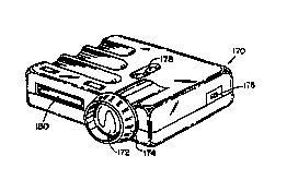
Another preferred embodiment of a hand-held viewing
device 170 is illustrated in the perspective view of Figure
4E. A first display is seen through lens 172 with
magnification being adjusted by knob 174. A second display
l80 as described above is positioned on the same side of
the device 170 as the lens 172 for ease of viewing. The
displays are operated by switch 176 and buttons or control
elements 178. A top view is illustrated in Figure 4F
showing ridges 184 that accommodate the fingers of the user
and the second display switch 182, which is shown more
clearly in the side view of Figure 4G.
Rear and bottom views of device 170 show rear 188 and
bottom 186 sides in Figures 4H and 4I, respectively.
Another preferred embodiment is illustrated in the
perspective views of Figures 4J and 4K. In the embodiment,
a hand held unit 190 has a viewing window 191, a focus
control 192, a rear panel 193 with an external port, a
battery access panel 194, and a control panel 195 with
control elements including a scan control element 196 to
move text or the image on display up or down and left or
right.
An embodiment of the invention is directed to a
wireless communication device 900 such as an enhanced
pager. Figure 4L is a functional block diagram
illustrating such a wireless device. The device 900
includes a processor 902 having read and write access with
memory 904. The processor and other components of the
SUBSTITUTE SHEET (RULE 26)
CA 02268123 1999-04-14
WO 98l19435 PCT/LTS97/20171
-34-
device receive power from a power supply or battery 906
that is preferably light-weight. The processor operates a
transmitter 908 and a receiver 910 to communicate with one
or more base stations 912 within a network, such as a pager
network according to standard wireless communication
protocols. The processor receives commands and data from a
user through input circuitry 914, which can include
switches and scan control elements. The processor provides
information back to the user through output circuitry
including a microdisplay 916 and can also include a
conventional alphanumeric LED or liquid crystal display
918. The pager 900 in addition can have a digital image
sensor 920 for taking images which can be electronically
stored with a memory or loaded onto a smart card or flash
memory card 924 received by a slot 926 in the pager 900.
The pager 900 can also have a port 928 for directly
connecting to an external memory or processor or to, a
keyboard or a touchpad.
A lens 65 suitable for magnifying the image of a
microdisplay for viewing by a user is illustrated in the
example of Figure 5A.
For a 0.25 inch diagonal microdisplay, the outer
diameter 64 of the lens can be about 30.4 mm, the thickness
70 of the lens at the optical axis 67 can be about 8 mm,
the inner surface 60 that receives light from the display
has a curved diameter of about 2l.6 mm, and the viewing
surface 6-~ has a diameter of 68 of about 22.4. The
periphera,~ edge 69 used to hold the lens in the assembly
can have ~ thickness 66 of about 2 mm and a radius 71 of
about 4 mm.. The lens 65 can be made of glass or a plastic
material such as acrylic. This particular example of such
a lens has a 16 degree field of view and an ERD of 25. The
lens assembly can include an automatic focusing system, or
a lens system that collapses in size when not in use.
SUBSTITUTE SHEET (RULE 26)
CA 02268123 1999-04-14
WO 98/19435 PCT/US97/20171
-35-
Another preferred embodiment for providing a color
display can use a diffraction optical system such as those
described in application U.S. Serial No. 08/565,058 filed
on November 30, 1995, the entire contents of which is
incorporated herein by reference.
Another preferred embodiment of a 1.25 inch diameter
lens system 52 with a larger field of view is illustrated
in Figure 5B. Three lens elements 51, 53 and 55 enlarge
the image on the display 54.
The lens 65 of Figure 5A can be used in the
alternative display assembly of 80 of Figure 5C. In this
embodiment, the display 82 is positioned between the
backlight housing 84, containing LED 86, and the lens
housing 88 that holds the lens 65 in a fixed position
relative to the display 82.
A microdisplay system 360 utilizing a folded optical
path is illustrated in connection with Figure 5D. In this
embodiment, an LED array 362, or other light source,
illuminates the display within housing 364. The display
366 directs an image along a first optical path 372 that is
reflected by mirror 368 along a second other path 374
through the lens 370 as described previously.
Another preferred embodiment of the backlight system
is illustrated in Figures 5E-5G. The backlight 375
includes a reflective bowl 376 with an inner concave
surface 382 that reflects light emitted by the LEDs 380
onto the active matrix region of display 377. The LEDs 380
are mounted on a circuit board 378 that is electrically
connected to the timing circuit described previously. The
system 375 can also include a heat sink 379 for
applications requiring thermal isolation of the display
circuit from the backlight circuit. The element 379 can be
a silicon carbide, silicon, or aluminum nickel plate or
wafer. The element 379 can be insulated from the display
SUBSTITUTE SHEET (RULE 26)
CA 02268123 1999-04-14
WO 98/19435 PCT/US97/20171
-36-
377 with layer 381 such as an adhesive. The circuit board
378, element 379 and optional layer 381 have openings that
are aligned to provide an aperture 383.
A preferred embodiment of printed circuit board 378 on
which the LEDs are mounted is shown in Figure 5F. In this
embodiment 16 or 18 blue, green and red LEDs 386 are
positioned around opening 384. Another preferred
- embodiment utilizing 8 LEDs 386 is illustrated in Figure
5G. Fewer LEDs allow the circuit to operate at lower
power. Additionally, for color sequential operation, where
frame rates are relatively high, the LEDs are driven at
higher rates to increase brightness.
Another preferred embodiment of a backlight is
illustrated by the system 390 of Figure 5H. In the
embodiment the circuit board 395 on which the LEDs 396 are
mounted is positioned underneath the reflective bowl 394
with the LEDs 396 mounted on a post 399 extending through
opening 398. Light is diffusely reflected by bowl through
diffuser 392 onto display 391.
Figure 5I illustrates a backlight housing 84 with an
aperture on one side through which light exits the housing
and is directed through the display. The housing has a
base and sides 135 in the folded opened view of Figure 5J.
The display is mounted onto plate 393. The display 391 can
be connected to external connectors 137 by flexible circuit
boards 136 which wrap around the sides of the bowl. The
backlight housing preferably has a volume of less than 0.5
cubic inches. The display module has a volume of less than
2 cubic inches and preferably less than 20cm~.
A system having a volume less than l5cm' is
illustrated in connection with Figures 5K-50. Figure 5K is
a perspective view of an assembled display module 470. The
exploded view of Figure 5L shows the elements of system 470
in detail. The backlight reflector is positioned in back
SUBSTITUTE SHEET (RULE 26)
CA 02268123 1999-04-14
WO 98/19435 PCT/US97/20171
-37-
light housing 473 which can be adhered directly onto the
display 475 with an epoxy adhesive or with an optional clip
474. The display is held~by a display holder 476 which can
also serve to define the visual border for the active area
of the display as seen by the user through transparent
window 482. The holder 476 is attached to holding panel
477 which retains ring 478 within the proximal end of
housing element 471. The -ring can be manually or
electrically actuated to rotate and thereby translate
optics holder 472 along the optical axis 486. A pin 479
can be used to couple the holder 472 to internal helical
thread of ring 478. The lens 48o, an optional second lens
within the distal end of holder 472, a color correction
element 481 and window 482 can a11 be held within holder
472 which moves relative to the display to focus the image
thereon.
Element 470 fits snugly within an external housing
such as that shown in Figure 13F, or within the other
device housings as described herein.
An exploded view of a preferred embodiment of the
backlight relative to the display 475 is shown in Figure
5M. The display circuit and LED backlight are mounted on
circuit board 483. Preferably, two or three LEDs are used
to provide two or three colors, respectively. Between the
backlight housing 473 and the display 475, a brightness
enhancement film 484, such as the "BEF" film available from
3M Corporation can optionally be used along with a diffuser
485. As seen in Figures 5N and 50, the circuit board 483
mounted on a first side of housing 473 and the backlight
active area is defined by the diffuser 485 on a second side
of the housing 473.
An exploded view of an alternative embodiment of the
backlight is shown in Figure 5P. A backlight housing 1473
has a plurality of compartments 1475, four being shown in
SUBSTITUTE SHEET (RULE 2fi)
CA 02268123 1999-04-14
WO 98/19435 PCT/US97/20171
-38-
the Figure by way of example. The LED backlights are
mounted on a circuit board 1483 in groups 1485 which
compliment the compartments 1475 of the housing 1473.
Preferably, two or three LEDs are used per group to provide
two or three colors, respectively. A brightness enhancement
film 484, such as the "BEF" film available from 3M
Corporation can optionally be used along with a diffuser
485 between the backlight housing 1473 and the display.
The color correction element 481 can be a transparent
molded plastic kinoform having a contoured surface with
circular steps that introduce phase corrections into the
incident light. The configuration of a preferred
embodiment of a single lens 480 positioned adjacent the
kinoform 48l for a QVGA display 475 is illustrated in
Figure 5Q with dimensions in millimeters. The kinoform can
be made of an acrylic material molded to form a concave
surface 481a facing the lens. The suface 481a can have an
antireflective coating thereon to increase the
transmission. The concave surface is divided into a number
of zones of different radii and width. Each zone is
separated by a step in the surface. The QVGA display
preferably has between 150 and 300 zones whereas a 640 x
480 display has between 500 and 1000 zones. For a kinoform
having 196 zones, the first three zones with intervening
steps 481b being illustrated in Figure 5R, the zones
dimensions, curvature and height are exemplified as
follows
SUBSTITUTE SHEET (RULE 26)
CA 02268123 1999-04-14
WO 98/19435 PCT/US97/20171
-39-
Table 1 Table 2
Zone Zone Radius Step Width Zone R (mm) Height
(mm) (mm) (mm)
i 0.6b 1 0.661 1 0.0001 1.1 O 1
2 0.934 0.274 1 0.05 1.102
3 1.145 0.210 1 0.1 1.380
4 1.322 0.177 1 0.15 I.106
5 1.478 0.156 1 0.2 1.109
6 1.6l9 0.148 I 0.25 1.I14
7 1.748 0.I30 1 0.3 1.120
8 1.869 0.I21 1 0.35 1.126
1 1 0.4 1.134
I
I90 9.108 0.024 1 0.6G 1.890
1 ~~
191 9.132 0.024 2 0.662 2.292
l92 9.156 0.024 2 0.707 2.305
193 9.180 0.024 2 0.753 2.318
194 9.204 0.024 2 0.798 2.332
195 9.227 0.024 2 0.844 2.348
19b 9.251 0.024 2 0.889 2.364
2 0.934 2.38l
3 0.93S 3.482
3 0.977 3.499
3 l.019 3.516
3 1.061 3.534
3 1.103 3.S52
3 1.145 3.57I
IGHTING SYSTEM FOR REFLECTIVE LIOUID CRYSTAL DISPLAY
The details of a lighting system for a reflective
microdisplay of the invention will now be described in
connection with Figure 6A. Illumination for a reflective
LCD system 500 based upon the active matrix circuit
described heretofore in connection with Figures 2A-2M is
provided by an array of Light Emitting Diodes (LED(s)) 501
disposed adjacent light-diffuser 505 which uniformly
transmits the source LED light to a linear polarizes 502.
The linear polarized light S16 from polarizes 502 is
passed to a polarizing beamsplitter or prism 508 which is
reflected by beam beamsplitter 508 and is incident on
specularly reflective LCD 506 to provide the requisite
SUBSTITUTE SHEET (RULE 26)
CA 02268123 1999-04-14
WO 98/19435 PCT/US97/20171
-40-
illumination. The light incident on LCD 506 is selectively
reflected 514 to generate an image that is rotated by 1/4
wave plate 504 so that it is transmitted through splitter
508 and through lens 510 to the observer 5l2.
Another preferred embodiment for a reflective
microdisplay 518 is illustrated in Figure 6B. A display
520 has the microdisplay 518 with an active matrix portion
522. The active matrix portion 522 has a pixel element 523
spaced from a counterelectrode 524 by an interposed liquid
crystal material 525. Each pixel element 523 has a
transistor 526 and a pixel electrode 527. The pixel
electrodes 527 overlie the transistor (TFT) 526, located in
an epoxy layer 528, where the pixel electrode protects or
shields the TFT 526 from light. The pixel electrodes 527
are spaced from the channel lines 530 by a layer of oxide
532. The counterelectrode 524 is connected to the rest of
the circuit by solder bumps 533. The active matrix 522 has
a layer of glass 534 above the counterelectrode 524. The
microdisplay 520 is carried with a case 536.
The display 520 has a dichroic prism 538 located
between the active matrix 522 of the microdisplay 520 and a
lens 540 for viewing the microdisplay S20. The lens 540,
the dichroic prism 538 and the microdisplay 520 are carried
in a display housing 542. The display housing 542 also has
a plurality of light emitting diodes (LEDs) 544. The LEDs
544 in red 544r, blue 544b and green 544g are mounted to a
circuit board 546 which is connected to a timing circuit.
A diffuser 548 is interposed between the LEDs 544 and the
dichroic prism 538. The light from the LEDs 544 is
directed by the prism 538 towards the liquid crystal 524 of
the active matrix 522. The light which is reflected back
by the pixel electrodes S27 passes through the prism 538
towards the lens 540. As in the transmissive displays, the
LEDs are flashed sequentially.
SUBSTITUTE SHEET (RULE 26)
CA 02268123 1999-04-14
WO 98/19435 PCT/US97/20171
-41-
Figure 6C shows an alternative method of lighting the
active matrix 588 of a reflective microdisplay 590a
Similar to the previous embodiment, a dichroic prism 592 is
interposed between the microdisplay 590 and the lens S93.
A light source housing 594 is contained within the display
housing 595. The light source housing 594 has a plurality
of light emitting diodes (LEDs) 596. The LEDs are located
in cells. A pair of dichroic mirrors 597 and 598 are
located in the lighting housing 594 to direct the desired
light from each color light source along a common axis
towards the prism 592. The prism 592 reflects the light
similar to the previous embodiment.
Shown in Figures 7A-7C are preferred embodiments of an
LED backlighting system utilizing a diffuser for a
transmission display in accordance with the invention. In
a first embodiment of an LED illumination system 400 shown
in Figure 7A, blue (B)402, green (G)404, and red (R)406
LEDs are optically coupled to a flat diffuser element 408
around the periphery of an illumination area of 410 that is
positioned adjacent the display active or viewing area.
For a display having a diagonal of 6.35 mm, the side of 4l2
of the viewing area 410 can be about 3.8l mm in size, and
the length 414 of the viewing area can be about 5.08 mm.
The diffuser 408 can be a plastic material such as acrylic
and the back of the diffuser can be coated with a
reflective material to improve light output of the device.
In another embodiment of an LED display illumination
system 420 as shown in Figure 7B, the LED's 422 are coupled
in pattern to the edge of the diffuser 408. The LEDs 422
are actuated iz: sequence 407 to provide color sequential
operation with fewer LEDs.
In the sys~em 430 of Figure 7C, the display 432 is
coupled to an angled diffuser 436 at interface 440. The
linear array of LEDs 434 are coupled at one end of the
SUBSTITUTE SHEET (RULE 26)
CA 02268123 1999-04-14
WO 98/19435 PCT/US97/2017I
-42-
diffuser and a reflective back surface 438 is designed to
evenly distribute light as it is directed through the
interface.
An enlarged top view of a diffuser and light pipe
system 450 for backlight illumination of a display is
illustrated in Figure 7D. The light source 452 such as
three light emitting diodes is coupled to an expanding
light pipe 454. The light pipe 454 directs the light into
the side of a reflecting element or diffuser 458, as
illustrated in Figure 7E. A BEF film referenced above can
be used between the light pipe 454 and element and
reflective element 458. The sides and bottoms of the
elements can be beveled at 456 to further reduce the volume
occupied by this portion of the optical system. A
reflective surface or mirror 464 serves to reflect light
towards diffuser 462 and through the display 460.
In another embodiment of an LED display illumination
system l420 as shown in Figure 7F, the display 1422 is
coupled to an angled diffuser l426 at interface 1430. The
linear array of LEDs are inserted into slot 1424 to couple
light into one end of the diffuser and a reflective back
surface 1428 is designed to evenly distribute light as it
is directed through the interface. The increase thickness
and shortness of the body of the angled diffuser 1426
increases the coupling efficiency of the element 1426 to
display and thus increases the foot-lamberts (fL) of light
produced per amount of power.
In another embodiment of an LED display illumination
system as show.. in Figure 7G, the display 1432 is coupled
to an angled diffuser 1436 at interface 1440. The linear
array of LEDs are inserted at slot-1434 at one end of the
diffuser and a reflective back surface 1438 is designed to
evenly distribute light as it is directed through the
interface. Similarly to the previous embodiment, the
SUBSTITUTE SHEET (RULE 26)
CA 02268123 1999-04-14
WO 98/19435 PCT/US97/20171
-43-
increased thickness and shortness of the body of the angled
diffuser 1436 increases the coupling efficiency of the
backlight system.
Illustrated in connection with Figure 8A is a cellular
telephone 200 having a magnified microdisplay in accordance
with the invention. The display can be included in a base
portion 210 of a "flip-phone" along with keypad 218 and
microphone 220. The speaker 206, or the display or a
second display as well as additional circuitry can be
included in second portion 208 that rotates relative to the
base 210. An antenna 204 can telescope out of the base for
improved wireless reception. A battery is housed at 212.
A lens 202 can be viewed by the user while holding the
speaker to his or her ear thus enabling both viewing and
voice transmission at the same time. The display can be
turned on or off at switch 216 to save battery life when
the display is not in use. The magnification can be
adjusted at knob 214.
Additionally, a small camera 215 such as a charge
coupled device (CCD), CMOS imaging sensor or other solid
state imaging sensor can be mounted on a telescoping
element to provide an imaging or video-conferencing
capability. The camera can be pivoted so that the user can
point and hold the camera in any selected direction. The
image generated can be seen on the display and/or
transmitted to a remote location, selected buttons or touch
pad keys 218 can be used as a mouse control for the
display.
Referring to Figures 8B and 8C, an alternative
embodiment of a cellular telephone 222 having a magnified
microdisplay in accordance with the invention is shown in
open and closed perspective views respectively. The
cellular "flip-phone" 222 has a base portion 224 and a flip
portion 226. The base portion 224 has a keypad 228 a
SUBSTITUTE SHEET (RULE 26)
CA 02268123 1999-04-14
WO 98I19435 PCTIUS97/20171
-44-
speaker 230, and an antenna 232. The base portion 224 may
include an alphanumeric display for seeing the telephone
number as it is being entered. The flip portion 226 pivots
from the base portion 224 and includes a microphone 234,
shown in hidden line in Figure 8B. The microdisplay is
located in a module 238 which rotates relative to the flip
portion 226. The module or pod 238 is flush with the flip
portion 226 when in a stored position, such that the
viewing port 240 is protected by the flip portion 226, as
seen in Figure 8C. When the "flip-phone" 222 is in use,
the pod 238 is rotated generally 90 degrees from the stored
closed position, such that a viewing port 240 is exposed
and in the user's line of sight. The flip portion 226
spaces the microdisplay the proper distance from the base
portion 224 to facility viewing.
Alternatively to the base portion 224 having an
alphanumeric display, the telephone 222 can have software
which can vary the image size on the microdisplay. The
software can create low resolution image with large
characters, such as illustrated in Figure 8D. This
resolution is primarily used when the microdisplay is
viewed from 6 to 18 inches. When the user is inputting the
telephone number on the keypad 228, the user's eye is
typically that distance from the microdisplay as
represented in Figure 8E. The software can create high
resolution small characters, and typically does, such as
represented in Figure 8F. This resolution is primarily
implemented when the user's eye is 1 to 6 inches from the
microdisplay, as represented in Figure 8G, such as when the
user is speaking on the phone. The software can
automatically switch after the telephone number is dialed
or a button can be pushed.
Referring to Figures 8H and 8I, an alternative
embodiment of a cellular, cordless or standard telephone
SUBSTITUTE SHEET (RULE 26)
CA 02268123 1999-04-14
WO 98/19435 PCT/US97/20171
-45-
handset I222 having a magnified microdisplay in accordance
with the invention is shown. The telephone 1222 has a
base portion 1224 and a display portion 1226 formed as an
integral piece. The base portion 1224 can include a keypad
l228 or virtual keypad, a speaker 1230, and can include an
antenna 1232. The base portion l224 can include an
alphanumeric display for seeing the telephone number as it
- is being entered. An alternative to the alphanumeric
display is for the microdisplay to change resolution as
described above or overlay enlarged numerical information
on images being displayed.
The display portion 1226 of the telephone l222
projects from the base portion 1224. The display portion
1226 includes the microdisplay with a lens 1236 that can
extend substantially orthogonal to the plane of the base
portion 1224. A microphone, located behind an opening
1234, can be generally located where the display portion
1225 and the base portion 1224 merge. The telephone 1222
can have a battery 1238 which is accessible from a palm
receiving portion of the base 1224, as seen in Figure 8I.
This embodiment and other personal communication devices
described in connection with other embodiments can utilize
a high gain rear projection screen 1235 that can be
positioned relative to the lens 1236 such that several
people can observe the displayed image at one time. This
option can include a high brightness switch for the
backlight which can be manually actuated to draw more power
to improve clarity of the image. The screen 1235 can be 1
and 4 inches in diameter depending upon the application and
the brightness level generated by the backlight. The
screen 1235 can be folded out from the telephone housing,
or can be a detachable accessory including sidewalk 1239.
SUBSTITUTE SHEET (RULE 26)
CA 02268123 1999-04-14
WO 98/19435 PCT/IJS97120171
-46-
A camera 1237 can be incorporated adjacent the display
section 1226 to provide an image of the user or some other
object of interest for transmission.
Alternatively, the display can be formed in a modular
component that snaps onto the base portion of a standard
telephone and couples to a display circuit port in the base
section of,the telephone. This is illustrated in the
preferred embodiments of Figures 9A - 9J. The standard
telephone shown in Figures 9A, 9C and 9D is representative
of a Motorola Star Tec~ Cellular Telephone.
Figure 9A shows a telephone 2S0 having standard
features such as a display 252 and a port 254 for external
communications. The modular display unit 260 shown in
Figure 9B is configured to dock with the telephone 250
wherein the connector 268 is inserted into port 254 and
latch 264 connects to the top of the base section of
telephone 250 thereby connecting the microdisplay within
display subhousing 262 to the receiver within the telephone
2S0. The subhousing 262 pivots relative to main housing
270 to allow viewing of the display through lens 267 during
use of the telephone 250. In this embodiment, telescoping
camera 215 can extend from subhousing 262. Base 270
includes a second battery, drive electronics for the LED
backlight LCD display on activation switch 266. Figure 9C
is a sideview of telephone 250 showing the battery housing
212 on the opposite side from the speaker 206. Back panel
258 is shown in the rear view of Figure 9D along with
second battery contacts 256 exposed thereon. When the
telephone 250 is docked in unit 260, the surface 258 abuts
surface 265 and connectors 264 are positioned against
contacts 256 such that the telephone can be powered by the
second battery in housing 270.
Figures 9E, 9F and 9G illustrate top front and side
views of unit 260 where the subhousing is shown in both its
SUBSTITUTE SHEET (RULE 26)
CA 02268123 1999-04-14
WO 98I19435 PCT/US97/20171
-47-
storage position 274 and its viewing position 272. Figures
9H and 9I show back and second side views of unit 260 and
illustrate battery access panel 275, focus knob 276 and
control buttons 278 that are exposed on the side of housing
270 when the sub-housing 262 is rotated to the viewing
position 272.
In the embodiment 280 shown in Figure 9J the telephone
284 is shown docked with housing 286. However in this
embodiment, the display is mounted within a pivoting unit
282. The user can swing unit 282 along arc 292 to expose
viewing lens 288. The user can also swing the display
around a second orthogonal axis 294 at joint 298 so that
the display rotates into a variety of viewing positions
relative to hinge section 290.
Figures 10A and 10B illustrate another docking system
for a portable telephone. The element 286 of system 300
includes mouse controls 303 that can be positioned on the
front or rear of the element. The telephone, which can
incorporate a touchpad 301, nests within the docking
element 286 and is electrically connected to the element
through a connecting port as described previously. Part of
the base section houses a display module 306 having a
display window 309 and can optionally also include a CCD or
CMOS camera 310 in module 305. The modules 30S, 306 can be
manually or electrically actuated to move between a cavity
within the base element and an operating position outside
of the base section. Each module 305, 306 can rotate
around axis 308 when in the operating position for easy
repositioning by the use. The display can be used as a
view finder for the camera. The base section can
optionally rotate around the longitudinal axis of the base
section for left or right handed use.
The docking element 286 can also include a PCMCIA card
slot 302 and a touchpad on the rear panel adjacent the
SUBSTITUTE SHEET (RULE 26)
CA 02268123 1999-04-14
WO 98/19435 PCT/I1S97/20171
-48-
docking element battery. Slot can receive an image data
card on which data can be stored or retrieved. The slot
and associated circuitry can thus receive a smart card that
can be used to charge or pay for phone calls or information
on the card can be shown on the display or transmitted.
Slot 302 as described herein can also be included in a
wireless telephone with an integrated display as shown in
- Figure 8.
Figure 11 illustrates another preferred embodiment of
a docking element 311 in which the display module 312 can
be moved along axis 3l4 between a position within the base
section to an operating position outside the docking
element housing. The image viewed through lens 313 can be
inverted for left or right handed use.
Another preferred embodiment of the docking element is
illustrated in Figures 12A and 12B. The element 3l5 has a
rotating portion on the back of the telephone and includes
a display module 316 which rotates around a second axis 318
to expose the viewing port 3l7. The module 316 can rotate
around a third axis for positioning by the user.
Another preferred embodiment of the docking element is
illustrated in connection with Figures 13A-13F. In this
embodiment a cellular phone 552 docks with a docking
element 550. Docking system 550 has a two display module
ports 554 and 556. Either port 554 or 556 can receive the
display module 580 that is illustrated in Figure 13F.
Figure 13A illustrates port 554 on a first side of system
550 and docking port connector access 571. Figure 13B
shows a second port 556 on a second side of the-docking
system as well as a joystick element 560, a mouse button
558 and an external mouse port 562.
Figures 13C and 13D show the docking element 550
without the phone 5S2. These illustrate the phone docking
connector 566 and the phone retention clip slot 564.
SUBSTITUTE SHEET (RULE 26)
CA 02268123 1999-04-14
WO 98/19435 PCT/US97/20171
-49-
Figure 13E shows an exploded view with the housing 550
having top 551 and bottom 553. The housing contains the
joystick 561, the phone port connector 565, circuit board
S70, docking port connector 572 clip 563.
The display module housing 580 has a connector 586
_ that electrically connects the display circuit to the
circuit board 570. A circular element 584 connects to each
port 554, 556 and permits the housing 580 to rotate
relative to system 550 so that the viewing window 582 can
be positioned by the user.
An alternative display docking system 1500 is shown if
Figures 13G-13I. A cradle 1504 in a docking element or
station 1S06 receives the cellular phone 1502. The cradle
1504 is formed by a pair of side rails and a top rail
1508, in addition to the base 1510 and the bottom 1512.
The docking station 1506 is adapted to receive a battery
1516 as best seen in Figures 13G and 13I. The battery
1516, which is received on the bottom of the docking
station l506, is capable of powering both the docking
station 1506 and the cellular phone 1502.
Still referring to Figures 13G-13I, the docking system
1500 has a display subhousing 1520 which pivots relative to
the base 1510 of the docking station 1S06. The display
subhousing 1520 has a foot pivot portion 1522 that rotates
relative to the base 1510 of the docking station 1506 and
an arm 1524. The arm 1524 extends laterally from the foot
pivot portion 1522 in the operating position, as seen in
Figure 13H. The arm 1524 has a viewing housing 1526 with a
lens, which moves outward, therein spacing the lens from
the microdisplay located in the arm 1524.
Figures 13J and 13K show another alternative display
docking system 1530. The display docking system 1530 has a
cradle 1534 on the docking station 1536 similar to the
embodiment shown in Figures 13G-13I. The docking station
SUBSTITUTE SHEET (RULE 26)
CA 02268123 1999-04-14
WO 98/19435 PCT/US97/20171
-50-
1536 likewise is adapted to receive a battery 1S38 capable
of powering both the docking station 1536 and the cellular
phone 1S02.
Still referring to Figures 13J and 13K, the docking
system 1530 forms a handset and has a display subhousing
1540 which has a display pod 1542 and a pair of sliding
arms 1544. The display subhousing 1540 moves relative to
the docking station 1536 by the arms 1544 moving
translation relative to the side rails of the station 1536
as represented in Figure 13K. The arms 1544 then are
capable of rotating relative to the docking station 1536 as
illustrated in phantom in Figure 13K. The display pod
1542, which houses the microdisplay and a lens, can rotate
relative to the arms 1544 to position the microdisplay for
viewing.
Figure 13L illustrates a keyboard 1550 having a
conventional key layout. The keyboard has a cord 1552 with
a plug 1554 adapted to be received by a data transmission
system, such as a docking station, a cellular telephone or
a pager. The keyboard 1550 has a mouse track point joy
stick 1556 and a pair of mouse buttons 1558. The keyboard
1550 is capable of folding such that its thickness is less
than 15 millimeters as illustrated in Figure 13N. The
keyboard 15S0 can have a touch pad 1S60 on one side, such
as shown in Figure 13M, for taking notes or drawing inputs.
An alternative display docking system 1570 is shown in
Figures 13O-13P. A cradle 1574 in a cradle portion 1578 of
a docking element or station 1576 receives a cellular phone
1572, shown in phantom in Figure 13P, of the display
docking system 1570. The cradle 1574 is formed by a pair
of side rails and a top rail, in addition to a base 1S80
and a back 1582. The back 1582 of the cradle portion 1578
has a hole 1588 such that the a battery 1586, as shown in
SUBSTITUTE SHEET (RULE 26)
CA 02268123 1999-04-14
WO 98/19435 PCT/US97120171
-51-
phantom in Figure 13P, of the cellular phone 1592 can be
accessed when the phone 1592 is in the cradle 1584.
Still referring to Figures 13O-13P, the docking system
1570 has a display subhousing or portion 1590 which
projects downward and outward away from the base 1580 of
the cradle 1574. The display portion 1590 includes the
microdisplay with a lens 1594.
Figures 13Q-13S illustrate another preferred
embodiment of a docking system 2500. A docking element or
station 2502 is shown in a bottom back perspective view in
Figure 13Q. A cradle 2504 in the docking element or
station 2502 receives a cellular phone 2506, shown in
Figures 13R and 13S. The cradle has sidewalls 2507 that
extend partially up the sides of a telephone in the docked
position, as well as a front border 2509 that partially
envelopes the telephone while exposing the telephone
keypad.
The docking element 2502 has a latch mechanism 2508 on
the right side, the left side in Figure 13Q, for securing
to the side of the cellular phone 2506. The latch
mechanism 2508 is released by a button 2510 located on the
side of the docking element 2502.
The docking system 2500 has a display subhousing 2512
as seen in Figure 13R in a storage position in a base 2538
of the docking element 2502. The display subhousing 25l2
houses the microdisplay and a lens 2514. In a preferred
embodiment, the lens 2514 for the microdisplay is not
covered in the storage position, as seen in Figure 13R. In
this embodiment, images can also be shown on the display in
the storage position.
The display subhousing 25l2 moves relative to the
docking station or element 2502. The display subhousing
2512 is carried by an extension 2516.
SUBSTITUTE SHEET (RULE 26)
CA 02268123 1999-04-14
WO 98/19435 PCT/US97/20171
-52-
The back 2518 of the docking element 2502, the portion
that underlies the back of the cellular telephone 2506,
includes the extension 2516 as seen in Figure 13Q. The
extension 25l6 has a first portion 2520 and a second
portion 2522. The second portion 2522 of the extension
2516 is rigidly attached to the display subhousing 2512.
The docking station 2502 has a five key cursor control
and select 2524. The center key 2526 is for selecting and
the four surrounding keys 2528 are for movement of the
cursor displayed on the microdisplay. The five key cursor
control and select 2524 is located above the extension
25l6.
At the top 2530 of the back 2518 of the docking
station 2500, a memory card slot 2532 is located for
receiving a memory card 2534 above the five key cursor
control and select 2524. The docking station 2500 also has
an accessory port 2536 on the right side of the base 2538
of the docking station 2500, the left side in Figure 13Q.
The extension 2516 is moved from the storage position,
as seen in Figure 13Q, to an operating position, as seen in
Figure 13S, by moving the first, upper, portion 2520 of the
extension 2516 downward by pushing against a raised nub
2540 at the lower end of the first portion 2520. The first
portion 2520 moves laterally in a channel 2542 in the back
2518 of the docking station 2502. The second, lower
portion 2522, the portion of the extension 2516 which holds
the subhousing 2512, moves laterally downward and then is
rotated upward into position. The extension 2516 is
released from the operating position by operation of a
positioning button 2544 which projects upward into the
channel 2542 as the extension 2516 slides past.
A preferred embodiment of a display control circuit
2548 for use in a docking system 2500 is illustrated in
connection with Figure 13T. The docking element or station
SUBSTITUTE SHEET (RULE 26)
CA 02268123 1999-04-14
WO 98I19435 PCT/US97124171
-53-
2502 has a cradle or other area for receiving or securing
to the cellular telephone 2506. The docking station 2500
has input ports 2552 and 2554 for both an analog phone
2506a with an antenna 2556 or a digital phone 2506d with an
antenna 2556. The inputs 2S52 from an analog phone 2506a
are conveyed through a modem 2558. A switch 2560 on the
docking station 2502 selects between the digital input or
the output from the modem 2558 associated with the analog
phone to input into a control circuit 25S0. It is
recognized that the input ports can be identical that
switching takes the modem in and out of the circuit
depending on whether the signal is analog or digital.
The video signal is sent from the control circuit 255o
to the display 2562 through an D/A converter and a
buffer/inverter 2566. The buffer/inverter 2566 sends the
video straight through the buffer 2566 to get VIDLO (Video
low) and through the inverter 2566 to get VIDHI (video
high). The display 2562 is controlled through a plurality
of lines 2568 from the display control circuit 2550.
The various voltage levels such as supply voltage -
sink (VEE) , common voltage (VooM) and supply voltage - source
(VDp) are sent to the display. In addition, VFW is used to
power the control circuit 2S50. Vpp is used to power the
buffer/inverter 2566.
The backlight 2570, which is controlled by the control
circuit 2550, flashes to allow viewing the image. Similar
to that discussed with respect to Figure 2I, both the delay
time (the delay for response time of the liquid crystal)
and the flash time can be dependent on the specific color
to be flashed. The delay time is dependent on when the
liquid crystal associated with the last pixel to be written
has sufficient time to twist to allow that specific color
to be seen. The duration of the flash, or the point at
which the flash must be terminated, is dependent on when
SUBSTITUTE SHEET (RULE 26)
CA 02268123 1999-04-14
WO 98/19435 PCT/US97/20171
-54-
the liquid crystal associated with the first pixel to be
written of the next frame has twisted sufficiently that
light from the backlight is visible to the viewer.
The display control circuit 2548 has a clock 2572
which feeds through the control circuit 2500 to synchronize
the signals and control the delay times.
An alternative embodiment of the docking element or
station 2502 of Figures 13Q-13S is shown in Figure 13U.
The docking station 2502 has a cover portion 2S76 for
covering the lens 25l4 of the microdisplay when not in use.
The cover 2576 can also be slidably mounted to the top
surface of the docking element.
Figures 13V and 13W show another alternative
embodiment of a docking system 2578. The docking system
2578 has a docking station or element 2580 that has a base
2582 and a cradle 2584. The cradle 2584 has a pair of arms
2586 and an underlying support bar 25S8.
The docking system 2578 has a display subhousing 2590
as seen in Figure 13V in a stored position. The display
subhousing 2578 houses the microdisplay and a lens. The
subhousing has an arm 2592 that extends laterally upward to
space the microdisplay from the base. The arm 2592 has a
viewing housing 2594 with the lens, which moves outward,
therein spacing the lens from the microdisplay located in
the arm 2592.
Figure 13X is a functional block diagram illustrating
a cellular telephone 2600 in a docking station 2602. The
cellular telephone, a wireless device 2600 includes a
processor 2604 having read and write access with memory
2606. The processor and other components of the device
receive powe.r_ from a power supply or battery 2608 that is
preferably rechargeable and light-weight. The processor
operates a transmitter 2610 and a receiver 2612 to
communicate with one or more base stations 2614 within a
SUBSTITUTE SHEET (RULE 26)
CA 02268123 1999-04-14
WO 98J19435 PCT/US97J20171
-55-
cellular network according to standard wireless
communication protocols. The processor receives commands
and data from a user through input circuitry 2616, which
can include a keypad and a microphone of a typical cellular
telephone. The processor provides information back to the
user through output circuitry 2618, which can include a
speaker and a visual display (e. g., an LED or liquid
crystal display) of a typical cellular phone. The
processor is adapted to communicate with the docking
station through a communication port 2620.
The docking station 2602 is programmed, firmware
controlled or hardwired to operate with the cellular
telephone 2600, a wireless communication device. The
docking station 2602 includes a processor 2622 having read
and write access with memory 2624. The processor 2622 and
other components of the docking station receive power from
a power supply or battery 2626. When the cellular
telephone 2600 is docked with the docking station 2602, the
power supply 2626 can provide power to the cellular
telephone 2600. The processor 2622 receives commands and
data through the communication port from the cellular
telephone 2600 and the wireless connected base station 26l4
and from a user through primary input circuitry 2628 on the
docking station 2602, which can include a five key cursor
control and select key for controlling a cursor on a
microdisplay 2630. The microdisplay 2630 is one of the
ways the processor 2622 provides information back to the
user. Additional ways include the outputs 26l8 on the
cellular telephone 2600 discussed above. In addition,
selections made by the user with the five key cursor
control and select key 2628 such that commands and data can
SUBSTITUTE SHEET (RULE 26)
CA 02268123 1999-04-14
WO 98I19435 PCT/US97/20171
-56-
be transmitted by the transmitter 2610 of the cellular
telephone 2600 to the base station 2614.
According to a preferred embodiment, the docking
station 2602 is light-weight and portable. In particular,
the components are generally low power and small. When the
cellular telephone, a wireless device, 2600 and the docking
station 2602 are connected together, they combine to form a
portable apparatus that provides enhanced communication
with a base station. In particular, the processors of each
device cooperate (e.g., handshake according to a
master/slave or client/server relationship) sc that the
user can utilize components on each device effectively.
During such operation, data can be passed from the user
through the input circuitry 2628, the processor 2622, the
communication ports 2636 and 2620, the processor 2604 and
the transmitter 2610, to the base station 26l9. Similarly,
data can be passed from the base station through the
receiver 2612, the processor 2604, the communication ports
2620 and 2636, the processor 2622 and the microdisplay
2630, to the user.
The docking station can be expandable and provide
plug-and-play functionality similar to that of a laptop
computer. Furthermore, the docking station can be
customized to perform specialized operations. To these
ends, peripheral devices such as a secondary input device
2632 and a secondary output device 263A can be added. For
example, the docking station may be customized by adding a
specialized sensor or camera as the secondary input device
and a specialized printer or display as the secondary
output device. Alternatively, such custom features may be
used as the primary input 2628 or microdisplay 2630.
Furthermore, the docking station may connected directly to
SUBSTITUTE SHEET (RULE 26)
CA 02268123 1999-04-14
WO 98/19435 PCT/US97120171
-57-
a computer network through an external adaptor module 2638
(e. g., a modem or network interface).
Illustrated in Figures 14A-14C is another preferred
embodiment of a telephone system 600 incorporating the
microdisplay of the present invention. In this desktop
system a handset 602 is connected by cable or wireless
connection to a base containing by cable or wireless
connection to a base containing a standard telephone keypad
604. The display operates in a rear projection
configuration within housing 610. The housing can pivot
620 or swivel 612 and includes a camera 608 so that a user
viewing screen 606 can be seen by a person with a similar
system. Further details regarding rear projection systems
are described in U.S. Patent 5,467,l54, the contents of
which is incorporated herein by reference.
Figures 15A, 15B and 15C show side cross-sectional,
front and front cross-sectional views of a hand-held rear
projection system 320 using a microdisplay. The system 320
includes a microdisplay and backlight assembly 330, a
projection lens system 326, a reflective screen 328 and
optional retractable sun screens 324. The device has a
thickness 322 of less than 2 inches, preferably about 1
inch, a height 336 of less than 8 inches, preferably about
5-6 inches and a display diagonal 334 of 4 inches or less,
preferably about 3 inches. This provides a system volume
that is preferably less than about 40 inches. The rear
reflective screen 328 is shown in the front view of Figure
13C at 338 and are surrounded on 3 sides by retractable
shades 332 (324). The handle portion can include speakers
338 and an earphone jack 325.
A body worn hand-held display system is shown in
Figures 16A and 16B. The hand-held unit 650 includes a
microdisplay viewed through port 652 that is controlled by
SUBSTITUTE SHEET (RULE 26)
CA 02268123 1999-04-14
WO 98/19435 PCT/US97/20171
-58-
control element 656 and connected by cable 654 to a body
worn communications pod 640.
Figure 16C illustrates another preferred embodiment of
the invention including the use of a microdisplay in the
viewfinder 674 of a camcorder 660. The camera lens 664
is positioned at the opposite end with tape or recording
disk 672 access on one side and a control panel on the top
and opposite side. Shown in Figure 16D is a pistol grip
camcorder having a sliding 670 QVGA microdisplay viewer 668
opposite to the camera lens 662. Control element 666
operates the record function of the camera for the rapid
sequential recording of images.
A digital camera 678 for still photographs is
illustrated in Figures 16E and 16F. The digital camera 678
has a lens 680 located in front of an image sensor 682 and
a photosensitive semiconductor such as a charge-coupled
device (CCD) or CMOS image sensor. Interposed between the
lens 680 and the image sensor 682 is a shutter which is
controlled on the digital camera 678 by a shutter release
button 684. A second display panel 686 is located on the
top or backside of the digital camera 678.
The digital camera 678 has a microdisplay 688 which is
seen through a viewfinder 690 as illustrated in Figure 16F.
The viewfinder 690 has a lens 692 for viewing the
microdisplay 688. The microdisplay 688 is located on its
own chip 694 which is connected to a logic controller on a
main or mother board 696 of the digital camera 678. It is
recognized that the information typically displayed on the
second display panel 686 can also be displayed on the
microdisplay.
A preferred embodiment of a display control circuit
1600 for a color sequential microdisplay 1602 for a camera
is illustrated in Figure 16G. The display control circuit
1600 receives an analog composite signal 1604 at an analog
SUBSTITUTE SHEET (RULE 26)
CA 02268123 1999-04-14
WO 98/19435 PCT/US97/20171
-59-
signal processor 1606 from an image sensor 1608. The
analog signal processor 1606 can be a commercially
available chip, such as the Sony CXA1585, which separates
the signal 1604 into red, green and blue components.
The image is sent from the analog signal processor
1606 directly to the microdisplay 1602. At the same time,
the three analog color components are converted into
digital signals by analog to digital (A/D) converters 1612.
The digital signals are further processed by a digital
signal processor 1614 and stored in a memory circuit 1616.
The signal stored in the memory circuit 1616 can be
enhanced or altered such as compression, gamma correction,
smoothing and/ or dithering. The enchanting or altering
uses commercially available software, such as that marketed
by Photoshop, Inc..
In addition to viewing directly from the analog signal
processor 1606 associated with the image sensor 1608, the
microdisplay 1602 can display what is stored in the memory
1616 by the digital signals going through the digital
signal processor 1614 to a digital-to-analog converter 1620
to convert the digital signal back into an analog signal.
The display control circuit 1600 has an analog signal
processor 1622 for separating the signal into red, green
and blue components.
The display control circuit 1600 has a logic circuit
1624 including a timing circuit. The logic circuit 1624 is
connected to the image sensor, the microdisplay, the
digital signal processor and the memory for controlling the
flow of the video signal.
When taking the images directly from the image sensor
to the microdisplay l602 through the analog signal
processor 1606, the logic circuit 1624 synchronizes the
signal into red, green and blue signals which the
microdisplay 1602 uses. This synchronization can include
SUBSTITUTE SHEET (RULE 26)
CA 02268123 1999-04-14
WO 98/19435 PCT/US97/20171
-60-
the use of various filters to gather image data in a
synchronized color order to be fed to the microdisplay 1602
and coordinating actuation of the backlight 1626.
The logic circuit 1624 controls the sequential flow of
each color frame onto the display by sending video data
from the memory 1616 onto the display 1602 and coordinating
actuation of the backlight l626 along lines for each
- primary color.
The digital camera 678 shown in Figures 16E and 16F
uses the microdisplay 688 to view the image prior to
shooting the picture. Figure 16H illustrates a digital
camera l630 having a pair of mirrors 1632 and 1634 so that
the user can view the image through the camera lens l636
rather than from the microdisplay l638 if preferred. The
first mirror 1632 is located between a shutter 1640 and the
image sensor 1642. The first mirror 1632 directs the image
that is seen through the lens 1636 up to the second mirror
1634, which is located between the microdisplay 1638 and a
lens 1644 of the viewfinder 1646.
When the shutter release button is pushed, both
mirrors 1632 and 1634 flip to a substantially horizontal
position as seen in phantom in Figure 16H. The image that
passes through the camera lens 1636 is seen by the image
sensor l642. In addition, if the user wants to see the
image on the microdisplay 1638 or view a previously taken
picture stored in memory, the second mirror 1634 is flipped
horizontally, as viewed in Figure 16H in phantom, so the
microdisplay 1638 can be seen through the lens 1644 of the
viewfinder 1646.
An alternative embodiment is shown in Figure 16I. In
this embodiment the viewfinder 1646 uses a separate second
lens 1648 from that of the lens 1654 of the image sensor
1656 and a single mirror l650. With the mirror 1650 in the
position shown, the mirror 1650 allows the user to see the
SUBSTITUTE SHEET (RULE 26)
CA 02268123 1999-04-14
WO 98/19435 PCT/US97120171
-61-
image of the microdisplay 1638 through the lens 1644 of the
viewfinder 1646. With the mirror 1650 flipped down as seen
in phantom, the user sees the view to be photograph through
the second lens 1648. If the mirror I650 is a half mirror,
the user can see both the microdisplay 1638 and the view
through the second lens l648. A shutter 1652 interposed
between the second lens 1648 and the mirror 1650 allows
selection of viewing the through of either the second lens
1648 or microdisplay 1638 when a half mirror 1650 is used.
A digital camera/card reader 1660 is illustrated in
Figures 16J and 16K. The digital camera/card reader 1660
has a microdisplay 1662 with a viewing lens 1664 and a
image sensor l666, such as the Intel VL5426S002, with a
lens 1668 and an interposed shutter 1670. Note that an
electronic shutter can also be used. A backlight 1672 for
the microdisplay 1662 is interposed between the
microdisplay l662 and the image sensor 1666.
The digital camera/card reader 1660 has a slot 1674
for receiving a memory card which can store or already
contain images viewable on the microdisplay 1662. A focus
knob 1678 for the display is located on the optical engine
1680 of the microdisplay 1662. A shutter release button
1682 and an image select button 1684 are also shown.
A detachable battery pack 1686 and the housing 1688
for the circuit 1690, illustrated in broken line, which
underlie the battery 1686, create a handle for holding the
digital camera/card reader l660.
Another preferred embodiment of the invention relates
to a card reader system. Such a system 700 is illustrated
in connection with Figures 17A-17C and includes a housing
705 with a port or aperture 7l2 for insertion of a card
730, a display system 706 for presenting information to the
user, a card reader 734, a control circuit 736, and a
control panel 715 that controls reader operation. The
SUBSTITUTE SHEET (RULE 26)
CA 02268123 1999-04-14
WO 98I19435 PCT/US97/20171
-62-
display system 706 can include the color sequential display
module as described previously herein.
The card 730 being read by the reader can be a so-
called "Smart Card" or a PCMCIA card. Smart cards are
commercially available and can include elements 738 such as
a memory for storing data, a controller, a power source,
and a coil antenna 732 to interface with the reader, all
mounted on a piece of plastic. This type of card can be
used to store personal financial information, personal
medical history, insurance information, and/or many other
types of data useful to the card user. More details
regarding such cards can be found in U.S. Serial No.
08/680,210 filed on July 11, 1996, the entire contents of
which is incorporated herein by reference. Alternatively,
the card 730 can be a PCMCIA card such as a modem including
a wireless receiver or data storage card.
The user is often interested in displaying information
contained on the card and in controlling access to this
information. The card reader of the present invention is
used to provide access to this information by displaying
selected information stored on the card. As shown in
Figure 17A, the reader housing 7.05 has a viewing window 702
and a slot or aperture 712 for insertion of at least that
portion of the card containing the interface 732 to permit
reading of information stored in card memory. The user
manipulates control elements or buttons on a control panel
715 of the reader housing 705 to operate the system. The
elements can include an on/off switch 708 and a four way
element 710 to scroll the display up, down, left or right.
An internal battery 720 provides power for all reader
functions.
In an alternate embodiment of the invention, the
reader 700 can also include an imaging device 718,
including a CMOS or CCD imaging circuit 722 and imaging
SUBSTITUTE SHEET (RULE 26)
CA 02268123 1999-04-14
WO 98/19435 PCT/US97/20171
-63-
optics 724. Button 714 can operate the cameras 718 and
select button 716 allows the user to select from a menu of
reader 700 operations.
As shown in Figure 17B, another preferred embodiment
provides for detaching the display 706 and or the camera
718 from the housing 705. Either detachable element can be
electrically connected to the housing 705 with a cable 726
from a socket 728 of either element 706, 7l8. The reader
734 is positioned in the housing 705 to be adjacent to the
antenna 732 on the card 730 or can be any other suitable
interface such as a magnetic strip reader.
A schematic circuit diagram for a card reader system
is illustrated in Figure 18. The circuit includes an
interface 752 that connects with the card being read, a
controller 754 having a memory, a user control panel 756, a
microdisplay circuit 758, as described previously herein,
and a display 755. The interface 752 can be for cards with
contacts or for contactless cards. A battery 757 provides
power to the reader. The controller 754 and interface 752
and other physical characteristics of the card reader are
preferably configured to comply with the guidelines set
forth in the International Organization for Standardization
(ISO) and the American National Standards Institute (ANSI)
standards which are available from ANSI at 11 West 42nd
Street, New York, NY 10036. These standards, including
ISO/IEC 7816-1 through 78l6-7, and the amendments thereof,
are incorporated herein by reference in their entirety.
As illustrated in Figure 19A, the card reader 750 can
be connected by wireless modem, telephone or other cable
link 764 to an interface 760 such as a personal computer
(PC) card to a general purpose computer 762.
Another embodiment of the card reader system 766 is
illustrated in Figure 19B. The system includes a housing
768 with a port or aperture 770, shown in hidden line, for
SUBSTITUTE SHEET (RULE 26)
CA 02268123 1999-04-14
WO 98/19435 PCT/I1S97/20171
-64-
insertion of the card 730, or at least that portion of the
card that contains the interface, a display system 772 for
presenting information to the user, and a control panel 774
that controls reader operation. Similar to the previous
embodiment, the system 766 has a card reader, a control
circuit, and a internal battery as described previously.
The display system 772 can include the color sequential
display module as described previously herein and is shown
in actual size.
As shown in Figure 19B, the reader housing 768 has a
viewing window 776. The user manipulates control elements
or buttons on a control panel 774 of the reader housing 768
to operate the system. The elements can include an on/off
switch 778 and a four way element to scroll the display up,
down, left or right.
The card reader system can be used to access or change
the data stored on the card or select an option from
choices provided through a PCMCIA modem. The user can
change the data or make the selection using a four way
element 710 and a select button 716, such as shown in
Figure 17A.
Figures l9Ca-l9Cb discloses a schematic of an
embodiment of a circuit 780 for the card 730. The circuit
780 has a control chip 782, a memory chip 784, and an
interface chip (flashcard) 786. The control chip 782 takes
the images stored on the memory chip 784 and sends the
signal to the interface chip 786. The control chip 782 and
the memory chip 784 are connected by both address lines 788
and data lines 790. In addition, an output enable tOE)
line 792 extends between the control chip and the memory
chip to allow the card 730 both to be read and to store
data. The control chip 782 takes the image and sends the
image in a series of bits to the interface chip 786.
SUBSTITUTE SHEET (RULE 26)
CA 02268123 1999-04-14
WO 98I19435 PCT/US97/20171
-65-
The interface chip 786 has eight connection points
794, 796, 798, 800, 802, 804, 806, and 808 for interacting
with an interface connection 816, as illustrated in Figure
19D, on the card reader 750. The card 730 receives power
(voltage) and is grounded through the connections 794 and
796 made on the interface chip 786. The card receives a
frame reset signal through a frame reset connection 798 to
allow the control chip 782 to know when to send the next
frame. A picture increment signal sent through a picture
increment connection 800 allows the control chip 782 to
shift addresses to another stored picture. A clock signal
to the control chip from the clock connection 802 regulates
the flow of data. The control chip 782 sends a bit of data
for each clock pulse and waits for a signal before starting
the next row. The image signal is sent from the memory 784
through the control chip 782 to a data out connection 804
to the card reader 7S0.
The mode input 806 is used to switch between a read
and a write mode. The data in connection 808 is for
writing data to the memory.
Figures 19D, l9Ea, and l9Eb illustrate a schematic of
a display control circuitry 810 in the card reader 750.
The display control circuit 810 has a battery, which
through a digital power supply 812 and an analog power
supply 814, powers the circuit 8l0 as represented in Figure
19D. The flash connection 816 of the card reader 750 is
the interface with the flashcard 786 of the card 730. The
flash connection 816 sends the signals and power described
above including the clock, the frame reset and picture
increment from a control chip 820. The control chip 820
receives its clock signal from a 20 MHz clock chip 824.
The picture increment is set high by a switch 826) which is
physical connected to a button on the control panel 774 of
the reader housing 768.
SUBSTITUTE SHEET (RULE 2fi)
CA 02268123 1999-04-14
WO 98/19435 PCT/US97/20171
-66-
The data signal from the card 730 through the flash
connection 816 is sent to a switch circuit 830 which set
the signal high (VDp) or low (V~oM) depending if the signal
is a high bit (1) or a low bit (0). The video signal is
sent from the switch to a connector, which connects to the
microdisplay. The connector in addition send the control
signals from the control circuit and power to the
microdisplay. The LEDs for the backlight are controlled
each by a transistor and a signal from the control chip.
The circuit in addition has a power down reset
circuit. The power down reset circuit sends a signal to
the microdisplay to clear the image before the power is
off.
Figures 19D, l9Ea, and l9Eb represent a 1 bit color
display control circuit which displays eight colors (red,
blue, green, black, white, magenta, cyan, and yellow). By
selecting varying voltages between VEE and Vpp as
illustrated in Figure 19F and having two switches, a 2 bit
color display control circuit having 64 colors is possible.
It is recognized that greater number of colors are
desired, but for items such as pagers and cellular
telephones, the wireless transmission rate may limit the
bits available for transmitting image data. With these
limited transmission rates the available number of colors
for displayed is reduced until better compression systems
and transmission rates are available. With limited colors
because of transmission rates, a switch chip is preferred
to a video processor because of power requirements. For
items such as cameras and other products not including
wireless transmission 8 bit color displays having 16
million colors is preferred.
The display module shown in Figure 19B can be equipped
with an antenna and television receiver to provide a pocket
size color television.
SUBSTITUTE SHEET (RULE 26)
CA 02268123 1999-04-14
WO 98I19435 PCT/US97/20171
-67-
HEAD MOUNTED DISPLAY SYSTEM
In yet another embodiment of the invention shown in
Figure 20A, the HDTV color active matrix display, as
described in connection with Figure 2A, is provided with
suitable optics and incorporated into a housing 860 and
pivotally attached to a headband frame 861 to provide a
novel head mounted display system 864. In general, the
system 864 is comprised of a unique headband frame 861 and
adjustable strap 862 for attaching the system to the user's
head, a side-mounted speaker system 866 connected by cable
868 to electronics console 870 attached to the front of the
frame 862, a microphone 872 rotatably suspended from
speaker frame 874, and the aforementioned display housing
860 dependent from console 870 and electronically connected
thereto by cable 876.
Not shown in Figure 20A is a headband system comprised
of two or more pads 880A, 880B, as shown in Figures 20B-
20E.
To allow for the broadest range of head sizes, the
headband frame 86l utilizes two contoured foam pads 880A
and 880B, angled, and spaced apart such that both small and
large forehead curvature are accommodated. Each foam pad
also has two primary contact areas 881 and 883, that act in
the same way. When combined with a strap 862 placed below
the ball formed at the rear of the head, the net effect is
that the headband frame 861 is securely located on the
wearer's forehead 887 whether child or adult.
When the electronics are used, there is some heat
being generated in the main housing or console 870. Prior
art headbands used wide forehead pads which effectively
trapped this heat at the wearer's brow. This proved to be
quite uncomfortable after extended wear.
SUBSTITUTE SHEET (RULE 26)
CA 02268123 1999-04-14
WO 98I19435 PCTlUS97/20171
-68-
The foam pads 880A and 880B displace the headband
frame 86l from the user's forehead 887 leaving a gap there
between which serves as a warm air vent 875 to dissipate
warm air generated by the electronics in console 870.
This new embodiment provides a "chimney-like effect"
that effectively vents the warm air away from the wearer's
face. The foam pads are removably attached, as by Velcro~
type fasteners, and covered with terrycloth 861 for
improved comfort. Optional additional vents 871 are
provided in the console 870.
EQUIVALENTS
While this invention has been particularly shown and
described with reference to preferred embodiments thereof,
it will be understood by those skilled in the art that
various changes in form and details may be made therein
without departing from the spirit and scope of the
invention as defined by the appended claims.
SUBSTITUTE SHEET (RULE 26)