Note: Descriptions are shown in the official language in which they were submitted.
CA 02269136 1999-04-16
-1-
CIRCUIT BOARD MOUNTING SYSTEM AND
RELEASABLE CONNECTOR THEREFOR
Field of Invention
This invention relates to mounting systems and connectors for
electronic circuit boards. In particular, this invention relates to a mounting
system for
mounting into a frame electronic circuit boards requiring cable connection to
external
devices, and a releasable connector suitable for use with such a mounting
system.
Background of the Invention
Many types of sophisticated electronic equipment utilize modular
circuit boards mounted into a housing or mounting frame. The mounting frame
provides a secure enclosure which protects the delicate circuit components and
organizes the various circuit boards within a compact space.
For example, many of the different devices utilized in audio/video
broadcasting are built into circuit boards that are mounted into one or more
mounting
frames in, for example, a television broadcast studio or post-production
facility. Each
circuit board is provided with circuitry designed to perform the particular
function(s)
of the device. In the case of audio/video equipment these might include
distribution
amplifiers, routing switchers, sync pulse and test signal generators, time
code readers,
logo generators, analog-to-digital converters etc.
In such applications the circuitry on each circuit board requires both
internal connections for interfacing with power supplies and other circuit
boards, and
external connections for interfacing with external devices. These connections
are
typically detachable to provide a modular design. Each circuit board is
supported in a
compartment within the mounting frame. Typically internal connections include
communications busses for high speed data communication between circuit boards
within the mounting frame, and power conductors for supplying power to the
circuit
boards, often from multiple power supplies operating at different voltage
levels.
CA 02269136 1999-04-16
-2-
These busses and conductors can be supported on a board or "back plane"
extending
across the mounting frame through the circuit board compartments.
External connections typically include standard cable connectors for
the detachable connection of cables transmitting signals to, or receiving
signals from,
external equipment such as cameras, receivers, mixers, computers etc. The rear
edge
of each circuit board is exposed through an opening in the rear of the
mounting frame,
and thus the cable connectors for external connections are iastened along the
rear
edges of the circuit boards so as to be accessible.
In conventional mounting systems rectangular circuit boards for each
device are mounted in the mounting frame by sliding circuit boards lengthwise
into
the front of the mounting frame, into channels or tracks disposed along each
compartment. A row of contacts along the rear edge of the circuit board mates
with a
connector supported on the front face of the back plane, to establish the
internal
connections. Typically the external cable connectors are affixed along the
rear edge
of a separate circuit board which is inserted into the rear of the mounting
frame, the
front edge of which supports a row of contacts that mate with a connector
supported
on the rear face of the back plane, to establish a connection between the rear
circuit
board and the front circuit board. This type of system is well known to those
skilled
in the art.
However, the various devices utilized in such electronic equipment are
subject to breakdown, upgrading, changes in system requirements and other
circumstances which require that a circuit board be removed from the mounting
frame
and replaced with another circuit board. In conventional equipment this
requires that
power to the mounting frame be deactivated, to avoid the possibility of a live
conductor contacting a conductor on the circuit board and damaging the
delicate
components of the circuit during removal or insertion. Further, all of the
cable
connections to the affected device must be disconnected before the rear
portion of the
CA 02269136 1999-04-16
-3-
circuit board can be removed, because the cable connectors are attached to the
circuit
board.
In order to provide a conventional connector for the internal
connections such as data busses and power conductors, the contacts for these
internal
connections are provided along the rear edge of the circuit board (which is
the leading
edge as the board is mounted into the mounting frame), so that the contacts
approach
the connector in the direction of insertion of the board. However, it is
desirable to
provide as many external cable connectors as possible within the limited space
along
the rear edge of each circuit board, which does not leave room along the rear
edge for
contacts for the internal connections. Size constraints do not permit the rear
edge of
the circuit board to be lengthened to accommodate internal connections,
because
space is used very sparingly in such facilities.
The internal data busses and power conductors can be connected to a
row of contacts along the bottom edge of the circuit board. It is possible to
wire a
multi-pin connector in alignment with the track, so that when the circuit
board is fully
inserted into a compartment the connector pins align with the appropriate
contacts
along the bottom edge of the circuit board. However, this would still require
that the
power be deactivated before a circuit board is removed, to prevent a data or
low power
contact brushing past a live power supply pin. Further, the cables connected
to the
cable connectors along the rear edge of the circuit board must all be detached
in order
to remove the circuit board.
This presents a problem when a circuit board must be replaced while
the equipment is in use, and a significant inconvenience when upgrading or
changing
circuit boards during equipment down-times.
The present invention overcomes these disadvantages by providing a
modular mounting system which allows a circuit board to be removed, inserted
or
replaced through the front of the mounting frame without deactivating power to
the
equipment, and in the preferred embodiment without detaching any external
cables.
CA 02269136 1999-04-16
-4-
The mounting system of the invention achieves a high packaging density for
mounted
devices and accommodates any input/output format.
In the mounting system of the invention connections for external
equipment are disposed along the rear edge of the circuit board, and a row of
contacts
for the internal connections is provided along the bottom edge of the circuit
board.
The system of the invention provides a releasable connector which retracts the
connector pins into a housing when a circuit board is inserted or removed,
thus
eliminating the possibility of a contact on the circuit board touching a live
connector
pin. In the preferred embodiment the external connections are made through
adaptors
that plug into the external cable connectors, which are provided on a separate
plate
detachably affixed to the rear of the mounting frame.
In the preferred embodiment the invention provides an actuating
mechanism for the releasable connector which must be actuated in order to
remove a
circuit board, thus ensuring that the connector pins have disengaged from the
circuit
board contacts before a circuit board is moved.
In another preferred embodiment the invention permits use of two or
more separate circuit boards for a device, residing in the same compartment
and
connected by an interface, which allows circuit boards to be repaired or
upgraded by
replacing a portion of the device circuitry.
The invention also provides a novel system for cooling the mounting
frame, providing heat sink tunnels in the impeller airstream and affixing the
most
significant heat-generating components to the heat sink. The impeller draws an
intake
airstream through a low resistance path within the mounting frame to cool the
circuit
board components, the most problematic heat-generating components on the
circuit
boards preferably being positioned directly in the path of the impeller
intake.
The present invention thus provides a circuit board mounting system
for mounting at least one circuit board, comprising a mounting frame having at
least
CA 02269136 1999-04-16
-5-
one compartment, the compartment having at least a first track for slidably
receiving a
circuit board, at least one opening through an end of the mounting frame for
exposing
a rear end of the circuit board supporting at least one external connector,
and an
internal connector disposed in alignment with the track for engaging against
at least
one contact disposed adjacent to an edge of the circuit board adjoining the
rear edge,
wherein when the circuit board is inserted into the compartment the at least
one
contact is coupled to the internal connector and the external connector is
accessible
through the opening in the mounting frame.
The present invention further provides a releasable connector for
coupling at least one pin to at least one contact on a circuit board,
comprising a
housing to which the pin is mounted, and a receiving portion adapted receive
an edge
of a circuit board, a contact arm of the pin being movable between a closed
position in
which at least portion of the pin impinges into the receiving portion and an
open
position in which the contact arm is retracted from the receiving portion, and
means
for moving the contact pin between the open position and the closed position.
In a further aspect of the invention the connector is provided with a
plurality of pins, each pin having a contact arm movable between the closed
and open
positions, and the means for moving the contact arms comprises a cam strip
disposed
longitudinally through the housing having cams extending toward the contact
arms,
wherein by moving the cam strip longitudinally in one direction the cams
depress the
contact arms to the open position, and by moving the cam strip longitudinally
in
another direction the contact arms return to the closed position.
The present invention further provides a circuit board mounting
system, comprising a circuit board having a rear end supporting at least one
external
connector comprising a first adaptor portion, a mounting frame having at least
one
compartment, the compartment having at least one track for slidably receiving
a
circuit board, at least one opening through a first end of the mounting frame
for
exposing the rear end of the circuit board, and a connector plate supporting
at least
CA 02269136 1999-04-16
-6-
one cable connector on an exterior face and supporting at least one second
adaptor
portion on an interior face electrically coupled to the cable connector, the
connector
plate being disposed over the opening, wherein when the circuit board is
mounted into
the mounting frame through a second end opposite the first end, the first
adaptor
portion is coupled to the second adaptor portion to electrically couple an
electrical
circuit supported by the circuit board to the cable connector.
The present invention further provides An electronic device,
comprising a first circuit board supporting a first portion of a circuit for
the device, a
second circuit board supporting a second portion of a circuit for the device,
and a rigid
interface adaptor electrically coupling the first circuit board to the second
circuit
board, wherein the interface adaptor maintains the first circuit board in
substantially
rigid alignment with the second circuit board to form an integral circuit
board.
The present invention further provides a circuit board for an electronic
device adapted to be mounted in a mounting frame, having at least one internal
connector for electrical connection to at least one other circuit board in the
mounting
frame and at least one external connector for electrical connection to at
least one
device external to the mounting frame, wherein the internal connector is
disposed
adjacent to a first edge of the circuit board and the external connector is
disposed
adjacent to a second edge adjoining the first edge.
Brief Description of the Drawings
In drawings which illustrate by way of example only a preferred
embodiment of the invention,
Figure 1 is a perspective view of a first preferred embodiment of a
mounting frame embodying the circuit board mounting system of the invention,
Figure 2 is a top plan view of the mounting frame of Figure 1,
Figure 3 is a front elevation of the mounting frame of Figure 1,
CA 02269136 1999-04-16
-7-
Figure 4 is a rear elevation of the mounting frame of Figure 1,
Figure 5 is a side elevation of the mounting frame of Figure 1,
Figure 6 is a top plan view of a preferred embodiment of a releasable
connector for the circuit board mounting system of the invention,
Figure 7 is a bottom plan view of the releasable connector of Figure 6,
Figure 8 is a cross-sectional end elevation of the releasable connector
of Figure 6 showing the open and closed positions of the connector,
Figure 9a is a cutaway plan view of a cam strip for the releasable
connector of Figure 6 in a closed position,
Figure 9b is a cutaway plan view of a cam strip for the releasable
connector of Figure 6 in an open position,
Figure 10 is a top plan view of a movable track for actuating the
releasable connector of Figure 6,
Figure 11 is a side elevation of the track of Figure 10,
Figure 12 is a perspective view of a preferred embodiment of a circuit
board for the circuit board mounting system of the invention,
Figure 13 is a top plan view of the circuit board of Figure 12,
Figure 14 is a side elevation of the circuit board of Figure 12,
Figure 15 is an enlarged plan view of a preferred external connector for
mounting on the circuit board of Figure 12,
Figure 16 is a perspective view of a further preferred embodiment of a
circuit board for the circuit board mounting system of the invention,
CA 02269136 1999-04-16
-8-
Figure 17 is a perspective view of a still further preferred embodiment
of a circuit board for the circuit board mounting system of the invention,
Figure 18 is a perspective view of a further preferred embodiment of a
mounting frame embodying the invention,
Figure 19 is a side elevation of a chassis for a mounting frame
embodying the invention,
Figure 20 is a partial top plan view of the chassis of Figure 19 showing
a preferred embodiment of a cooling system for a mounting frame embodying the
invention,
Figure 21 is a perspective view of an integrated circuit board group for
a mounting frame embodying the invention,
Figure 22 is a top plan view of the circuit board group of Figure 21,
and
Figures 23a to 23d are elevational views of connector plates
embodying examples of various types of cable connectors.
Detailed Description of the Invention
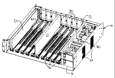
As illustrated in Figures 1 to 5, a first preferred embodiment of the
mounting frame 10 according to the invention contains evenly spaced sets of
opposed
slotted channels or tracks 14, 16, forming compartments for the circuit board
2. An
end compartment 18 contains a chassis 70 supporting the power supplies and
other
high heat-generating components, and the cooling system, as described in
detail
below. One or more dividers 13 may be provided at intermediate positions
within the
mounting frame 10, to isolate compartments (for example the compartment 18
housing chassis 70) and to support the top panel 12 to which tracks 14 are
affixed
(shown only in Figure 3).
CA 02269136 1999-04-16
-9-
The circuit board 30 is illustrated in Figure 12. The circuit board 30
has a rear edge 32 supporting a row of external connectors coupled to the
device
embodied in the circuit (not shown) supported on the circuit board 30. In the
preferred embodiment each external connector comprises the first end 34a of an
adaptor 34, for example one end of an SMB connector, illustrated in Figure 15.
The first end 34a connects to a second end 34b mounted on a connector
plate 36 which is affixed over an opening 20 in the rear of the mounting frame
10.
The connector plate 36 supports at least one row of the external connectors,
preferably
two vertical rows as shown in Figures 12 and 13 to maximize the number of
available
cable connections, facing the interior of the mounting frame 10. On the
exterior face
of the connector plate 36 cable connectors 38, for example BNC type coaxial
cable
connectors, are coupled to the second ends 34b of the adaptor 34. External
analog and
digital signals are thus communicated to and from the circuit board 30 when
the ends
34a, 34b of the adaptor 34 are coupled together. The ends 34a, 34b may be
chamfered
and flared, respectively, to allow for blind coupling of the adaptor 34 with
some
tolerance for misalignment during insertion of the circuit board 30.
In the preferred embodiment the first end 34a is provided with a
compressible snap ring 35 which provides a snap-fit engagement into a groove
(not
shown) formed in the second end 34b. The adaptor 34 is coupled to a BNC
connector
38 by way of example, however it will be appreciated that any other type of
cable
interface can be used to connect the device to external equipment. Examples of
some
other types of connectors are illustrated in Figures 23a to 23d. The
connectors 38, 39
and adaptor 34 should be suitable for the type of signals intended to be
communicated
between the external devices and the circuit board 30.
A row of contacts 40 extends along one long edge of the circuit board
30 abutting the rear edge 32. In the embodiment illustrated in Figure 12 the
contacts
40 are disposed along the bottom edge 31, which is recessed slightly to
accommodate
the height of the connector 50 described below. The contacts 40, preferably
disposed
CA 02269136 1999-04-16
-10-
near the rear edge 32, may comprise one or more power supply connections 40a
for
supplying power to the circuit at the various voltage levels required by the
device,
which may include a ground, and data connections 40b which connect the circuit
to
other devices within the mounting frame 10, for example for high speed data
transmission therebetween.
In alignment with the rear end of the track 16 is a connector 50. The
connector 50 in the preferred embodiment is a releasable connector, or "zero
insertion
force" (ZIF) connector, in which the connector can be disengaged from the
contacts of
the circuit board 30 for insertion or removal. A preferred embodiment is
illustrated in
Figures 6 to 9.
The connector 50 of the invention comprises a housing 52, preferably
plastic, with openings 54 through which the connector pins 56 project when the
connector 50 is closed. The pins 56 are mounted in any suitable fashion to the
bottom
52b of the housing 52, which in turn is secured to the mounting frame 10 as by
clips
58 or by any other suitable means. A top portion 52a of the housing may be
connected to the bottom 52b as by barbed latches 53, or in any other suitable
fashion,
and comprises a slot 52d (shown in Figure 8) into which the bottom edge 31 of
the
circuit board 30 nests when the circuit board 30 is mounted in the connector
50.
The pins 56 each preferably comprise a spring loop 56a for improved
flexibility and resistance to metal fatigue, and a contact arm 56b configured
and
spring biased to provide a stable connection with a contact 40 on the circuit
board 30.
The pins 56 are connected (e.g. soldered) to the data busses and power
conductors (not shown) extending throughout the mounting frame 10 at terminals
56c.
The contact arms 56b are disposed in opposed rows along the insertion path of
the
circuit board 10, as defined by the track 16, impinging into the slot 52d, to
connect
these data busses and power conductors to the appropriate contact 40a or 40b
on the
circuit board 30. In the embodiment illustrated the circuit board 30 has
electrically
independent contacts 40 disposed along both sides of the bottom edge 30a, and
the
CA 02269136 1999-04-16
-11-
connector 50 is thus provided with opposed rows of pins 56 corresponding
thereto.
Preferably the rows of pins 56 are spaced apart so that opposing contact arms
56b
cannot touch one another if the connector 50 is closed with no circuit board
30 in the
connector 50. The circuit board 30 may alternatively have contacts 40 only
along one
side of the bottom edge 31, in which case a single row of pins 56 will be
sufficient. In
either case, preferably the contacts 40 are spaced apart a distance greater
than the
width of a contact arm 56b, so that in case of misalignment of the circuit
board 30 in
the connector 50 the contact arm 56b cannot short circuit adjacent contacts
40.
A cam strip 60, preferably formed from a low-friction plastic and
having opposed laterally extending cams 62 in a sawtooth pattern, is slidably
disposed
through a channel 58 in the housing 52. The cam strip 60 is configured so that
the
cams 62 depress the contact arm 56b of each pin 56 to an open position, shown
in
phantom lines in Figure 8, and recede when shifted longitudinally to a closed
position
so that the contact arms 56b return to a rest position, as shown in solid
lines in Figure
8. To prevent frictional contact between the cam strip 60 and the contact arms
56b, in
the preferred embodiment a gang strip 66, also preferably formed from low-
friction
plastic, is disposed along each row of contact arms 56b to move the entire row
of
contact arms 56a as a unit. The gang strip 66 has cam surfaces 68
complimentary to
the cams 62 on the cam strip 60, to move the rows of contact arms 56b as the
cam
strip 60 is moved longitudinally in the channel 58 between the closed and open
positions, respectively illustrated in Figures 9a and 9b.
It is also possible to move the contact arms 56b differentially, for
example to disengage a power pin before disengaging the ground pin, by
providing
independent cam surfaces 68 actuating one or more specific contact arms 56b
and
having different cam angles, or providing different cam angles to the cams 62
of the
cam strip 60. It will be appreciated that the gang strip 66 will prolong the
life of the
connector 50 by eliminating frictional contact between the cam strip 60 and
the
contact arms 56b, however it is not necessary to the operation of the
connector 50 and
the cam strip 60 can be designed to depress the contact arms 56b by direct
contact.
CA 02269136 1999-04-16
-12-
Thus, when the cam strip 60 is in the open position the cams 62
depress the gang strips 66 in the direction shown by the arrows in Figure 9b,
which in
turn force the contact arms 56b to retract into the housing 52. Preferably
there is no
portion of any pin 56 projecting from the housing 52 in the open position.
When the
cam strip 60 is moved to the closed position, the resilience of the pins 56
causes the
contact arms 56b to move in the direction shown by the arrows in Figure 9a
back to
the rest position where, when a circuit board 30 is connected to the connector
50, the
contact arms 56b couple the back plane circuitry to the circuit board 30
through
contacts 40a, 40b. The cam strip 60 preferably comprises shoulders 60b which
limit
the motion of the cam strip 60 within the housing 52.
In the preferred embodiment the track 16 is used to actuate the cam
strip 60 of the connector 50 in each compartment. In the embodiment of Figure
12 the
track 16 is mounted to the floor of the mounting frame 10 by pins 16a engaging
into
slots (not shown), or is otherwise slidably affixed to the mounting frame 10,
such that
the track can move longitudinally along the compartment with a limited degree
of
motion.
Figure 18 illustrates an alternative embodiment of the mounting frame
in which the compartments are adapted for mounting the circuit boards 30
horizontally, in which case the tracks 14, 16 are provided along dividers 13
between
the compartments. Vents 76 are provided along the side opposite the chassis 70
for
providing an intake airstream to cool the circuit boards 30. The principles of
this
embodiment are otherwise the same as in the embodiment of Figure 12.
The front end of the cam strip 60, which is provided with an
enlargement 60a, is lodged in the rear end of the track 16, as shown in
Figures 10 and
11. Thus, the track 16 forms an actuator for the connector 50. Preferably the
track 16
is in turn actuated by a knob 68 or other obstructing member which is
rotationally
mounted as by a pin 68a and protrudes into the path of the circuit board 30
unless the
knob 68 is turned to the open position, to thus prevent movement of the
circuit board
CA 02269136 1999-04-16
-13-
30 unless the connector 50 is in the open position. Rotation of the knob 68
pulls the
track 16 via eccentric linkage 68b and thus draws the cam strip 60 to the open
position.
In operation, where a circuit board 30 is to be replaced the knob 68 is
rotated to both release the front edge of the circuit board 30 and pull the
track 16,
which draws the cam strip 60 to the open position. The cams 62 coacting with
the
cam surfaces 68 of the gang strips 66 depress the contact arms 56b of the pins
56,
which retract into the housing 52. The circuit board 30 can then be removed by
manually grasping the pull tab 30' at the front of the circuit board 30 and
pulling the
circuit board 30 out of the compartment, which draws the external connectors
34a out
of the mating adaptor portion 34b.
A new circuit board 30 can then be inserted into the tracks 14, 16. As
the circuit board is slid into position the first ends 34a contact and are
depressed into
the second ends 34b, connecting the circuit board 30 to the cable connectors
38 and/or
39. When the circuit board 30 has been fully inserted the knob 68 is turned to
block
movement of the circuit board 30, at the same time pushing the track 18 which
in turn
pushes the cam strip 60 to the closed position shown in Figure 9a. The
resilient action
of the spring loop 56a pushes the contact arms 56b onto the contacts 40a, 40b,
to
connect the device to the back plane circuitry running through the mounting
frame 10.
In embodiments utilizing dual circuit board device, illustrated in
Figures 16 and 17, the front circuit board 30a is connected to the rear
circuit board
30b by an interface adaptor 80 or 82 having connectors at each end that mate
with the
contacts or complimentary connectors along the rear edge of the front circuit
board
30a and along the front edge of the rear circuit board 30b, to integrate the
circuitry of
the device. The interface adaptor may connect to the circuit board 30
transversely, as
in the interface adaptor 80 shown in Figure 16, or may connect to the circuit
board 30
longitudinally as in the interface adaptor 82 shown in Figure 17. Once the
circuit
boards 30a, 30b are connected to form an integral device these embodiments
operates
CA 02269136 1999-04-16
-14-
as in the previously described embodiment. (The external connectors have been
omitted from Figures 16 and 17.)
Figures 21 and 22 illustrate a circuit board group or cluster 90 adapted
for occupying multiple compartments within the mounting frame 10 of Figure 12.
The circuit board cluster 90 comprises circuit boards 92, 94 and 96 which may,
for
example, respectively support circuitry for video, audio and data. The circuit
boards
92, 94 and 96 are integrated into a cluster by a local back plane 98 (cable
connectors
not shown) which provides localized group busses for intercommunication
between
the circuit boards 92, 94 and 96. One or more of the circuit boards 92, 94 and
96 may
also be provided with rows of contacts 40 for connection to the backplane 72
to
integrate the circuit board cluster 90 into the circuitry of the mounting
frame 10
through connectors 50 as hereinbefore described.
Figures 19 and 20 illustrate a preferred cooling system for the
mounting frame of the invention. At least one fan 80 is mounted on a chassis
70
which preferably also supports one or more power supplies and other components
common to the mounting frame 10 and connected to the circuit boards 30 via the
back
plane 72. The chassis 70 is preferably mounted into an end compartment 18,
providing a direct route to the exterior of the mounting frame 10 through
vents 74 to
avoid drawing warm air over the circuit boards 30.
A heat sink tunnel 84 in the form of a cylindrical or inverted "U"-
shaped heat sink is disposed in alignment with the impeller 82, and in the
preferred
embodiment the highest heat generating components are mounted to the heat sink
tunnel 84. The interior opening through the heat sink tunnel 84 preferably
approximates the diameter of the impeller 82, and thus there is negligible
resistance to
air driven out of the mounting frame 10 by the fan 80. At the same time, the
output
airstream efficiently draws heat from the heat sink tunnel 84, to cool the
most
thermally problematic of the mounting frame components.
CA 02269136 1999-04-16
- 15-
The intake airstream draws air from the remainder of the mounting
frame interior, through vents provided in the bottom of the mounting frame 10
as
shown to supply a source of fresh air to the interior of the mounting frame 10
(or in
the case of the horizontally mounted circuit boards in the mounting frame 10
of Figure
18, side-mounted vents 76 provide the fresh air supply). In the preferred
embodiment
all high heat-generating components on the circuit boards 30 are located so as
to be in
the strongest air flow path, in direct alignment with the impeller 82, to
maximize
cooling efficiency. In the preferred embodiment a secondary fan 86 may also
provided, depending upon the number of heat-generating components in any
particular case, expelling air into a second heat sink tunnel 88.
A preferred embodiment of the invention having been thus described
by way of example only, it will be apparent to those skilled in the art that
certain
modifications and adaptations may be made without departing from the scope of
the
invention, as set out in the appended claims. Without limiting the foregoing,
it will be
appreciated that the invention has been described in the context of electronic
audio/video equipment, however the principles and structures used therein are
equally
applicable to other types of electronic equipment and the invention is not
intended to
be limited to the particular embodiments described and shown.