Note: Descriptions are shown in the official language in which they were submitted.
CA 02269566 1999-04-20
r
PHOTORECEPTOR FOR
ELECTROPHOTOGRAPHY
AND METHOD OF MANUFACTURING THE SAME
BACKROUND OF THE INVENTION
(a) Field of the Invention
The present invention relates to a
photoreceptor for electrophotography having an over
to coating layer, and more in particular to the
photoreceptor for electrophotography employed in a
copying machine and a printer using an
electrophotographic recording method.
(b) .Description of the Related Art
i5 Recently, organic photoconductive material has
been widely employed as a photoreceptor for
electrophotography because of its advantages such as
width of material selection and high productivity.
The photoreceptor for electrophotography employing
2o the organic ph.otoconductive material is utilized as a
function-separating photosensitive material
consisting of a charge generation layer and a charge
transport layer layered with each other. '
The photoreceptor for electrophotography is
25 ~ naturally required to have a specified sensitivity,
' CA 02269566 1999-04-20
k 2
electrical characteristics and optical characteristics
depending on an electrophotographic process in
which the above photoreceptor for
electrophotography is employed. Since an electrical
or mechanical force such as that produced in corona
char. grog, toner development, transfer to paper and a
cleaning treatment is directly applied on a surface
layer of the photoreceptor for electrophotography
which can be repeatedly employed, the surface layer
io is required to have high durabilities against the
above force. Due to deterioration produced by ozone
generating during the corona charging, the specific
durabilities are required in connection with
electrical characteristics against sensitivity decrease,
i~ potential decrease and residual potential increase or
those in connection with mechanical characteristics
against abrasion and scratches of the sensitive
material generated by its sliding.
Conventionally, in order to elevate the
2o mechanical durabilities, the employment of
thermosetting or photo-setting resin as an over
coating layer, of the sensitive material is disclosed
(for example, in Patent Publication No. JP-A-1996-
160640, this disclosure will be hereinafter referred to
25 as "prior Art 1"). In accordance with Prior Art 1, a
CA 02269566 1999-04-20
3
photoreceptor for electrophotography having
excellent hardwearing properties and environmental
resistances can be provided by employing a
protective layer having electroconductive metal oxide
s particles dispersed in resin obtained by
polymerization between a photo-setting acryl
monomer and an oligomer, and a photo-
polymerization initiator.
Various coating materials are also known which
io are applied to that other than the sensitive materials.
For example, a curable composition having reactive
silica and a polymerizable unsaturated group
employed as a hard coating material such as a
plastics optical component, a touch panel and glass is
i5 disclosed in Patent Publication No. JP-A-11997-
1007L11 (Title of Invention: "Reactive Silica, its
Preparation and Usage", this disclosure will be
hereinafter referred to as "Prior Art 2").
A coating film having a resistance to scuffing,
~o wealtherability, adherence and curability and
satisfying properties from transparence to
translucence and from high glossiness to dullness
can be formed on various substrates in accordance
with Prior Art 2. These are useful especially for a
protective coating having a resistance to scuffing and
CA 02269566 1999-04-20
w 4
weatherability present on the surface of organic
resin mold, and also useful for a coating material
applicable to a plastic substrate of which a heat
resistant property is poor.
s However, the coating material employing the
thermosetting over coating layer requires a thermal
treatment at a high temperature for a long period of
time:, and this material cannot be used depending on
a kind of an organic photoconductive material a.nd a
io substrate material. Moreover, a further period of
time of the thermal treatment is required for
sufficiently curing the coating material in order to
produce a hardness and a resistance to printing
sufficient for the over coating layer and to stabilize
is the electrophoto characteristics resulting in the
elevation of the manufacturing cost.
When the photo-setting over coating Iayer of
Prior Art 1 is employed, a photo-isomerization
reaction and a photo-decomposition reaction may
20 occur in the organic photoconductive material by
mea~as of an ultraviolet ray which is necessary for the
curing to lower the electrophoto characteristics.
In case of a contact development system in
which toner is rubbed and adhered to the sensitive
2s material at a development part to perform the
CA 02269566 1999-04-20
development, the resistance to printing and the
resi stance to scuffing are insufficient if only the
curable resin is employed in the over coating layer.
In Prior Art 1, the metal particles are dispersed to
5 elevate the electrophoto characteristics, but the
metal particles are likely to be peeled off by repeated
developments, and the peeled-off part
disadvantageously produces an image defect.
When, on the other hand, the coating material
io of Prior Art 2 which is highly resistant is employed
as the over coating layer of the photoreceptor for
electrophotography, the electrophoto characteristics
are largely deteriorated not to put the material in
practice.
i5 In order to prepare the over coating 1 ayer
having the resistance to printing, the hardwearing
property and the resistance to scuffing in the
practical use which is employed in the photoreceptor
for electrophotography of the contact development
~o system, the over coating layer having a thickness
thicker than the coating film of the conventional
plastics optical component is requested. However, a
thick film prepared by employing a conventional
thermosetting and photosetting paint is difficult to
25 be obtained because the paint is contracted at the
CA 02269566 1999-04-20
time of curing. The realization of the film thickness
satisfying not only the electrical characteristics of
the sensitive material or the electrophoto
chap°acteristics but also the high resistance to
printing and the high resistance to scuffing is
extremely difficult.
SUMMARY OF THE INVENTION
It is therefore an object of the present invention
io to provide a photoreceptor for electrophotography
having not only excellent electrophoto characteristics
but also a high resistance to printing and a high
resistance to scuffing, and a method for
manufacturing the same.
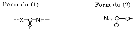
is The present invention provides a photoreceptor
for electrophotography comprising: a substrate, and
an over coating layer layered thereon and prepared
by applying a composition containing silica particles,
an organic compound chemically bonded thereto and
2o a photo polymerization initiator and by curing the
composition; the organic compound having at least
one group selected from a group consisting of a
polymerizable unsaturated group, a group
designated by Formula (1) and a group designated by
2s Formula (2), and the silica particles, and the organic
CA 02269566 1999-04-20
'.. ~ 7
compound being bonded with each other through a
silyloxy group.
Formula (1)
~~~~M~
Formula (2)
.-~ ~..,~-O.-
to
(In these Formulae, -X- is selected from -NH-, -O-
and -S-, -Y- is an oxygen atom or a sulfur atom, and
when -X- is -O-, Y is the sulfur atom)
In accordance with the present invention, the
photoreceptor for electrophotography is obtained
which is excellent not only in durabilities against
ozone and photo-fatigue and a resistance to printing
by means of paper or a cleaning blade but also in
elect~cophoto characteristics such as sensitivity and a
2o residual potential.
BRIEF DESCRIPTION OF DRAWINGS
Fig.l is a sectional view showing a layered
photoreceptor for electrophotography which is an
. Embodiment of the present invention.
CA 02269566 2002-03-06
76826-7
8
Fig. 2 is a flow chart: showing one example of a
method for manufacturing an over coating layer of the
photoreceptor for electrophotography of the present
invention.
Fig. 3 is a graph showing results of an abrasion
test conducted in Exanuples.
PREFERRED EMBODIMENTS OF THE INVENTION
Since, according to the present invention, silica
particles excellent in a resistance to printing and an
organic compound employed as a curing agent are bonded with
each other in an over coating layer coating material, an
over coating layer excellent in durability and in resistance
to printing can be obtained. Since the over coating layer
coating material containing a photo-polymerization initiator
is employed and the coating material can be cured by
employing an ultraviolet ray having a specified wavelength,
a time length for the manufacture can be remarkably
shortened compared with that for the manufacture of an over
coating layer employing a thermosetting coating material,
Furthc=_r, thermal deterioration of performances of an organic
photoconductive materi<~1. and. of a substrate at a time of
curing which is a problem of the thermal curing can be
prevented. Since the thermal ser_t:ing and photo-setting
materials excellent in the resistance to printing and th.e
resistance to scuffing are largely contracted, a thick film
having a thickness of lam or more .required for the over
coating layer of the organic sensiwive material employed in
a conventional contact development is difficult to be
prepared. The over coating layer_ formed as a uniform and
thick film of lam or mc:>re excellent in the resistance to
printing and the resistance to s~~uffing can be prepared
because the contraction at the time of curing can be made
CA 02269566 2002-03-06
76826-7
9
small. by making a bonding among the silica part=icles and the
organic compound whicru is a main curing component.
The photoreceptor according to the invention, when
the over coating layE=_r:~ O.O:L to 10°. by weight of a charge
Gi transfer material., e:~crlibits similar effects to those of the
photoreceptor accordirug to the invention without. the charge
transfer material. By this incorporation of the charge
transport material, the electrophoto-characteristics lowered
by the over coating layer having no added charge transport
material can be improved. For example, the sensitivity is
elevated, and the residual potential is reduced. As a
result, the photoreceptor for el.ectrophotography can be
realized having the e~x.cellent el.ectrophoto-characteristics
and durabilities.
Conventionalllr, metal particles are dispersed in
order to improve the electrophoto-characteristics of the
photoreceptor for electrophc>tography having the over coating
layer. Because of this dispersion, the metal particles are
likely to be peeled off by repeated developments, and the
peeled-off part disadvantageously produces an image defect.
However, when the charge transport material is
incorporated in the over coating layer, strength unevenness
in the over coating layer is removed by adding the charge
transport material having good compatibility with the resin
in the over coating layer. As a result, the partial
peeling-off of the over coating layer is prevented so as to
effectively depress the generation of the image default.
The photoreceptor of the invention, when the over
coating layer has a thickness of 0.5 to l0um, exhibits
similar effects to those of photoreceptor of the invention
described above. Not <:>nly the elevation of the :resistance
to printing and of. the durability but also the suitable
CA 02269566 2002-03-06
76826-7
electrophoto-characteristics in the practical range can be
realized by layering the over coating layer on t=he organic
sensitive material.
When the composition mainly containing the silica
'.i particles, the organic compound chemically bonded thereto
and the photo-polymerization initiator is diluted by and
dispersed in a solvent of whi~~h a main component: is water or
an alcohol having a boiling point of 120°C or less in a
specified concentration range to prepare the photosetting
10 coating material and the coating material is applied and
cured to form the over coating layer, the over coating layer
can be prepared depressing t:he influence of the solvent to
the charge generation layer and to the charge transport
layer that are primary coats for the preparation. In other
words, the over coating layer can be prepared without
dissolution and crystallization of the charge transport
material and crystal transfer of the charge generation layer
by employing the solvent of which the main component is the
alcohol or the water. By making the boiling point of the
solvent for the dilution and the dispersion to be 120°C or
less, the lowering of' the characteristics due to the
residual solvent can be prevented, and the drying treatment
can be conducted in an industrially safe and practical
temperature range which does not effect a thermal influence
to the sensitive material layer to elevate the productivity.
Since the alcohol or the water is employed, the
environmental safety and the relatively easy treatment can
be secured and the environmental problems recently
recognized are suitably avoidable.
A particularly preferred example of the alcohol
having a boiling point of 120°C or less is a mixture of
methanol and isopropyl alcohol. Isopropyl alcohol is
excellent in wettability and is suitable for applying a thin
CA 02269566 2002-03-06
76826-7
11
film employed fox- the over coating layer to a large area. A
mixture of isopropyl al.coho:l with methanol is excellent in
dispersing the composvtion mainly containing the silica
particles, the organic compound chemically bonded thereto
Es and the photo-polymerization initiator. Thus, t:he coating
material can be stably preserved to reduce a drlring speed in
the preparation of the over_ coating layer cornpax,ed with the
case only isopropyl alcohol is employed. Since isopropyl
alcohol forms an azeotropic mixture with water t:o remove
water at a low temperature, moisture affecting the
electrophoto-characteristic: .is not left after the
preparation of the over coating layer for stabilizing the
manufactured sensitive material as well as for preventing
the lowering of the above characteristics. For this reason,
the photoreceptor for electrophotography having excellent
electrophoto-characteristics and excellent durabilities can
be prepared without dissolution and crystallization of the
charge transport 'material and crystal transfer material.
Another aspect of the invention provides a method
for manufacturing a photoreceptor for electrophotography.
A first major embodiment of this aspect comprises:
dissolving a charge transport material into a
first organic solvent which dissolves the charge transport
material at a concentration of 0.5'o by weight or more and
which is other than an alcohol;
diluting the first organic solvent having the
charge transport material dissolved therein with a second
organic solvent that i:~ an alcohol at a specified rate;
dispersing a photosetting coating material in the
diluted organic solvents to prepare a protective coating
material, and
CA 02269566 2002-03-06
7682E~-7
12
applying the over coating layer coating material
to the substrate to .fc:~z:~m the over coating layer.
The first oraganic solvent dissolves a relatively
large amount of the charge transport material. The solvent
in which the charge tx-ansport material is dissolved is
diluted with the alcoholic solvent, and then the photo-
setting coating material is dispersed therein, t:o prepare
the over coating layer coating material. By uniformly
dissolving the charge transport material which hardly
1C dissolves in the photo-setting coating material followed by
the application and the curing in accordance with the above
procedures, the charge transport material is uniformly
dispersed in the over coating layer without precipitation to
prepare the sensitive material without clouding.
A second major embodiment of the methcd aspect,
comprises:
applying an over coating layer coating material;
and
irradiating the over coating layer coating
material with ultraviolet ray having a wavelength of mainly
310 nrn or less to dry and cure the coating material for
forming an over coating layer.
In this embodiment, for curing the over coating
layer coating material, ultravio:Let ray having a wavelength
of mainly 310 nm or less, especially between 254.7 nm and
184.9 nm, is employed. That is, the ultraviolet ray is
absorbed at the neighborhood of. the surface of the over
coating layer by employing that having a high absorption
coefficient concerning the organic material.
CA 02269566 2002-03-06
76826-7
13
Since a photo-is~~mer.izat~ion reaction or a photo-
decomposition reacticxn occurs :in t:he organic maiserial by the
irradiated ultraviolet:: ray, the deterioration, t:he lowering
of the performances and the photo--memory effect of the
organic sensitive material are generated when the photo-
setting coating material is employed. On the contrary, when
the above-mentioned u7.traviolet: ray :is employed, the
lowering of the performances of tr:.e organic sen~~itive
material due to the ultraviolet ray is prevented by
absorbing the ultraviolet ray at the neighborhood of the
organic sensitive mat:er.ial at t:he time of the curing of the
photo-setting coating material, and consequently t:he
photoreceptor for electrophotography having the excellent
electrophoto-characteristics and the excellent durability
can be prepared.
A third majcr embodiment of the method. aspect
comprises:
dissolving a charge transport material into a
first organic solvent. other than an alcohol which dissolves
the charge transport material at a concentration of 0.5% by
weight or more;
diluting the first organic solvent having the
charge transport material dissolved therein with a second
organic solvent that is an alcohol at a specified rate;
dispersing a photosetting coating material in the
diluted organic solvent to prepare an over coating layer
coatlTlg material,
applying the over ccating layer coating material
to the substrate; and
CA 02269566 2002-03-06
7682E>-7
14
irradiating the over coating layer coating
material with ultraviolet ray having a wavelength of mainly
310 nm or less to dry and cure the coating material for
forming an over coating layer.
By this method, the photoreceptor for
electrophotography having excellent. durability, resistance
to printing and electz-ophoto-characteristics can be
effectively prepared a.t a high yiEld. As a result, the
photoreceptor for elec:trophotography having the highly
durable over coating layer can be obtained in a simple
method and at a low cost.
A fourth major embodiment of the method aspect is
for producing the photoreceptor for electrophotc>graphy
mentioned above containing the charge transport material in
the over coating layer. This embodiment comprises:
dissolving a charge transport material into a
first organic solvent. other than an alcohol which dissolves
the charge transport material at a concentration. of 0.5o by
weight or more;
diluting the first organic solvent having the
charge transport material dissolved therein with a second
organic solvent that is an alcohol at a specified rate;
dispersing a r_omposi.tion containing the silica
particles, the organic compound chemically bonded thereto
and the photo-polymerisation initiator in the diluted
organ_Lc solvent to prepare an over coating layer coating
material; and
applying the over coating layer coating material
to the substrate for forming the over coating layer.
CA 02269566 2002-03-06
76826--7
The over coating layer coating material applied
may be irradiated with ultraviolet ray having a wavelength
of mainly 310 nm or less to dry and cure the coating
material.
5 When the first organic solvent is tetrahydrofuran
(THF, the charge transport material can be dissolved therein
at a high concentration. Since the dilution with the
alcoholic solvent is easily performed, THF is preferably
employed in the over coating layer coating material. When
10 the charge transport material is dissolved in the photo-
setting coating material diluted with methanol and isopropyl
alcohol, the dispersi.o:n and the dilution can be performed
without precipitation of the composition thus th.e over
coating layer coating material can be stably prepared.
15 When the second organic solvent is methanol, the
composition of the photo-setting coating material is not
precipitated and easily mixed with THF, whereby the over
coating layer coating material can be stably prepared.
The polymerizable unsaturated group contained in
the organic compound includes, for' example, an acryloxy
group, a methacryloxy group, a vinyl group, a propenyl
group, a butadienyl group, a styryl group, an ethynyl group,
a cinnamoyl group, a maleate group and an acrylamide group,
and an acryloxy group is especially desirable.
Examples of a group designated by the above
Formula (1) include groups identified by the below
Formul ae ( 3 )
Formulae (3)
N H C ---- N H -~ --- S C --- N H
I
0 0
CA 02269566 2002-03-06
76826--7
16
- N H ~ .__.__ N H -__ , ___~ -- ~ -- N H
S
a n d -__ S _._.._ ~ __._.._.. N H __. _. .
5 S
Examples of an organic compound having a group
designated by the above Formula (1) include those identified
by the=_ following formulae:
CA 02269566 1999-04-20
' ' 17
Formulae (4)
(~~~)~.
~1)m
R~=~1-R3-~-C-~-R~-C~1)n R~=~i-R3W-C-~r-R~-(YL)n
d S
-1)m (~1)m
R~=~i'R3-S-C-~-RS-~~1)n R~=~i-R3-S-C-~-R~-~1)n
(~:ljm
R~-Si--R3- O -C-ltlH-R~-~'1.)n
Ii
S
C~1)~
R~-mSi--R3-~-C-hT~-R~-Ice- ;-X-(~2-X-~-hTH-g4-,-~- i -0~p_R~-C~!)n
Y O O O
In these formulae, X'- is an alkoxyl group, a
carboxylate group, a halogen atom, an amino group,
an o:xime group or a hydrogen atom, and R2 is a
hydrogen atom or a mono-valent organic group
having 1 to 8 carbon atoms such as an alkyl group, an
aryl group and an aralkyl group or a non
hydrolyzable organic group comprised of a carbon
2o atom, an oxygen atom and a hydrogen atom.
The alkoxyl group designated by the above X1
includes, for example, a methoxy group, an ethoxy
group, an isopropoxy group, a butoxy group, a
phen~oxy group and an octyloxy group. The
2~ . carboxylate group includes, for example, an acetoxy
CA 02269566 1999-04-20
groL-~p, and the halogen atom includes, for example,
iodine, chlorine, bromine and fluorine. The amino
group includes, for example, a monoalkylamino
group such as a non-substituted amino group a.nd a
met~h.ylamino group and a dialkylamino group such
as a dimethylamino group and a diethylamino group.
The oxime group includes methylene oxime and
dimethylmethylene oxime. In the above formulae,
"m" is 1, 2 or 3. Among these, the alkoxyl group is
io especially desirable.
The alkyl group designated by the above R2
includes, for example, a methyl group, an ethyl group,
a propyl group, a butyl group and an octyl group, and
the aryl group includes, for example, a phenyl group,
1~ a tol.yl group, a xylyl group and a p-methoxyphenyl
group. The aralkyl group includes, for example, a
benzyl group and a phenylethyl group, and the non-
hydrolyzable organic group comprised of the carbon
atom., the oxygen atom and the hydrogen atom
2o inclL-~des, for example, a 2-methoxyethyl group, a 2-
ethoxyethyl group and a 2-butoxyethyl group.
A hydrolyzable silyl group defined by the
combination of the above X1 and R2 preferably
includes, for example, a trimethoxysilyl group, a
~ triethoxysilyl group, a triisopropoxysilyl group, a
CA 02269566 1999-04-20
y 19
methyldimethoxysilyl group and a
dim~ethyldimethoxysilyl group.
The above R3 is selected from bivalent organic
groups having an aliphatic or aromatic structure
having 1 to 12 carbon atoms, and the structure may
contain a chain, branched or cyclic structure. Such a
structural unit includes, for example, methylene,
ethylene, propylene, methylethylene, butylene,
metlhylpropylene, cyclohexylene, phenylene, 2-
to metlzylphenylne, 3-methylphenylne, octamethylene,
biph.enylene and dodecamethylene. Among these, the
methylene, the propylene, the cyclohexylene and the
phenylene are especially preferable.
The above R4 is a bivalent organic group having
1~ an aliphatic or aromatic structure and its structure
may contain a chain, branched or cyclic structure.
Such a structural unit can be selected from a group
consisting of a bivalent organic group having a chain
skeleton structure which includes, for example,
2o methylene, ethylene, propylene, tetramethylene,
hexa~methylene, 2,2,4-trimethylhexamethylene and
1-(methylcarboxyl)-pentamethylene, a bivalent
organic group having an alicyclic skeleton structure
which includes, for example, isophorone,
25 cyclohexylmethane, methylene bis(4-cyclohexane),
' CA 02269566 1999-04-20
hydrogenated diphenylmethane, hydrogenated
xylene and hydrogenated toluene, and a bivalent
organic group having an aromatic skeleton structure
which includes, for example, benzene, toluene,
5 xylene, paraphenylene, diphenylmethane,
diph.enylpropane and naphthalene.
The above X2 is a bivalent organic group, and
more in particular is a bivalent organic group
derived from a compound having, in the molecule,
to two or more active hydrogen atoms which undergo an
addition reaction to an isocyanate group or a
thioi.socyanate group. Examples of this bivalent
organic group include, for example, that derived by
removing two HX- groups from polyalkylene glycols,
15 polyalkylene thioglycols, polyesters, polyamides,
polycarbonates, polyalkylene diamines, polyalkylene
dicarcoxylic acids, polyalkylene diols and
polyalkylene dimercaptanes.
The above "p" is a number of 0, 1 or more, and
2o preferably 1 to 10. When "p" exceeds 10, viscosity of
hydrolyzable silane modified by a polymerizable
unsaturated group tends to be higher and it becomes
intractable.
The above R5 is an organic group having a
2s valency of (n+1) and is selected from, for example, a
CA 02269566 1999-04-20
' ~ 21
chain, branched or cyclic saturated hydrocarbon
group, an unsaturated hydrocarbon group and an
alic3TClic organic group, and "n" is selected from. 1 to
20, and preferably from 1 to 10, and more preferably
3to5.
The above Y~ is a monovalent organic group
having a polymerizable unsaturated group
undE~rgoing an intermolecular crosslinking reaction
under existence of an active radical species. Such a
to group includes, for example, an acryloxy group, a
methacryloxy group, a vinyl group, a propenyl group,
a butadienyl group, a styryl group, an ethynyl group,
a cinnamoyl group, a male ate group and: an
acrylamide, and among these groups, an acryloxy
1~ group is especially desirable.
A photo-polymerization initiator is preferably
selected from compounds generating an active
radical species by means of ultraviolet ray
irradiation, and 0.1 to 10 weight parts thereof,
2o preferably 1 to 5 weight parts is formulated in 100
weight parts of a solid component of the curable
composition.
Examples of the photo-polymerization
initiator includes 1-hydroxy cyclohexyl phenyl
~ ketone, 2,2-dimethoxy-2-phenyl acetophenone,
CA 02269566 1999-04-20
' 22
xant~hone, fluorenone, benzaldehyde, fluorene,
anthraquinone, triphenylamine, carbazol, 3-methyl
acetophenone, 4-chloro acetophenone, 4,4'-dimethoxy
acet~ophenone, 4,4'-diamino benzophenone, Michler's
ketone, benzoisopropyl ether, benzoin ethyl ether,
benzyl dimethyl ketal, 1-(4-isopropylphenyl)-2-
hydroxy-2-methylpropan-1-one, 2-hydroxy-2-methyl-
1-ph.enylpropane-1-one, thioxanthone, diethyl
thioxanthone, 2-isopropyl thioxanthone, 2-chloro
to thioxanthone, 2-methyl-1-[ 4-(methylthio)phenyl]-2-
morpholinopropan-1-one and 2,4,6,-trimethyl
benzoyl Biphenyl phosphine oxide. However, any
material which generates an active radical by light
can be employed, and the photo-polymerization
i5 initiator is not restricted thereto.
Now, the present invention is more specifically
described with reference to accompanying drawings.
Embodiment 1
Referring to Fig.l, a multi-layered
2o photoreceptor for electrophotography 10 is formed by
an electroconductive substrate 11, a charge
generation layer 12, a charge transport layer 1~ and
an over coating layer 14 layered in this turn. The
electroconductive substrate 11 functions as a support
~ for the other layers in addition to as an electrode of
CA 02269566 1999-04-20
' < 23
the photoreceptor for electrophotography, and the
shape thereof may be any form such as cylindrical,
planar and film-like. The material of the substrate 11
is not especially restricted and may be a metal such
as aluminum, stainless steel and nickel. The
substrate 11 may be a composite formed by an
insulation substrate made by glass or plastics and an
electroconductive film such as an aluminum or gold
vapor deposition film and an electrocondu.ctive
io polymer coat, applied thereon.
The charge generation layer 12 is formed by a
vapor deposition film of an organic photocondu.ctive
substance and a coating film prepared by dispersing
an organic charge generation substance in binder
15 resin in which a charge is generated when a charge
generation material receives irradiated light having
a specified wavelength. The charge generation
substance preferably has electrical characteristics
such as a high charge generation efficiency for a
2o wavelength of light employable as a light source and
a high charge injection efficiency for the charge
generation substance employed as the charge
transport layer. The charge generation substance
includes a phthalocyanine compound such as metal-
2~ free phthalocyanine, copper phthalocyanine and
CA 02269566 1999-04-20
' ' 24
titanium oxide phthalocyanine, and a pigment such
as various azo pigments and quinone pigments, and
the material thereof is suitably selected depending
on the wavelength of the light source and the charge
transport substance employed. Since the charge
generation layer 12 absorbs the light from the light
source to generate a sufficient amount of charge for
counteracting a charge on the sensitive material
generated by the corona discharge or the like, the
1o film thickness of the charge generation layer 12 is
determined by such a factor as an absorptivity
coefficient of the charge generation substance, an
amount of the charge generation substance dispersed
in the binder resin and a generation efficiency. The
m thickness is generally 3 ,c.L m or less, and preferably
betv~een 0.1 and 1,c~ m.
The charge transport layer 13 is a coat or the
like formed by a material such as an organic charge
transport substance dispersed in the binder resin.
2o The charge transport layer 13 functions as an
insulation layer in dark, and has a role of retaining a
chap°ge produced by the corona discharge on the
surface of the sensitive material. The charge
transport layer 13 has a function of permeating the
25 light induced by the charge generation layer 12
CA 02269566 1999-04-20
' ' 2~
ther~ethrough and transfers a charge generated in the
charge generation layer 12 and injected thereto at
the time of exposure to neutralize and extinguish the
char°ge on the surface of the sensitive material. An
organic compound such as a hydrazone compound, a
triphenylmethane compound, a triphenylamine
compound and a butadiene compound is employed as
the charge transport material.
Polycarbonate resin, polyester resin, polya.mide
to resin, polyurethane resin, silicon resin and epoxy
resin are employed as the binder resin, which are
required to have a mechanical durability, a chemical
stability, an electrical stability, an adhesion property
with other layers and a compatibility with the charge
m transport material employed. The thickness of the
charge transport layer 13 is determined considering
a charge retention rate, a charge transport speed and
the mechanical durability, and is generally 50 ,c~ m or
less and preferably between 10 and 30 ,c~ m.
2o The over coating layer 14 elevates the
durability and the resistance to printing of the
sensitive material. The layer 14 can sufficiently
endure a mechanical friction produced by, for
example, cleaning, and has a function of retaining a
2s chap°ge on the surface generated by the corona
CA 02269566 1999-04-20
~ 26
discharge or the like in dark and a property of
permeating light induced by the charge generation
layer 12.
The charge transport material is added to the
over coating layer 14 for elevating the electrophoto
characteristics by lowering the electrical resistance
of the over coating layer. The charge transport
material added to the over coating layer may be a
similar material to that conventional employed. An
to organic compound such as a hydrazone compound, a
triplzenylmethane compound, a triphenylamine
compound, a bis-triphenylamine styryl compound
and a butadiene compound is employed as the charge
transport material. Among these compounds, the
is triplzenylamine compound and the bis-
tripl':zenylamine styryl compound are suitable which
are hardly decomposed or isomerized by the
irradiation of an ultraviolet ray.
Although the multilayered photoreceptor for
2o elec~trophotography 10 which consists of the
elecitroconductive substrate 11 made of, for example,
aluminum, the charge generation layer 12, the
charge transport layer 13 and the over coating layer
14 applied and layered in this turn has been
2~ described as one Embodiment, the structure of the
CA 02269566 1999-04-20
~ 27
phoi~oreceptor for electrophotography of the present
invention is not restricted thereto. For example,
anoi;her structure in which a positively charged
sensitive material consisting of the charge transport
layer 13, the charge generation layer 12 and the over
coating layer 14 are layered in this turn on the
electroconductive substrate 11 is included in the
present invention. The charge generation material
can be dispersed in the photosetting resin to make
to the charge generation layer whether it is positively
charged or negatively charged. A single layer
sensitive material is also included in the present
invention which is manufactured by applying a.
coating material obtained by mixing silica particles,
i5 an organic compound chemically bonded thereto, a
phoi;o-polymerization initiator, a charge transport
material and a charge generation material on the
alurxiinum substrate and curing the same.
Then, the over coating layer of the present
2o invention will be described in detail in accordance
with manufacturing procedures shown in Fig.2.
In the method of manufacturing the over
coating layer, for a purpose of elevating the
electrophoto characteristics, a proper quantity of the
2~ chap°ge transport material is added to the over
CA 02269566 1999-04-20
" ~ 28
coating layer. In order to determine the proper
quantity of the charge transport material added to
the over coating layer, an over coating layer coating
material preparation step S 1, an applying step S2, a
solvent drying step S3 and an ultraviolet ray curing
step S4 are conducted in this turn. The over coating
layer coating material preparation step S 1 are
formed by a charge transport material pre-dispersion
step S 1A and a charge transport coating material
to dispersion step S1B.
In the charge transport material pre-dispersion
step S 1A, the charge transport material is dissolved
in a first organic solvent which can be diluted in an
organic solvent contained in a photo-setting coat
m stock solution and in which 10 % or more of the
charge transport material added to the over coating
layer can be diluted, to prepare a thick solution of
the charge transport material. Thereafter, in the
charge transport coating material dispersion step
2o S1B, the above thick solution is dispersed and
dilu7ted in a second organic solvent in which the
charge transport material is difficult to be dissolved
and which can be diluted in an organic solvent
contained in the photo-setting coat, and the photo-
~ setting coat stock solution is dispersed and diluted in
CA 02269566 1999-04-20
' ' 29
the second organic solvent to prepare an over coating
layer coating material.
An organic solvent for diluting and dispersing a
composition mainly containing silica particles, an
organic compound chemically bonded thereto and a
photo-polymerization initiator in a photo-setting
coating material stock solution includes, for example,
a solvent such as methanol, ethanol, isopropyl
alcohol, 2,2-dimethyl-1-propanol, n-butyl alcohol, 2-
io peni;anol, 2-methyl-2-butanol, ethylene glycol,
ethylene glycol monopropyl ether, methyl ethyl
keto~ne, methyl isobutyl ketone, toluene, xylene and
dimethyl forma~nide, and a mixture consisting of
these solvents and an organic solvent compatible
m therewith, and that consisting of these solvents and
water.
An organic solvent for diluting and dispersing
the composition preferably includes alcohols having a
boiling of 120 °C or less. These alcohols include
2o methanol, ethanol, isopropyl alcohol, 2,2-dimethyl-1-
propanol, n-butyl alcohol, 2-pentanol and 2-methyl-
2-butanol. By employing the solvent of which a main
component is the alcohol or the water, the over
coating layer can be prepared while depressing the
2s influence of the solvent to the charge generation
CA 02269566 1999-04-20
' ' 30
layer and to the charge transport layer which a.ct as
primary coats. In other words, the over coating layer
can be prepared without dissolution and
crystallization of the charge transport material and
crystal transfer of the charge generation layer by
employing the solvent of which the main component
is the alcohol or the water.
By making the boiling point of the solvent for
the dilution and the dispersion to be 120 ~ or less,
1o the flowering of the characteristics due to the residual
solvent can be prevented, and the drying treatment
can be conducted in an industrially safe and practical
temperature range which does not effect a thermal
influence to the sensitive material layer to elevate
15 the productivity. Since the alcohol or the water is
employed, the environmental safety and the
relatively easy treatment can be secured and the
environmental problems recently recognized are
suitably avoidable.
2o A more concrete and suitable solvent is a. mixed
solvent of isopropyl alcohol and methanol. The
isopropyl alcohol is excellent in wettability and is
suitable for applying a thin film (about 0.5 to 3 ,ct m)
of the over coating layer to a large area. By mixing
the isopropyl alcohol with the methanol excellent in
CA 02269566 1999-04-20
31
the dispersing ability of the composition mainly
containing the silica particles, the organic compound
chemically bonded thereto and the photo-
polymerization initiator, the coating material can be
stab~ly preserved to reduce the drying speed in the
preparation of the over coating layer compared with
the .case only isopropyl alcohol is employed. Since the
isopropyl alcohol makes an azeotropic mixture with
water to remove the water at a lower temperature,
io moisture affecting the electrophoto characteristics is
not left at the preparation of the over coating layer
for stabilizing the manufactured sensitive material
as well as for preventing the lowering of the above
characteristics.
r5 The first organic solvent includes
dichloromethane, tetrahydrofuran and methyl
ethylketone, and the second organic solvent includes
an alcohol such as isopropyl alcohol, methyl alcohol
and ethyl alcohol, and water.
2o The first organic solvent is preferably
tetrahydrofuran, and the second organic solvent is
preferably methanol. The tetrahydrofuran easily
dissolves the charge transport material and is
excellent in the compatibility with an alcohol. Even
25 when the tetrahyrdofuran is diluted with an alcohol
CA 02269566 1999-04-20
' ' 32
after the charge transport material is once dissolved
in the tetrahydrofuran, the stable dilution of the
charge transport material under a condition of stable
solvation can be realized to achieve the high
concentration in the alcohol. The methanol is
contained in the photo-setting coating material stock
solution and does not precipitate the composition of
the photo-setting coating material. Since the
methanol is easily mixed with the tetrahyrdofuran,
to the stable over coating layer coating material can be
prep are d.
The charge transport material is added to the
ove~~ coating layer 14 of the photoreceptor for
electrophotography of this Embodiment in order to
15 elevate the electrophoto characteristics. A proper
amount of the charge transport material must be
added in the coating material that is employed for
forming the over coating layer 14.
In most cases, the over coating layer 14 is
2o industrially prepared by means of a dip-coating
method. In the procedures for manufacturing the
layered sensitive material 10 shown in Fig.l, the
charge transport material is dissolved at the time of
the dip-coating of the over coating layer from the
25 charge transport layer into the organic solvent which
CA 02269566 1999-04-20
' ' 33
has been employed foic applying the coating material
on the over coating layer 14. The over coating layer
coating material is required to have contradictory
properties such that the coating material dissolves a
s proper amount of the charge transport material and
at the time of forming the over coating layeTC the
coating material does not dissolve the charge
transport material from the charge transport layer
13.
to In order to satisfy this request, a thick solution
is prepared at the charge transport material pre-
dispersion step S 1A and then a proper amount of the
thick solution is diluted in an organic solvent in
which the charge transport material is hardly
m dissolved at the charge transport coating material
dispersion step S 1B. The coating material
preparation according to the procedure prevents the
dissolution of the charge transport material from the
charge transport layer at the time of forming the over
~o coating layer and realizes the over coating layer
coating material which enables the compatible
dissolution of a suitable amount of the charge
transport material in the over coating layer 14.
In the applying step S2, the thus prepared
surface protective coating material is applied on the
CA 02269566 1999-04-20
" ' 34
sensitive material which has been formed by layering
the charge generation layer 12 and the charge
transport layer 13 in this turn on the
electroconductive substrate (supporting substrate)
11. An applying method includes a dip coating, a
spray coating, a blade coating and a ring coating.
In the solvent drying step S3, the solvent which
has been included in the over coating layer coating
material is dried by employing a high temperature
io drier and a vacuum drier. A temperature for the
drying is between a room temperature and that at
which the sensitive material having the applied
coating material is not denaturalized, and generally
between 60 and 150 ~ .
i5 In the ultraviolet ray curing step S4, the
ultraviolet ray irradiation is conducted onto the
coating film from which the solvent has been
removed by the drying to cure the over coating layer
coating material. A preferable wavelength of the
2o ultraviolet ray for curing depends on the photo-
polymerization initiator, and a low-pressure mercury
lamp, a high-pressure mercury lamp and a xenon
lamp are employed as a light source.
A wavelength of 310 nm or less is mainly
25 employed in the present invention as that of the
CA 02269566 1999-04-20
35 '
curing ultraviolet ray. The ultraviolet ray is absorbed
as much as possible at the neighborhood of the
surface by employing that having a high absorption
coefficient concerning the organic material. Since a
phoi~o-isomerization reaction or a photo-
decamposition reaction occurs in the organic
material by the irradiated ultraviolet ray, the
deterioration, the lowering of the performances and
the photo-memory effect of the organic sensitive
1o material are generated when the photo-setting
coating material is employed. The lowering of the
performances of the organic sensitive material due to
the ultraviolet ray is prevented by absorbing the
ultraviolet ray at the neighborhood of the organic
r5 sensitive material at the time of the curing of the
phoi;o-setting coating material, and consequently the
phoi~oreceptor for electrophotography 10 having the
excellent electrophoto characteristics and the
excellent durability can be manufactured. An
2o excimer laser and a low pressure mercury lamp
having main radiation wavelengths of 254.7 nm and
184..9 nm are known as the light source of the
ultraviolet ray having the wavelength of 310 nm or
less. The low-pressure mercury Iamp is suitable for
25 the manufacture of the photoreceptor for
' ' 33
has been employed
CA 02269566 1999-04-20
M 36
electrophotography 10 in which the irradiation must
be conducted to a relatively large area.
The above method of manufacturing the over
coating layer 14 provides the photo-setting over
coating layer 14 having the added charge transport
material, the excellent electrophoto characteristics
and the high durabilities. A suitable thickness of the
over' coating layer 14 changes depending on a
development system and required performances and
to it is generally 10 ,u. m or less, and preferably between
0.5 and 5 ;t~ m in the contact development system.
When the thickness of the over coating layer for the
sensitive material requiring a large area is 0.5 ,t~ m or
less., the preparation of a layer having a uniform
1~ thickness which produces no image irregularity is
difficult and the durability and the resistance to
printing to a development roller and paper are
decreased. When, on the other hand, the thickness
exceeds 5 ,u m, the electrophoto characteristics are
2o considerably lowered, or problems such as increase of
a residual potential and decrease of sensitivity may
be concretely generated to make the sensitivity
material inpracticable.
Although Examples of the present invention
will be described, the present invention shall n.ot be
CA 02269566 1999-04-20
' ~ 37
restricted thereto.
Exam lm a 1
A planar aluminum substrate 11 was dipped in
a liquid prepared by dissolving a charge generation
substance (titanium oxide phthalocyanine) and
bonding resin (butylal resin) into a tetrahydrofuran
(THF) solvent to make a coating film having a dry
thickness of about 0.25 ,u m on the substrate.
A charge transport layer coating material was
to prepared by dissolving a charge transport material
having a below structure (bis-triphenyl amine styryl
compound) and bonding resin (polycarbonate,
tradename: 2200, available from Mitsubishi Gas
Chemical Co.) into the THF solvent. The coating
i5 material was applied on the charge generation layer
12 formerly prepared to make a coating film which
was a charge transport layer 13 having a dry
thickness of about 20 ,u m by means of a dipping
metlhod.
25
CA 02269566 2002-03-06
76826-7
38
Formula 5
Bis-triphenlamine styryl compound
H3 eo oc~3
~----v
N o~ o
o ~o , o
o
H3 C CHs
Then, preparation of the over coating layer 14
is will be described in detail.
At first, 1 weight part of tr~' charge transport
material (bis-triphenyl amine styryl compound) the
same as that employed in the charge transport layer
was dissolved into 10 weight parts of the THF solvent
2o under sufficient agitation (charge transport material
pre-dispersion step S 1A). The thick solution of the
charge transport material thus obtained was diluted
and dispersed in 40 weight parts of isopropyl alcohol.
Then, 50 weight parts of Desolite'~ Z 7501 (JSR
2~ Corporation) which was a coating stock solution
*Trade-mark
CA 02269566 1999-04-20
39
(solvent: methyl ethyl ketone) containing a
composition mainly containing silica particles, an
organic compound chemically bonded thereto and a
photo-polymerization initiator was added to the
diluted solution under sufficient agitation to form an
over coating layer coating material (charge transport
coating material dispersion step S1B). In the over
coating layer coating material thus obtained, the
charge transport material was completely dissolved
to and no precipitation was observed.
The over coating layer coating material thus
obtained was dipped and applied on the charge
transport layer 13 of the sensitive material (applying
step S2). The sensitive material was dried at 00 ~C
is for 20 min. (solvent drying step S3) and irradiated
with. an ultraviolet ray for 1 min. employing a low
pressure mercury lamp (ultraviolet ray curing step
S4) to form the over coating layer 14 having a
thicl~ness of about 1 ,cc m. The curing of the over
2o coating layer 14 and the adhesion property with the
charge transport layer 13 were confirmed by means
of a scratch test of the over coating layer 14 to obtain
the planar photoreceptor for electrophotography 10
of the present invention. No cracks were observed on
2s the surfaces of the charge generation layer 12, o~f the
CA 02269566 1999-04-20
' ' 40
charge transport layer 13 and of the over coating
layer 14 of the photoreceptor for electrophotography
thus obtaine d. Clouding and crystallization in the
respective layers were not observed.
ample 2
The sensitive material having the charge
transport layer 13 prepared in accordance with the
conditions similar to those of Example 1 was dipped
1o in the over coating layer coating material which was
the same as that of Example 1 to form the over
coating layer 14. In this instance, the over coating
layer 14 was prepared by controlling the pull-up
speed in the dipping step to obtain a dry thickness of
3 ,u. m. No cracks were observed on the surfaces of the
charge generation layer 12, of the charge transport
layer 13 and of the over coating layer 14 of the
photoreceptor for electrophotography thus obtained.
Clouding and crystallization' in the respective layers
2o were not observed.
The sensitive material having the charge
transport layer 13 prepared in accordance with. the
conditions similar to those of Example 1 was dipped
CA 02269566 1999-04-20
41
in the over coating Layer coating material which was
the same as that of Example 1 to form the over
coating layer 14. In this instance, the over coating
layer 14 was prepared by controlling the pull-up
speed in the dipping step to obtain a dry thickness of
,cc m. No cracks were observed on the surfaces of the
charge generation layer 12, of the charge transport
layer 13 and of the over coating layer 14 of the
phoi~oreceptor for electrophotography thus obtained.
to Clouding and crystallization in the respective layers
were not observed.
Exam lm a 4
The sensitive material having the charge
transport layer 13 prepared in accordance with the
conditions similar to those of Example 1 was dipped
in the over coating layer coating material which was
the same as that of Example 1 to form the over
coating layer 14. In this instance, the over coating
layer 14 was prepared by controlling the pull-up
speed in the dipping step to obtain a dry thickness of
10 ,u m. No cracks were observed on the surfaces of
the charge generation layer 12, of the charge
transport layer 13 and of the over coating layer 14 of
the photoreceptor for electrophotography thus
CA 02269566 1999-04-20
' ~ 42
obtained. Clouding and crystallization in the
respective layers were not observed.
The photoreceptor for electrophotography 10
was obtained under the same conditions as those of
Example 1 except that 0.5 weight part of the charge
transport material (bis-triphenylamine styryl
compound) was employed in place of 1 weight part
to thereof in Example 1 to form the over coating layer
14. :No cracks were observed on the surfaces of the
charge generation layer 12, of the charge transport
layer 13 and of the over coating layer 14 of the
photoreceptor for electrophotography thus obtained.
1~ CloL~ding and crystallization in the respective layers
were not observed.
Example 6
The photoreceptor for electrophotography 10
2o was obtained under the same conditions as those of
Example 1 except that 0.1 weight part of the charge
transport material (bis-triphenylamine styryl
compound) was employed in place of 1 weight part
thereof in Example 1. No cracks were observed on the
2~ surfaces of the charge generation layer 12, of the
CA 02269566 1999-04-20
' ' 43
charge transport layer 13 and of the over coating
layer 14 of the photoreceptor for electrophotography
thus obtained.
~ Example 7
The photoreceptor for electrophotography 10
was .obtained under the same conditions as those of
Example 1 except that 0.1 weight part of the charge
transport material of the below structure
to (triplzenylamine compound) was employed in place of
1 weight part of the bis-triphenylamine styryl
compound in Example 1.
Formula 6
i~ Triphenylamine Compound
H3C
~0~~~
ao
Comparative Exarn lp_P 1
Photoreceptor for electrophotography in which over
2~ . coating layer was prepared by simply mixed coating
CA 02269566 2002-03-06
76826-7
44
material
The photoreceptor for electrophotography 10
was obtained under the same conditions as those of
Example 1 except that an over coating layer coating
s material prepared by mixing 2 weight parts of the
charge transport material (bis-triphenylamine styryl
compound), 10 weight parts of THF, 50 weight parts
of IPA (isopropyl alcohol) and 50 weight parts of
Desolite Z'7501 and dissolving the material in the
io THF and IPA solvents under agitation for a time
period the same as that of Example 1 was employed.
An over coating layer 14 was formed on the charge
transport layer 13 under the same conditions as
those of Example 1 in connection with the dip
~s application, the solvent drying and the ultraviolet
ray curing. In the over coating layer coating material
thus prepared, the charge transport material was not
completely dissolved. The charge transport material
prepared in accordance with this method was
2o precipitated on the surface of the over coating layer
14 of the photoreceptor for electrophotography, and
this photoreceptor for electrophotography was a
defective.
25 .~''LQ~.na_rative Exam. 2
*Trade-mark
CA 02269566 2002-03-06
76826-7
Photoreceptor for electrophotography in which_over
coating layer was prepared by over coating layer
coating material employing only first solvent THF
The over coating layer 14 was obtained under
5 the same conditions as those of Example 1 except
that an over coating layer coating material prepared
by sufficiently dissolving 1 weight part of the charge
transport material (the bis-triphenylaniine styryl
compound) in 60 weight parts of THF under agitation
io followed by the addition of 50 weight parts of
Desolite 27501 (JSR Corporation) under agitation. In
the over coating layer coating material, the charge
transport material was completely dissolved and was
not precipitated. However, the over coating layer 14
is of the photoreceptor for electrophotography prepared
by employing the above over coating layer coating
material was clouded at the time of the solvent
drying and this photoreceptor for electrophotography
was a defective.
~pa_rative Example 3
Photoreceptor for electrophotography in which no
charge transport material is added to over coating
layer
The photoreceptor for electrophotography 10 for
*Trade-mark
CA 02269566 2002-03-06
76826-7
46
corn:parison was obtained under the same conditions
as those of Example 1 except that the charge
transport material (the bis-triphenylamine ' styryl
compound) was not added. No cracks were observed
s on t:he surfaces of the charge generation layer 12, of
the charge transport layer 13 and of the over coating
layer 14 of the photoreceptor for electrophotography
thus obtained.
io The electrophoto characteristics of the planar
photoreceptor for electrophotography 10 of Examples
1 to 7 and (comparative Examples 1 to 3 were
evaluated employing an Electrostatic Power
Analyzer (EPA-8100, Kawaguchi Electric Works,
i5 Ltd.;) which measures behaviors of a surface potential
of a sensitive material after repeated processes of
charging-exposure-static elimination under the
measurement conditions of -5kV of a corona charged
voltage and 5 Lux of a white exposure and under a
2o room temperature and a normal pressure. The
results were summarized in Table 1. As shown
therein, the photoreceptor for electrophotography 10
of Examples 1 to 7 have excellent electrophoto
characteristics.
*Trade-mark
CA 02269566 1999-04-20
47
Table 1
Sensitivit Residual Thickness Addition
y potential of Concentra
Lux. sec Protective -tion
Layer( ,CG
m)
Example 1 0.231 - 10 1 1
Example 2 0.231 - 20 3 5
Example 3 0.244 - 40 5 5
Example 4 0.265 - 84 10 1
Example 5 0.235 - 19 1 0.5
Example 6 0.231 - 68 1 0.1
Example 7 0.231 - 18 1 0.5
Comp.Ex.1 0.444 -150 or 1 1
more
Comp.Ex.2 non- -500 or 1 1
measu- more
rable
Comp.Ex.3 0.299 -250 or 1 0
more
An over coating layer coating material having a
s charge transport material added thereto at a similar
formulation rate to that of Example 1 was applied on
a disc-like aluminum substrate having thereon a
change transport layer 13 of which a thickness was
about 30 ,cc m. Materials and a formulation rate of the
to charge transport layer were similar to those of
Example 1. After the solvent drying at 90 °C for 20
min., an over coating layer 14 was formed by means
of u=ltraviolet ray curing by employing a low pressure
CA 02269566 2002-03-06
76826-7
48
mercury lamp to manufacture a disc-like abrasion
test, substrate. By employing a Taber abrasion tester
(TABER INDUSTRIES, abrading wheel: MS-10, load
weight: 500 g, 1000 rounds), an abrasion amount was
evaluated to be 0.5 ~c m or less which was an excellent
result.
A charge transport layer 13 having a thickness
m of about 30 ,u m and materials and a formulation rate
which were similar to those of Example 1 was formed
on a disc-like aluminum substrate to prepare a disc-
like abrasion test substrate. A similar abrasion test
to that of Example 8 was conducted, and an abrasion
is amount was 8 ~c m or more which was a bad result.
After samples in which formulation rates of the
charge transport materials in the over coating layers
were changed were prepared in accordance with
2o similar procedures to those of Example 8, abrasion
amounts of the samples were evaluated under the
same conditions.
Fig.3 shows the evaluation results of the
abrasion amounts to the charge transport material
25 addition concentration (CTM addition concentration)
*Trade-mark
CA 02269566 1999-04-20
49
in the over coating layer. In the sensitive material
employing the over coating layer, little abrasion was
observed under the measurement conditions of the
abrasion test, and its hardwearing property was
remarkably elevated compared with the conventional
charge transport layer (Comparative Example 4).
Even if the charge transport material addition
concentration . was 10 %, the abrasion amount of the
over coating layer was 2 ,c~ m or less and accordingly
to the sensitive material had the excellent hardwearing
property.
Exam 1p a 9
A planar aluminum substrate 11 was dipped in
a liquid prepared by dissolving a charge generation
substance (titanium oxide phthalocyanine) and
bonding resin (butylal resin) into a tetrahydrofuran
(THF) solvent to make a coating film having a dry
thicl~ness of about 0.25 ,u m on the substrate.
- A charge transport layer coating material was
prepared by dissolving a charge transport mai;erial
having a below structure (bis-triphenyl amine styryl
compound) and bonding resin (polycarbonate,
tradename: 2200, available from Mitsubishi Gas
Chemical Co.) into the THF solvent. The coating
CA 02269566 1999-04-20
' ' 50
material was applied on the charge generation layer
12 formerly prepared to make a coating film which
was a charge transport layer 13 having a dry
thickness of about 20 ,t~ m by means of a dipping
method.
Formula 6
Bis-triphenlamine styryl compound
N3 ~~ ~~
<? C
ns
Then, preparation of the over coating layer 14
will lbe described in detail.
At first, 1 weight part of the charge transport
2o material (bis~-triphenyl amine styryl compound) the
same as that employed in the charge transport layer
was dissolved into 10 weight parts of the THF solvent
under sufficient agitation (charge transport material
pre-dispersion step SlA). The thick solution of the
~5 charge transport material thus obtained was diluted
CA 02269566 2002-03-06
76826-7
51
and dispersed in 40 weight parts of isopropyl alcohol.
Then, 50 weight parts of Desolite KZ 7861 (JSR
Corporation) which was a coating stock solution
prepared by diluting and dispersing a composition
mainly containing silica particles, an organic
compound chemically bonded thereto and a photo-
polymerization initiator into a mixed solvent
consisting of isopropyl alcohol and methyl ethyl
ketone in ratio of 1:1 was added to the diluted
io solution under sufficient agitation to form an over
coating layer coating material (charge transport
coating material dispersion step S1B). In the over
coating layer coating material thus obtained, the
charge transport material completely dissolved and
is no precipitation was observed.
The over coating layer coating material thus
obtained was dipped and applied on the charge
transport layer 13 of the sensitive material (applying
step S2). The sensitive material was dried at 90 °C
2o for ~?0 min. (solvent drying step S3) and irradiated
with. an ultraviolet ray for 1 min. employing a low
pressure mercury lamp (ultraviolet ray curing step
S3) to form the over coating layer 14 having a
thickness of about 1 ,u m. The curing of the over
25 coating layer 14 and the adhesion property with the
* Tracle -mark
CA 02269566 2002-03-06
76826-7
52
char. ge transport layer 14 were confirmed by means
of a scratch test of the over coating layer 14 to obtain
the planar photoreceptor for electrophotography of
the present invention. No cracks were observed on
the surfaces of the charge generation layer 12, of the
charge transport layer 13 and of the over coating
layer 14 of the photoreceptor for electrophotography
thus obtained. Clouding and crystallization in the
respective layers were not observed.
io A sensitive material drum having the
photoreceptor for electrophotography prepared in
this Example was manufactured and mounted on a
printer PR1000 available from NEC Corporation. As
a result of the printing employing the printer,
is excellent images could be obtained. Further, a
running test of repeated printings were conducted to
find out that the over coating layer had a resistance
to printing three times or more better than that of a
sensitive material drum having no over coating layer.
Exam In a 10
Photoreceptor for electrophotography in which no
charge transport material is added to over coating
layer
The photoreceptor for electrophotography 10 for
*Trade-mark
CA 02269566 1999-04-20
' ' 53
comparison was obtained under the same conditions
as those of Example 9 except that the charge
transport material (the bis-triphenylamine styryl
compound) was not added. No cracks were observed
on the surfaces of the charge generation layer 12, of
the .charge transport layer 13 and of the over coating
layer 14 of the photoreceptor for electrophotography
thus obtained.
io The electrophoto characteristics of the planar
photoreceptor for electrophotography 10 of Examples
9 and 10 were evaluated employing the above
Electrostatic Power Analyzer (EPA-8100, Kawaguchi
Electric Works, Ltd.) under the measurement
1~ conditions of -5kV of a corona charged voltage and 5
Lux of a white exposure and under a room
temperature and a normal pressure. The results were
summarized in Table 2. As shown therein, the
phoi~oreceptor for electrophotography 10 of Examples
20 9 anal 10 have eXCellent electrophoto characteristics.
CA 02269566 1999-04-20
' S4
Tab 1e 2
Sensitivit Residual Thickness Addition
of
y Potential Protective concentra
(Lux.sec) (V) Layer( ,CG -tion (/)
m
Example 9 0.230 - 15 1 1
Example 0.250 about -50 1 ~0
An over coating layer coating material having a
charge transport material added thereto at a similar
formulation rate to that of Example 9 was applied on
a disc-like aluminum substrate having thereon a
charge transport layer 13 of which a thickness was
about 30 ,u m to make an over coating layer 14.
1o Materials and a formulation rate of the charge
transport layer were similar to those of Example 1.
After the solvent drying at 90 °C for 20 min., the
over coating layer 14 was formed by means of
ultraviolet ray curing by employing a low pressure
1~ mercury lamp to manufacture a disc-like abrasion
test substrate. By employing the Taber abrasion
tester (TABER INDUSTRIES, abrasion wheel: 1VJ~S-10,
load weight: 500 g, 1000 rounds), an abrasion amount
was evaluated to be 0.5 ,c~ m or Iess which was an
2o excellent result.
CA 02269566 1999-04-20
' ' 55
ompa_rative Example~-r
A charge transport layer ~3 having a thickness
of about 30 ,t~ m and materials and a formulation rate
which were similar to those of Example 9 was formed
on a. disc-like aluminum substrate to prepare a disc-
like abrasion test substrate. A similar abrasion test
to that of Example 3 was conducted, and an abrasion
amount was 8 ,c~ m or more which was a bad result.
io
Since the above embodiments are described
only for examples, the present invention is not
limited to the above embodiments and various
modifications or alternations can be easily made
i5 therefrom by those skilled in the art without
departing from the scope of the present invention.