Note: Descriptions are shown in the official language in which they were submitted.
CA 02270149 1999-04-27
WO 98I19410 PCT/I1S97118911
1
SINGLE CHIP VLSI IMPLEMENTATION OF A DIGITAL RECEIVER EMPLOYING
ORTHOGONAL FREQUENCY DIVISION MULTIPLEXING
This invention relates to receivers of electromagnetic signals employing
multicarrier modulation. More particularly this invention relates to a digits!
receiver which
is implemented on a single VLSI chip for receiving transmissions employing
orthogonal
frequency division multiplexing) and which is suitable for the reception of
digital video
broadcasts.
Coded orthogonal frequency division multiplexing ("COFDM") has been proposed
for digital audio and digital video broadcasting, both of which require
efficient use of
limited bandwidth, and a method of transmission which is reliable in the face
of several
effects. For example the impulse response of a typical channel can be modeled
as the
sum of a plurality of Dirac pulses having different delays. Each pulse is
subject to a
multiplication factor, in which the amplitude generally follows a Rayleigh
law. Such a
pulse train can extend over several microseconds, making unencoded
transmission at
high bit rates unreliable. In addition to random noise, impulse noise, and
fading, other
major difficulties in digital terrestrial transmissions at high data rates
include multipath
propagation, and adjacent channel interference, where the nearby frequencies
have
highly correlated signal variations. COFDM is particularly suitable for these
applications.
In practical COFDM arrangements, relatively small amounts of data are
modulated onto
each of a large number of carriers that are closely spaced in frequency. The
duration
of a data symbol is increased in the same ratio as the number of carriers or
subchannels, so that inter-symbol interference is markedly reduced.
Multiplexing according to COFDM is illustrated in Figs. 1 and 2, wherein the
spectrum of a single COFDM carrier or subchannel is indicated by line 2. A set
of carrier
frequencies is indicated by the superimposed waveforms in Fig. 2, where
orthogonality
conditions are satisfied. In general two real-valued functions are orthogonal
if
~4~p(t) 4~ q(t) dt = K (1 )
a
where K is a constant, and K = 0 if p ~ q; K ~0 if p = q. Practical encoding
and decoding
of signals according to COFDM relies heavily on the fast Fourier transform
("FFT"), as
can be appreciated from the following equations.
The signal of a carrier c is given by
sc(t) ~ Ac(t)eilw~t+d~~(t)1
CA 02270149 1999-04-27
WO 98/19410 PCT/US97/18911
2
where A~ is the data at time t, w~ is the frequency of the carrier, and ~" is
the phase. N
carriers in the COFDM signal is given by
N
ss(t) - (1/N) ~ An~t)e' ~'~nt'~nc1~
n=o
w" = wo + nOw
Sampling over one symbol period, then
~c ~t) ~ ~n
Ac~t~~An
With a sampling frequency of 1/T, the resulting signal is represented by
N
ss(t) _ (11N) ~ ,(~n(t)e~I(~n+nAw)kT+~n]
n = 00
Sampling over the period of one data symbol r = NT, with wo = 0,
N-1
ss(kT) _ (1/N) ~ Ane~~"e1~"~c~)kT
n = 0
which compares with the general form of the inverse discrete Fourier
transform:
N-1
g(kT) _ (1/N) ~ G(n/(kT))e~nn~k~N> (9)
n=o
In the above equations A"e~~" is the input signal in the sampled frequency
domain, and
ss(kT) is the time domain representation. It is known that increasing the size
of the FFT
provides longer symbol durations and improves ruggedness of the system as
regards
echoes which exceed the length of the guard interval. However computational
complexity increases according to NIogZN, and is a practical limitation.
In the presence of intersymboi interference caused by the transmission
channel,
orthogonaiity between the signals is not maintained. One approach to this
problem has
been to deliberately sacrifice some of the emitted energy by preceding each
symbol in
the time domain by an interval which exceeds the memory of the channel, and
any
multipath delay. The "guard interval" so chosen is large enough to absorb any
intersymbol interference, and is established by preceding each symbol by a
replication
of a portion of itself. The replication is typically a cyclic extension of the
terminal portion
CA 02270149 1999-04-27
WO 98/19410 PCT/US97118911
3
of the symbol. Referring to Fig. 3, a data symbol 4 has an active interval 6
which
contains all the data transmitted in the symbol. The terminal portion 8 of the
active
interval 6 is repeated at the beginning of the symbol as the guard interval
10. The
COFDM signal is represented by the solid line 12. It is possible to cyclically
repeat the
initial portion of the active interval 6 at the end of the symbol.
Transmission of COFDM data can be accomplished according to the known
general scheme shown in Fig. 4. A serial data stream 14 is converted to a
series of
parallel streams 16 in a serial-to-parallel converter 18. Each of the parallel
streams 16
is grouped into x bits each to form a complex number, where x determines the
signal
constellation of its associated parallel stream. After outer coding and
interleaving in
block 20 pilot carriers are inserted via a signal mapper 22 for use in
synchronization and
channel estimation in the receiver. The pilot carriers are typically of two
types. Continual
pilot carriers are transmitted in the same location in each symbol, with the
same phase
and amplitude. In the receiver) these are utilized for phase noise
cancellation, automatic
frequency control, and time/sampling synchronization. Scattered pilot carriers
are
distributed throughout the symbol, and their location typically changes from
symbol to
symbol. They are primarily useful in channel estimation. Next the complex
numbers are
modulated at baseband by the inverse fast fourier transform ("IFFT") in block
24. A
guard interval is then inserted at block 26. The discrete symbols are then
converted to
analog, typically low-pass filtered, and then upconverted to radiofrequency in
block 28.
The signal is then transmitted through a channel 30 and received in a receiver
32. As
is well known in the art, the receiver applies an inverse of the transmission
process to
obtain the transmitted information. In particular an FFT is applied to
demodulate the
signal.
26 A modern application of COFDM has been proposed in the European Telecommu-
nications Standard ETS 300 744 (March 1997), which specifies the framing
structure,
channel coding, and modulation for digital terrestrial television. The
specification was
designed to accommodate digital terrestrial television within the existing
spectrum
allocation for analog transmissions, yet provide adequate protection against
high levels
of co-channel interference and adjacent channel interference. A flexible guard
interval
is specified, so that the system can support diverse network configurations,
while
maintaining high spectral efficiency, and sufficient protection against co-
channel
interference and adjacent channel interference from existing PAL/SECAM
services. The
noted European TelecommunicationsStandard defines two modes of operation. A
"2K
mode", suitable for single transmitter operation and for small single
frequency networks
with limited transmitterdistances. An "8K mode" can be used for either single
transmitter
operation or for large single frequency networks. Various levels of quadrature
amplitude
CA 02270149 1999-04-27
WO 98/19410 PCTIUS97/18911
4
modulation ("QAM") are supported, as are different inner code rates, in order
to balance
bit rate against ruggedness. The system is intended to accommodate a transport
layer
according to the Moving Picture Experts Group ("MPEG"), and is directly
compatible with
MPEG-2 coded TV signals (ISO/IEC 13818).
In the noted European Telecommunications Standard data carriers in a COFDM
frame can be either quadrature phase shift keyed ("QPSK"), 16-QAM, 64-QAM, non-
uniform 16-QAM, or non-uniform 64-QAM using Gray mapping.
An important problem in the reception of COFDM transmission is difficulty in
maintaining synchronizationdue to phase noise and jitterwhich arise from
upconversion
prior to transmission, downconversion in the receiver, and the front end
oscillator in the
tuner, which is typically a voltage controlled oscillator. Except for
provision of pilot
carriers to aid in synchronization during demodulation, these issues are not
specifically
addressed in the noted European Telecommunications Standard, but are left for
the
impiementer to solve.
Basically phase disturbances are of two types. First, noisy components which
disturb neighbor carriers in a multicarrier system are called the "foreign
noise
contribution" ("FNC"). Second, a noisy component which disturbs its own
carrier is
referred to as the "own noise contribution".
Referring to Fig. 5, the position of ideal constellation samples are indicated
by "x"
symbols 34. The effect of foreign noise contribution is stochastic, resulting
in Gaussian-
like noise. Samples perturbed in this manner are indicated on Fig. 5 as
circles 36. The
effects of the own noise contribution is a common rotation of all
constellation points,
indicated as a displacement between each "x" symbol 34 and its associated
circle 36.
This is referred to as the "common phase error", which notably changes from
symbol to
symbol, and must therefore be recalculated each symbol period TS. The common
phase
error may also be interpreted as a mean phase deviation during the symbol
period Ts.
In order for the receiver 32 to process the data symbols in a practical
system, a
mathematical operation is performed on the complex signal representing each
data
symbol. Generally this is an FFT. For valid results to be obtained, a
particular form of
timing synchronization is required in order to align the FFT interval with the
received
data symbol.
It is therefore a primary object of the invention to provide a highly
integrated, low
cost apparatus for the reception of digital broadcasts, such as terrestrial
digital video
broadcasts, which is implemented on a single VLSI chip.
It is another object of the invention to provide an improved method and
apparatus
for synchronizing a received data symbol with an FFT window in signals
transmitted
according to COFDM.
CA 02270149 1999-04-27
WO 98/19410 PCT/LJS97/18911
It is yet another object of the invention to improve the stability of digital
multicarrier
receivers in respect of channel estimation.
It is still another object of the invention to improve the automatic frequency
control
circuitry employed in multicarrier digital receivers.
5 It is a further object of the invention to improve the automatic sampling
rate control
circuitry employed in multicarrier digital receivers.
The invention provides a digital receiverfor multicarriersignalsthat are
transmitted
by orthogonal frequency division multiplexing. The multicarrier signal carries
a stream
of data symbols having an active interval, and a guard interval in which the
guard
interval is a replication of a portion of the active interval. In the receiver
an analog to
digital converter is coupled to a front end amplifier. An I/Q demodulator is
provided for
recovering in phase and quadrature components from data sampled by the analog
to
digital converter, and an automatic gain control circuit is coupled to the
analog to digital
converter. In a low pass filter circuit accepting I and Q data from the I/Q
demodulator,
the I and Q data are decimated and provided to a resampling circuit. An
interpolator in
the resampling circuit accepts the decimated I and Q data at a first rate and
outputs
resampled I and Q data at a second rate. An FFT window synchronization circuit
is
coupled to the resampling circuit for locating a boundary of the guard
interval. A real-
time pipefined FFT processor is operationally associated with the FFT window
synchronization circuit. Each stage of the FFT processor has a complex
coefficient
multiplier, and an associated memory with a lookup table defined therein for
multipli-
cands being multiplied in the complex coefficient multiplier. Each
multiplicand in the
lookup table is unique in value. A monitor circuit responsive to the FFT
window
synchronization circuit detects a predetermined indication that a boundary
between an
active symbol and a guard interval has been located.
According to an aspect of the invention the FFT window synchronization circuit
has
a first delay element accepting currently arriving resampied I and Q data, and
outputting
delayed resampled I and Q data. A subtracter produces a signal representative
of the
difference between the currently arriving resampfed I and Q data and the
delayed
resampled I and Q data. In a first circuit the subtracter output signal is
converted to a
signal having a unipolar magnitude, which is preferably the absolute value of
the signal
provided by the subtracter. A second delay element stores the output signal of
the first
circuit, and a third delay element receives the delayed output of the second
delay
element. In a second circuit a statistical relationship is calculated between
data stored
in the second delay element and data stored in the third delay element. The
output of
the FFT window synchronization circuit is representative of the statistical
relationship.
CA 02270149 1999-04-27
WO 98/19410 PCT/US97/18911
6
Preferably the statistical relationship is the F ratio. The FFT processor is
capable of
operation in a 2K mode and in an 8K mode.
The FFT processor has an address generatorfor the memory of each stage, which
accepts a signal representing the order dependency of a currently required
multiplicand,
and generates an address of the memory wherein the currently required
multiplicand is
stored. In a further aspect of the invention each multiplicand is stored in
the lookup table
in order of its respective order dependency for multiplication by the complex
coefficient
multiplier, so that the order dependencies of the multiplicands define an
incrementation
sequence. The address generator has an accumulator for storing a previous
address
that was generated thereby, a circuit for calculating an incrementation value
of the
currently required multiplicand responsive to the incrementation sequence, and
an
adder for adding the incrementation value to the previous address.
In another aspect of the invention there are a plurality of incrementation
sequences. The multiplicands are stored in row order, wherein in a first row a
first
incrementation sequence is 0, in a second row a second incrementation sequence
is 1,
in a third row first and second break points B1, B2 of a third incrementation
sequence
are respectively determined by the relationships
N-1
B1MN = 4NB9~N-~ 4"
"=o
N
B2M - ~ 4"
N
n=0
and in a fourth row a third break point B3 of a third incrementation sequence
is
determined by the relationship
B3M - 2 x 4N + 2
N
wherein MN represents the memory of an Nth stage of the FFT processor.
The receiver provides channel estimation and correction circuitry. Pilot
location
circuitry receives a transformed digital signal representing a frame from the
FFT
processor, and identifies the position of pilot carriers therein. The pilot
carriers are
spaced apart in a carrier spectrum of the transformed digital signal at
intervals K and
have predetermined magnitudes. The pilot location circuitry has a first
circuit for
computing an order of carriers in the transformed digital signal, positions of
said carriers
being calculated modulo K. There are K accumulators coupled to the second
circuit for
accumulating magnitudes of the carriers in the transformed digital signal, the
accumulated magnitudes defining a set. A correlation circuit is provided for
correlating
CA 02270149 1999-04-27
WO 98I19410 PCT/US97118911
7
K sets of accumulated magnitude values with the predetermined magnitudes. In
the
correlation a first member having a position calculated modulo K in of each of
the K sets
is uniquely offset from a start position of the frame.
According to another aspect of the invention the pilot location circuitry also
has a
bit reversal circuit for reversing the bit order of the transformed digital
signal.
According to yet another aspect of the invention amplitudes are used to
represent
the magnitudes of the carriers. Preferably the magnitudes of the carriers and
the
predetermined magnitudes are absolute values.
in a further aspect of the invention the correlation circuitry also has a peak
tracking
circuit for determining the spacing between a first peak and a second peak of
the K sets
of accumulated magnitudes, wherein the first peak is the maximum magnitude,
and the
second peak is the second highest magnitude.
The channel estimation and correction circuitry also has an interpolating
filter for
estimating the channel response between the pilot carriers, and a
multiplication circuit
for multiplying data carriers output by the FFT processor with a correction
coefficient
produced by the interpolating filter.
The channel estimation and correction circuitry also has a phase extraction
circuit
accepting a data stream of phase-uncorrected i and Q data from the FFT
processor)
and producing a signal representative of the phase angle of the uncorrected
data. The
phase extraction circuit includes an accumulator for the phase angles of
succeeding
phase-uncorrected I and Q data.
According to an aspect of the invention the channel estimation and correction
circuitry includes an automatic frequency control circuit coupled to the phase
extraction
circuit, in which a memory stores the accumulated common phase error of a
first symbol
carried in the phase-uncorrected I and Q data. An accumulator is coupled to
the
memory and accumulates differences between the common phase error of a
plurality
of pilot carriers in a second symbol and the common phase error of
corresponding pilot
carriers in the first symbol. The output of the accumulator is filtered, and
coupled to the
I/Q demodulator.
According to another aspect of the invention the coupled output of the
accumula-
tor of the automatic frequency control circuit is enabled in the I/Q
demodulator only
during reception of a guard interval therein.
According to yet another aspect of the invention the channel estimation and
correction circuitry also has an automatic sampling rate control circuit
coupled to the
phase extraction circuit, in which a memory stores the individual accumulated
phase
errors of pilot carriers in a first symbol carried in the phase-uncorrected I
and Q data.
An accumulator is coupled to the memory and accumulates differences between
the
CA 02270149 1999-04-27
WO 98/19410 PCT/US97/18911
8
phase errors of individual pilot carriers in a second symbol and phase errors
of
corresponding pilot carriers in the first symbol to define a plurality of
accumulated
intersymbol carrier phase error differentials. A phase slope is defined by a
difference
between a first accumulated intersymbol carrier phase differential and a
second
accumulated intersymbol carrier phase differential. The output of the
accumulator is
filtered and coupled to the I/Q demodulator.
According to one aspect of the invention the sampling rate control circuit
stores a
plurality of accumulated intersymbol carrier phase error differentials and
computes a line
of best fit therebetween.
According to another aspect of the invention the coupled output signal of the
accumulator of the automatic sampling rate control circuit is enabled in the
resampling
circuit only during reception of a guard interval therein.
According to an aspect of the invention a common memory for storing output of
the
phase extraction circuit is coupled to the automatic frequency control circuit
and to the
automatic sampling rate control circuit.
According to another aspect of the invention the phase extraction circuit also
has
a pipelined circuit for iteratively computing the arctangent of an angle of
rotation
according to the series
X3 X5 X~ X9
tan-'(x) = x--+---+--. . , ~x~<1
3 5 7 9
wherein x is a ratio of the phase-uncorrected I and Q data.
The pipelined circuit includes a constant coeffccient multiplier, and a
multiplexerfor
selecting one of a plurality of constant coefficients of the series. An output
of the
multiplexer is connected to an input of the constant coefficient multiplier.
According to still another aspect of the invention the pipelined circuit has a
multiplier, a first memory for storing the quantity x2, wherein the first
memory is coupled
to a first input of the multiplier, and has a second memory for holding an
output of the
multiplier. A feedback connection is provided between the second memory and a
second input of the multiplier. The pipelined circuit also has a third memory
for storing
the value of the series. Under direction of a control circuit coupled to the
third memory,
the pipeline circuit computes N terms of the series, and also computes N+1
terms of the
series. An averaging circuit is also coupled to the third memory and computes
the
average of N terms and N+1 terms of the series.
Data transmitted in a pilot carrier of the multicarrier signal is BCH encoded
according to a code generator polynomial h(x). A demodulator operative on the
BCH
encoded data is provided, which includes an iterative pipelined BCH decoding
circuit.
CA 02270149 1999-04-27
WO 98/19410 PCT/US97/18911
9
The BCH decoding circuit is circuit coupled to the demodulator. 1t forms a
Galois Field
of the polynomial, and calculates a plurality of syndromes therewith. The BCH
decoding
circuit includes a plurality of storage registers, each storing a respective
one of the
syndromes, and a plurality of feedback shift registers, each accepting data
from a
respective one of the storage registers. The BCH decoding circuit has a
plurality of
Galois field multipliers. Each of the multipliers is connected in a feedback
loop across
a respective one of the feedback shift registers and multiplies the output of
its
associated feedback shift register by an alpha value of the Galois Field. An
output
Galois field multiplier multiplies the outputs of two of the feedback shift
registers.
A logical network forms an error detection circuit connected to the feedback
shift
registers and to the output Galois field multiplier. The output of the error
detection circuit
indicates an error in a current bit of data, and a feedback line is enabled by
the error
detection logic and connected to the storage registers. Using the feedback
line, the data
output by the feedback shift registers are written back into the storage
registers for use
in a second iteration.
According to an aspect of the invention the output Galois field multiplier has
a first
register initially storing a first multiplicand A, a constant coefficient
multiplier connected
to the first register for multiplication by a value a. An output of the
constant coefficient
multiplier is connected to the first register to define a first feedback loop,
whereby in a
kth cycle of clocked operation the first register contains a Galois field
product Aak. A
second register is provided for storing a second multiplicand B. An AND gate
is
connected to the second register and to the output of the constant coefficient
multiplier.
An adder has a first input connected to an output of the AND gate. An
accumulator is
connected to a second input of the adder, and the Galois field product AB is
output by
the adder.
The invention provides a method for the estimation of a frequency response of
a
channel. It is performed by receiving from a channel an analog multicarrier
signal that
has a plurality of data carriers and scattered pilot carriers. The scattered
pilot carriers
are spaced apart at an interval N and are transmitted at a power that differs
from the
transmitted power of the data carriers. The analog muiticarrier signal is
converted to a
digital representationthereof. A Fouriertransform is performed on the digital
representa-
tion of the multicarrier signal to generate a transformed digital signal. The
bit order of
the transformed digital signal is reversed to generate a bit-order reversed
signal.
Magnitudes of the carriers in the bit-order reversed signal are cyclically
accumulated in
N accumulators, amd the accumulated magnitudes are correlated with the power
of the
- scattered pilot carriers-. Responsive to the correlation, a synchronizing
signal is
CA 02270149 1999-04-27
WO 98/19410 PCT/US97/18911
generated that identifies a carrier position of the multicarrier signal,
preferably an active
carrier.
According to another aspect of the invention the step of accumulating
magnitudes
is performed by adding absolute values of a real component of the bit-order
reversed
5 signal to respective absolute values of imaginary components thereof to
generate sums,
and respectively storing the sums in the N accumulators.
According to yet another aspect of the invention the step of correlating the
accumulated magnitudes also is performed by identifying a first accumulator
having the
highest of the N values stored therein, which represents a first carrier
position, and by
10 identifying a second accumulator which has the second highest of the N
values stored
therein, which represents a second carrier position. The interval between the
first carrier
position and the second carrier position is then determined.
To validate the consistency of the carrier position identification, the
position of a
carrier of a first symbol in the bit-order reversed signal is compared with a
position of a
corresponding carrier of a second symbol therein.
Preferably interpolation is performed between pilot carriers to determine
correction
factors for respective intermediate data carriers disposed therebetween, and
respectively adjusting magnitudes of the intermediate data carriers according
to the
correction factors.
According to an aspect of the invention a mean phase difference is determined
between corresponding pilot carriers of successive symbols of the transformed
digital
signal. A first control signal representing the mean phase difference, is
provided to
control the frequency of reception of the multicarrier signal. The first
control signal is
enabled only during reception of a guard interval.
Preferably a line of best fit is determined for the inter-symbol phase
differences of
multiple carriers to define a phase slope.
For a better understanding of these and other objects of the present
invention,
reference is made to the detailed description of the invention, by way of
example, which
is to be read in conjunction with the following drawings, wherein:
Fig. 1 illustrates the spectrum of a COFDM subchannel;
Fig. 2 shows a frequency spectrum for multiple carriers in a COFDM signal;
Fig. 3 is a diagram of a signal according to COFDM and shows a data symbol
format;
Fig. 4 is a block diagram illustrating an FFT based COFDM system;
Fig. 5 illustrates certain perturbations in a COFDM signal constellation;
Fig. 6 is a flow diagram of a method of timing synchronization according to a
preferred embodiment of the invention;
CA 02270149 1999-04-27
WO 98/19410 PCT/US97I18911
11
Fig. 7 is a plot of an F ratio test performed on several data symbols for
coarse
timing synchronization;
Fig. 8 is a plot of an incomplete beta function for different degrees of
freedom;
Fig. 9 is a plot helpful in understanding a test of statistical significance
according
to the invention;
Fig. 10 is an electrical schematic of a synchronization circuit according to
an
alternate embodiment of the invention;
Fig. 11 is an electrical schematic of a synchronization circuit according to
another
alternate embodiment of the invention;
Fig. 12 is a block diagram of a single-chip embodiment of a digital receiver
in
accordance with the invention;
Fig. 13 is a block diagram illustrating the front end of the digital receiver
shown in
Fig. 12 in further detail;
Fig. 14 is a block diagram illustrating the FFT circuitry, channel estimation
and
correction circuitry of the digital receiver shown in Fig. 12;
Fig. 15 is a block diagram illustrating another portion of the digital
receiver shown
in Fig. 12;
Fig. 16 is a more detailed block diagram of the channel estimation and
correction
circuitry shown in Fig. 14;
Fig. 17 is a schematic of the automatic gain control circuitry of the digital
receiver
shown in Fig. 12;
Fig. 18 is a schematic of the I/Q demodulator of the digital receiver shown in
Fig.
12;
Fig. 19 illustrates in greater detail a low pass filter shown in Fig. 13;
Fig. 20 shows the response of the low pass filter shown in Fig. 19;
Fig. 21 shows the resampling circuitry of the digital receiver shown in Fig.
12;
Fig. 22 illustrates a portion of an interpolator in the resampling circuitry
of Fig. 21;
Fig. 23 is a more detailed block diagram of the FFT window circuitry shown in
Fig.
14;
Fig. 24 is a schematic of a butterfly unit in the FFT calculation circuitry
shown in
Fig.14;
Figs. 25 and 26 are schematics of butterfly units in accordance with the prior
art;
Fig. 27 is a schematic of a radix 22 + 2 FFT processor in accordance with the
invention;
Fig. 28 is 32 point flow graph of the FFT processor shown in Fig. 27;
Fig. 29 is a schematic of a configurable 2K/8K radix 22+2 single path, delay
feedback pipefined FFT processor in accordance with the invention;
CA 02270149 1999-04-27
WO 98/19410 PCT/US97/18911
12
Fig. 30 is a detailed schematic of a complex multiplier used in the circuitry
shown
in Fig. 29;
Fig. 31 is a detailed schematic of an alternate embodiment of a complex
multipliers
used in the circuitry shown in Fig. 29;
Fig. 32 is another diagram illustrating the organization of the twiddle
factors for
each of the multipliers in the circuitry shown in Fig. 29;
Fig. 33 illustrates the organization of the twiddle factors for each of the
multipliers
in the circuitry shown in Fig. 29;
Fig. 34 is a schematic of address generator used in the circuitry shown in
Fig. 29;
Fig. 35 is a schematic of a generalization of the address generator shown in
Fig.
34;
Fig. 36 is a flow chart illustrating the process of pilot location conducted
by the
channel estimation and correction circuitry shown in Fig. 16;
Fig. 37 is a flow chart of an embodiment of the pilot localization procedure
according to the invention.
Fig. 38 is a more detailed block diagram of the tps sequence block of the
circuitry
shown in Fig. 14;
Fig. 39 is a schematic of a BCH decoder used in the tps processing circuitry
shown
in Fig. 38;
Fig. 40 is a more detailed schematic of a Galois field multiplier shown in
Fig. 39;
Fig. 41 is a block diagram generically illustrating the automatic sampling
control
and automatic frequency control loops of the digital receiver shown in Fig.
12;
Fig. 42 is a more detailed block diagram of the automatic sampling control and
automatic frequency control loops shown in Fig. 41;
Fig. 43 is a more detailed block diagram of the phase extract block of the
circuitry
shown in Fig. 42;
Fig. 44 is a schematic of the circuitry employed to calculate an arctangent in
the
block diagram shown in Fig. 43;
Fig. 45 is a plot of the square error at different values of a of the Taylor
expansion
to 32 terms;
Fig. 46 is a plot of the square error at different values of a of the Taylor
expansion
to 31 terms;
Fig. 47 is a plot of the square error at different values of a of the average
of the
Taylor expansion to 31 and 32 terms;
Fig. 48 is a plot of the phase differences of pilot carriers with a line of
best fit
shown;
CA 02270149 1999-04-27
WO 98/19410 PCT/US97/18911
13
Fig. 49 is a more detailed block diagram an alternate embodiment of the
automatic
sampling control and automatic frequency control loops shown in Fig. 41;
Fig. 50 illustrates a coded constellation format used in the demapping
circuitry of
Fig. 15;
Fig. 51 illustrates the conversion of I,Q data to binary data value using the
format
shown in Fig. 50;
Fig. 52 is a more detailed block diagram of the symbol deinterieaving
circuitry
shown in Fig. 15;
Fig. 53 is a more detailed block diagram of the bit deinterleaving circuitry
shown
in Fig. 7 5;
Fig. 54 illustrates the conversion from a coded constellation format to a 24
bit soft
IIQ format by the bit deinterleaving circuitry shown in Fig. 53;
Fig. 55 is a more detailed block diagram of the microprocessor interface of
the
receiver shown in Fig. 12;
Fig. 56 is a more detailed block diagram of the system controller of the
receiver
shown in Fig. 12; and
Fig. 57 is a state diagram relating to channel acquisition in the system
controller
of the receiver shown in Fig. 56.
Alignment of The FFT Window
Referring again to Figs. 3 and 4, according to the invention a statistical
method is
applied to COFDM signals to find the end of the guard interval 10. This method
is
explained with reference to the above noted European Telecommunications
Standard,
but is applicable to many forms of frequency division multiplexing having
prefixed or
postfixed guard intervals. It allows the receiver 32 to find the end of the
guard interval
given only the received sampled complex signal ( solid line 12) and the size
of the active
interval 6 . The method relies on the fact that the guard interval 10 is a
copy of the last
part of the data symbol 4. In the receiver 32, due to echoes and noise from
the channel
and errors in the local oscillator, the guard interval 10 and the last part of
the data
symbol 4 will differ. If the errors introduced are random then a statistical
method can be
applied. According to the invention, the received complex signal is sampled at
a rate
which is nearly identical to that used in the transmitter. A difference signal
is found for
a pair of received samples which are separated by a period of time which is as
close as
possible to the active interval 6. This period should be equal to the size of
the fast
faurier transform ("FFT") being applied {i.e. 2048 or 8192 samples). Let
$i - (Si ~- ~Si_fftsize
CA 02270149 1999-04-27
WO 98I19410 PCT/US97/18911
14
where S; is the difference signal; ~ and $~S;Ze are the current and previous
complex
input samples of which the modules is taken. That is, the subscript "i"
indexes a linear
time sequence of input values. Assuming that the input signal is random, then
S; is also
random. Within the guard interval s; and s;_~S~Zewill be similar, although not
identical, due
to the effects of the channel. S; will be therefore a random signal with a
small dispersion.
As used herein the term "dispersion" means generally the spread of values, and
is not
restricted to a particular mathematical definition. In general the active part
of one symbol
is not related to the active part of the next symbol. Outside of the guard
interval S; will
be random with a much larger dispersion. In order to find the end of the guard
interval,
the dispersion of the difference signal S; is monitored to look for a
significant increase
which wilt occur at the boundary of the guard interval 10 and the active
interval 6. The
inventors have also observed that a large decrease in dispersion is seen at
the start of
the guard interval 10.
According to a preferred embodiment of the invention samples of the input
signal
are stored over an interval which includes at least one symbol period TS. The
dispersion
of the difference signal S; is calculated over a block of samples. The block
is moved
back in time over a number of samples, n, and the dispersion is recalculated.
These two
blocks are referred to herein as "comparison blocks". The ratio of a current
dispersion
in a first comparison block to the dispersion in a previous comparison block
is found.
Then, the F ratio significance test is used to find significant differences in
the
dispersions of the two comparison blocks. The F ratio is defined as
_ VAR(i) (15)
F VAR(i -n)
where n is a positive integer, i indexes the input samples, and VAR(i) is the
variance of
a block of values of length N samples. Variance can be defined as
N 1 N 2
VAR(~~=- ~ (S;_f )2 - -~ S~_~ (16)
N i-o N i=o
While the F ratio significance test is used in the preferred embodiment, other
functions
of the two dispersion values which give a signal relating to the change in
dispersion
could be used. There are many such functions. An advantage of the F ratio is
that for
a random input signal it has a known probability distribution, allowing
convenient
statistical analysis for purposes of performance analysis and system design.
Also the
F ratio intrinsically normalizes the signal, making the result independent of
the signal
level.
CA 02270149 1999-04-27
WO 98/19410 PCT/US97/18911
The method is disclosed with reference to Fig. 6, in which a first member of a
sample pair in a current evaluation block is measured at step 38. A delay of
one active
interval 6 ( Fig. 3) is experienced in step 40. This may be accomplished with
a digital
delay such as a FIFO, or equivalently by buffering samples for an active
interval in a
5 memory and accessing appropriate cells of the memory. A second member of the
sample pair is measured in step 42, and the difference between the first and
second
member is determined and stored in step 44. The end of the current block is
tested at
decision step 46. The size of the evaluation block should not exceed the
length of a
guard interval, and may be considerably smaller. In the event the end of the
current
10 block has not yet been reached, another sample is acquired at step 48, and
control
returns to step 38.
If the end of the current block has been reached, the dispersion of the
current
block is measured in step 50, and is treated as one of two comparison blocks
of data.
A test is made at decision step 52 to determine if a group of two comparison
blocks
15 have been evaluated. If this test is negative, then another block of data
is acquired in
step 54, after which control returns to step 38. The other block of data need
not be
contiguous with the block just completed.
In the event the test at decision step 52 is positive, the F ratio is computed
for the
group of two comparison blocks at step 56. The results obtained in step 56 are
submitted to peak detection in step 60. Peak detection optionally includes
statistical
tests of significance, as is explained hereinbelow.
If peaks are detected, then the boundary of a guard interval is established in
step
62 for purposes of synchronization of the FFT window which is necessary for
further
signal reconstruction. If peaks are not detected, the above process is
repeated with a
block of samples taken from another portion of the data stream.
Exam~ie 1:
Referring now to Fig. 7 a complex signal was generated according to the above
noted European Telecommunicationsstandard using a random number generator, and
transmitted across a Ricean channel model together with added white Gaussian
noise
(SNR = 3.7). Data symbols were then analyzed according to the above described
method. The results 6 data symbols are shown in Fig. 7, wherein the F ratio is
plotted
for convenience of presentation on a logarithmic axis as line 64, because the
spikes 66,
68, at the beginning and end of the guard intervals respectively, are very
large.
Although it is quite evident from Figure 7 that the ends of the guard
intervals are
easy to find using any of several well known peak detectors, it is possible to
apply a
statistical test to more accurately answer the question: do the two blocks of
samples
have the same dispersion? This is the null hypothesis, Ho, i.e. the dispersion
is the
CA 02270149 1999-04-27
WO 98/19410 PCTlUS97/18911
16
same and the observed spike in F is due to random fluctuations only. If Ho has
very low
probability it can be rejected, which would correspond to detection of the
start or end of
the guard interval. From the way the COFDM symbol is constructed Ho is
expected to
be true for comparison blocks lying entirely within the guard interval or
within the active
interval, but false when the comparison blocks straddle a boundary at the
start or end
of the guard interval. If comparison blocks of random samples are drawn from
the same
population then the probability of F is given by
Q(F~v,,v2)-IX( 2 , 2 ) Q17)
where I() is the incomplete Beta function,
v2
x - v2 + v, F C18)
and v~ and v., are the number of degrees of freedom with which the first and
second
dispersions are estimated. In this example v1 = v2 = (N-1 ) if n >= N. The
shape of the
function is shown in Fig. 8. From a statistical point of view n should be
sufficiently large
so that the two blocks do not overlap, i.e. n >= N. If the blocks do overlap,
then the
calculation of the second dispersion will use samples used for the calculation
of the first
dispersion. This effectively reduces the number of degrees of freedom and
hence the
significance of the result. It has been determined that setting n=N works
well.
The function Q() in equation (13) actually gives the one-tailed probability.
Ho could
be rejected if F is either very large or very small, and so the two-tailed
test is required.
Actually the two tails are identical, so for a two-tailed test the probability
is double that
given in equation (13). However, this results in values of probability greater
than one for
F<1. The probability, p, is therefore calculated as follows:
p=21x( 2 ~ 2 )
and then, if (p > 1 ), p = 2 - p. This probability reflects the viability of
Ho. Thus if p is
small, Ho can be rejected and it can be stated, with a specified degree of
certainty, that
the comparison blocks come from sample populations with different dispersion.
The
noted European TelecommunicationsStandard specification states that the block
size,
N, should be 32 for a correlation algorithm. N={32,64} have been successfully
tried. The
probability functions obtained are shown in Fig. 9 using these values for N.
In the
preferred embodiment p <= 0.05 has been set for the rejection of Ho.
CA 02270149 1999-04-27
WO 98/19410 PCT/US97/18911
17
A precise implementationwould be to calculate F, then x, then the incomplete
Beta
function, then p and then apply the threshold test. This algorithm would be
very difficult
to realize in hardware since the Beta function is very complicated. In the
preferred
embodiment it is much simpler, and gives the same results, to set the
acceptance
threshold and N parameter, and thus define an upper and lower limit for F. It
is then only
necessary to calculate F and compare it with the limits. In order to simply
find the end
of the guard interval it may be safely assumed that F> 1. Only the upper limit
on F is
needed. To calculate the limits on F accurately, a suitable root-finding
method, such as
Newton-Raphson may be utilized. Typical values are given in Table 1.
Table 1
p threshold v1 = v2 = v1 = v2 =
31 63
F lower F upper F lower F upper
0.2 0.627419 1.593832 0.722591 1.383909
0.1 0.548808 1.822132 0.658620 1.518326
0.05 0.488143 2.048582 0.607525 1.646022
0.01 0.386894 2.584689 0.518205 1.929738
0.005 0.354055 2.824422 0.487936 2.049448
0.001 0.293234 3.410251 0.429794 2.326695
10'i 4.337235
10'5 5.393528
10-6 6.605896
10-~ 8.002969 '
10-8 9.616664
This method has been successfully tested using the specified channel model
with
additive white Gaussian noise (SNR=3.7).
The formula for dispersion given in Equation (12) would require a multiplier
for
implementation in silicon. The calculation of F is a division in which the (N-
1 )
normalisation constants cancel out as long as the two blocks have the same
size.
Accurate multiplication and division can be expensive in silicon. fn the
preferred
embodiment simplifications have been implemented which give less accurate, but
still
viable, values for F. S; can be assumed to have zero mean so it is not
necessary to
calculate the mean from the block of samples. This also increases the number
of
degrees of freedom from (N-1 ) to N. Instead of calculating variance using the
standard
CA 02270149 1999-04-27
WO 98/19410 PCTlUS97/18911
18
sum of squares formula, the dispersion can be estimated by the mean absolute
deviation. The formula for VAR(i) becomes
N-1
VAR(i)= ~ ~ ~S~_~~ (20)
N ~=o
The (11N) factor divides out in the calculation of F if the two blocks have
the same size.
But there still remains the division of the two dispersions and the squaring
required.
These can be tackled using logarithms to the base 2. Substituting from
Equation (16)
into Equation (11 ) gives
N-, 2 _
~S;_i~
F = i=o - Sa (21 )
N_1 S
S~ _~ -j
j=0
Taking logs to the base 2 gives
log F = 2(log sa - log sb) = y (22)
It is then only necessary to calculate y and compare it with the logarithm to
the base 2
of the F upper limit. The comparison can be made by subtracting the log of the
limit from
2(log2sa-iog2sb) and comparing with zero. The factor of 2 can be absorbed into
the
limit.
Calculation of the logs to base two is relatively straightforward in hardware
if the
numbers are stored as fixed point fractions. The fractions can be split into
an exponent
and a fractional mantissa: x = A2B. Taking log base 2 gives logx = IogA + B.
Since A is
fractional it is practical to find its logarithm using a lookup table. The
exponent B can be
found from the position of the MSB (since sa and sb will both be positive
numbers).
The calculation can thus be reduced to require only addition and subtraction
arithmetic operations. The limit should also be recalculated using v1=v2=N if
using this
method. In practice, the significance level may be set empirically for a
particular
application, preferably p = 0.05.
It will be appreciated by those skilled in the art that various measures of
dispersion
may be utilized without departing from the spirit of the invention, for
example the
CA 02270149 1999-04-27
WO 98/19410 PCT/US97/18911
19
standard deviation, skew, various moments, histograms, and other calculations
known
in the art.
In a first alternate embodiment of the invention, the above described method
is
employed using either the real or the imaginary pans of the signal instead of
the
modulus. This embodiment achieves economy in hardware.
In a second alternate embodiment of the invention, the n parameter of equation
(11) has been optimized. At the end of the guard interval, the two blocks
straddle more
of the transition to the active interval, giving a well-defined increase in
the dispersion.
Using any value n>2 has the drawback that several successive points will give
significant increases as the later block travels up to the boundary. This
small problem
is easily overcome by introducing a dead period after detection of the
boundary. That
is, once a spike has been detected a set of samples equal to the size of the
FFT window
is accepted before further attempts are made to locate another spike. The dead
period
has the added benefit of not introducing false spikes. When using larger
values of n the
spikes 66, 68 ( Fig. 7) increase, whilst the Ho noisy F signal remain much the
same.
Exam,~~le 2:
The maximum F-spike height as a function of n has been measured systematically
together with the background variation in F. The results are shown in Table 2.
Table 2
(1) (2} ~(3) (4) _ (5)
n <F> F F (4) / (3)
3 1.0009 0.07 7.5 107
5 1.0012 0.10 10.7 107
10 1.0011 0.14 12.9 92
15 1.0014 0.17 16.7 98
20 1.0014 0.19 19.3 102
1.0012 0.23 20.9 91
0.9975 0.24 22.0 92
30 50 0.9926 0.25 20.4 81.6
Table 2 was developed using the first 5 frames of the signal analyzed in Fig.
7.
The statistics in columns (2) and (3) of Table 2 were made by excluding any
points
where F>=3.0 to exclude spikes from the calculations. The spikes would
otherwise affect
35 the values of mean and standard deviation even though they are from a
different
statistical population.
CA 02270149 1999-04-27
WO 98/19410 PCT/L1S97/18911
The results indicate that the background variation in F, Fs.d. , was affected
by n,
increasing asymptotically to a value of approximately 0.28. It is likely that
this is the
effect of overlapping blocks. For example, for N=64 and n<64, the blocks over
which the
dispersions are calculated will contain some of the same values and therefore
be
5 correlated. To test this theory Fs.d. was evaluated for n>N, and the results
are shown
in Table 3.
Table 3
n F
60 0.258
10 70 0.266 I
80 0.270
90 0.278
100 0.285
128 0.297
15 256 0.366
The dependence becomes linear at n >= N/2. If F is calculated every n samples,
rather than every sample, then this dependence may be reduced. However, this
creates
a risk for small guard intervals of not having the first block wholly within
the guard
20 interval and the second wholly within the active interval.
A third alternate embodiment of the invention is disclosed with reference to
Fig. 10,
which schematically illustrates a timing synchronization circuit 70. The
circuit accepts
a complex input signal 72, and includes a circuit module 74 which develops the
modulus
of its input, which is taken from node 83. The circuit module 74 insures that
the value
being subsequently processed is an unsigned number. The input to the circuit
module
74 is a difference signal which is developed by a subtracter75 which takes as
inputs the
input signal 72 and a delayed version of the input signal 72 which has been
processed
through a delay circuit 79, preferably realized as a FIFO 77 of length L,
where L is the
size of the FFT window. As explained above, it is also possible to operate
this circuit
where the input signal 72 is real, imaginary, or complex, or even the moduius
of a
complex number. In the case where the input signal 72 is real, or imaginary,
the circuit
module 74 can be modified, and can be any known circuit that removes the sign
of the
output of the subtracter 75, or equivalently sets the sign so that the outputs
accumulate
monotonically; i.e. the circuit has a unipolar output. The output of the
circuit module 74
is ultimately clocked into a digital delay, which is preferably implemented as
a FIFO 78.
When the FIFO 78 is full, a signal SIG1 80 is asserted, and the output of the
FIFO 78
CA 02270149 1999-04-27
WO 98/19410 PCT/US97/18911
21
becomes available, as indicated by the AND gate 82. An adder/subtracter
circuit 84 is
also connected to the node 76, and its output is stored in a register 86. A
delayed
version of the output of the adder/subtractercircuit 84 is taken from the
register 86 and
fed back as a second input to the adder/subtractercircuit 84 on line 88. In
the event the
signal SIG1 80 has been asserted, a version of the output of the circuit
module 74,
delayed by a first predetermined interval N, where N is the number of samples
in the
comparison blocks, is subtracted from the signal on node 76.
The signal on line 88 is an index into a lookup table, preferably implemented
as
a read-only-memory ("ROM"), and shown as ROM 90. The address of the ROM 90
contains the logarithm to the base 2 of the magnitude of the signal on line
88, which
then appears at node 92. The node 92 is connected to a subtracter 94, and to a
delay
circuit, shown as FIFO 98, which is used to develop the denominator of the
middle term
of equation (17).
The subtracter 94 produces a signal which is compared against the logy of a
predetermined threshold value FL,M,T in a comparison circuit 106, shown for
simplicity
as an adder 108 connected to a comparator 110. The output signal SYNC 112 is
asserted when the boundary of a guard interval has been located.
Although not implemented in the presently preferred embodiment) It is also
possible to configure the size of the FIFO 77 dynamically) so that the size of
the interval
being evaluated can be adjusted according to operating conditions. This may
conveniently be done by storing the values on the node 92 in a RAM 114 for
computa-
tion of their dispersion.
In a fourth alternate embodiment of the invention, explained with reference to
Fig.
11, components similar to those of the embodiment shown in Fig. 10 have the
same
reference numerals. A timing synchronization circuit 116 is similar to the
timing
synchronization circuit 70, except now the delay circuit 79 is realized as the
FIFO 77,
and another FIFO 100, one of which is selected by a multiplexer 102. Both of
the FIFOs
77, 100 provide the same delay; however the capacities of the two are
different. The
FIFO 100 provides for storage of samples taken in an interval equal to the
size of the
FFT window, and is normally selected in a first mode of operation, for example
during
channel acquisition, when it is necessary to evaluate an entire symbol in
order to locate
a boundary of a guard interval. In the noted European Telecommunications
standard,
up to 8K of data storage is required, with commensurate resource requirements.
During
subsequent operation, the approximate location of the guard interval
boundaries will be
known from the history of the previous symbols. In a second mode of operation,
It is
therefore only necessary to evaluate a much smaller interval in order to
verify the exact
location of the guard interval boundary. The number of samples used in the
computation
CA 02270149 1999-04-27
WO 98/19410 PCT/CTS97/18911
22
of the dispersion can be kept to a small number, preferably 32 or 64, and the
much
smaller FIFO 77 accordingly selected to hold the computed values. The
resources
saved thereby can be utilized for other functions in the demodulator, and
memory
utilized by the larger FIFO 100 may also be reallocated for other purposes.
A control block 81 optionally advances the evaluation interval relative to
symbol
boundaries in the data stream in successive symbols, and can also be used to
delay for
the dead period. Eventually the moving evaluation interval straddles the
boundary of the
current symbol's guard interval, and synchronization is then determined. The
size of the
evaluation interval is chosen to minimize the use of memory, yet to be large
enough to
achieve statistical significance in the evaluation interval. The size of the
evaluation
interval, and the FIFO 77 may be statically or dynamically configured.
Single Chip Implementation of a COFDM Demodulator
Overview
Referring initially to Fig. 12, there is shown a high level block diagram of a
multicarrier digital receiver 126 in accordance with the invention. The
embodiment
described hereinbelow conforms to the ETS 300 744 telecommunications standard
(2K
mode), but can be adapted by those skilled in the art to operate with other
standards
without departing from the spirit of the invention. A radio frequency signal
is received
from a channel such as an antenna 128, into a tuner 130, which is
conventional, and
preferably has first and second intermediate frequency amplifiers. The output
of the
second intermediate frequency amplifier (not shown), is conducted on fine 132
to an
analog to digital converter 134. The digitized output of the analog to digital
converter
134 is provided to block 136 in which I/Q demodulation, FFT, channel
estimation and
correction, inner and outer deinterleaving, and forward error correction are
conducted.
Carrier and timing recovery are performed in block 136 entirely in the digital
domain, and
the only feedback to the tuner 130 is the automatic gain control ("AGC")
signal which
is provided on line 138. A steady 20 MHz clock on line 140 is provided for use
as a
sampling clock for the external analog to digital converter 134. A host
microprocessor
interface 142 can be either parallel or serial. The system has been arranged
to operate
with a minimum of host processor support. In particular channel acquisition
can be
achieved without any host processor intervention.
The functions performed within the block 136 are grouped for convenience of
presentation into a front end (Fig. 13), FFT and channel correction group
(Fig. 14), and
a back end (Fig. 15).
As shown in Fig. 13, I/Q samples at are received by an IQ demodulator 144 from
the analog to digital converter 134 (Fig. 12) on a bus 146 at a rate of 20
megasamples
per second. An AGC circuit 148 also takes its input from the bus 146. A
frequency rate
CA 02270149 1999-04-27
WO 98/19410 PCT/US97/18911
23
control loop is implemented using a numerically controlled oscillator 150)
which receives
frequency error signals on line 152, and frequency error update information on
line 154.
Frequency and sampling rate control are achieved in the frequency domain,
based on
the pilot carrier information. The frequency error signals, which are derived
from the pilot
carriers, and the frequency error update information will both be disclosed in
further
detail shortly. The I and Q data output from the IQ demodulator 144 are both
passed
through identical low pass filters 156, decimated to 10 megasamples per
second, and
provided to a sinc interpolator 158. Sample rate control is achieved using a
numerically
controlled oscillator 160 which receives sample rate control information
derived from the
pilot signals on line 162, and receives sample error update timing information
on line
164.
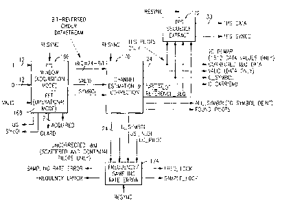
As shown in Fig. 14) acquisition and control of the FFT window are performed
in
block 166, which receives signals from the sinc interpolator 158 (Fig. 13).
The FFT
computations are performed in FFT calculation circuitry 168. Channel
estimation and
correction are performed in channel estimation and correction block 170, and
involves
localization of the pilot carriers, as will be described below in greater
detail. The tps
information obtained during pilot localization is processed in tps sequence
extract block
172. Uncorrected pilot carriers are provided by the circuitry of channel
estimation and
correction block 170 to correction circuitry 174, which develops sampling rate
error and
frequency error signals that are fed back to the numerically controlled
oscillators 150)
160 (Fig. 13).
Referring to Fig. 15, corrected I and Q data output from channel estimation
and
correction block 170 are provided to demapping circuitry 176. The current
constellation
and hierarchical constellation parameters, derived from the tps data, are also
input on
fines 178, 180. The resulting symbols are deinterleaved in symbol
deinterleaver 182,
utilizing a 1512 x 13 memory store. One bit of each cell in the memory store
is used to
flag carriers having insufficient signal strength for reliable channel
correction. Bit
deinterleaver 184 then provides deinterleaved I and Q data to a Viterbi
Decoder 186,
which discards the flagged carriers, so that unreliable carriers do not
influence traceback
metrics. A Forney deinterleaver 188 accepts the output of the Viterbi Decoder
186 and
is coupled to a Reed-Solomon decoder 190. The forward error correction
provided by
the Viterbi and Reed-Solomon decoders is relied upon to recover lost data in
the case
of flagged carriers.
Referring to Fig. 16, in the presently preferred embodiment a mean value is
calculated in block 192 for uncorrected carriers with reference to the
previous symbol.
Data carriers whose interpolated channel response falls below some fraction,
preferably
0.2, of this mean will be marked with a bad carrier flag 194. The bad carrier
flag 194
CA 02270149 1999-04-27
WO 98I19410 PCT/US97/18911
24
is carried through the demapping circuitry 176, symbol deinterleaver 182, and
bit
deinterleaver 184, to the Viterbi Decoder 186 where it is used to discard data
relating
to the unreliable carriers. The parameters used to set the bad carrier flag
194 can be
varied by the microprocessor interface 142.
An output interface 196 produces an output which can be an MPEG-2 transport
stream. The symbol deinterleaver 182, and the bit deinterieaver 184 are
conventional.
The Viterbi decoder 186, Forney deinterleaver 188, Reed-Solomon decoder 7 90,
and
the output interface 196 are conventional. They can be the components
disclosed in
copending Application No. 638,273, entitled "An Error Detection and Correction
System
for a Stream of Encoded Data", filed April 26, 1996, Application No. 480,976,
entitled
"Signal Processing System", filed June 7, 1995, and Application No. 481,107,
entitled
"Signal Processing Apparatus and Method", filed June 7, 1995, all of which are
commonly assigned herewith, and are incorporated herein by reference. The
operation
of the multicarrierdigital receiver 126 (Fig. 12) is controlled by a system
controller 198.
Optionally the hierarchical constellation parameters can be programmed to
speed
up channel acquisition, rather than derived from the tps data.
The input and output signals and the register map of the multicarrier digital
receiver 126 are described in tables 4, and 5 respectively.
Automatic Gain Control
The purpose of the AGC circuit 148 (Fig. 13)is to generate a control signal to
vary
the gain of the COFDM input signal to the device before it is analog-to-
digital converted.
As shown in greater detail in Fig. 17, a Sigma-Delta modulator 200 is used to
provide
a signal which can be used as a gain control to a tuner, once it has been low-
pass
filtered by an external R-C network.
The magnitude of the control voltage signal 202 is given by:
controi_voltage = control_voltage - error (23)
where
error = K ( ~data~ - mean) (24)
where K is a constant (normally K~1 ) which determines the gain in the AGC
control
loop. The mean value can be determined from the statistics of Gaussian noise,
which
is a close approximation to the properties of the COFDM input signal, where
the input
data is scaled to +/-1. The control voltage signal 202 is set back to its
initial value when
the signal resync 204 is set low, indicating a channel change or some other
event
requiring resynchronization.
The input and output signals and the registers for the microprocessorinterface
142
of the AGC circuit 148 are described in tables 6, 7, and 8 respectively.
CA 02270149 1999-04-27
WO 98/19410 PCT/US97/18911
IQ Demodulator
The function of the IO demodulator 144 (Fig. 13) is to recover in-phase and
quadrature components of the received sampled data. It is shown in further
detail in Fig.
18.
5 The numerically controlled oscillator 150 generates in-phase and quadrature
sinusoids at a rate of (32/7) MHz, which are multiplied with data samples in
multipliers
206. The address generator 208 advances the phase linearly. The frequency
error input
210 increments or decrements the phase advance value. The samples are
multiplied
with the sinusoids in the multipliers 206using 10 bit x 10 bit multiply
operations. in one
10 embodiment the 1Q demodulator 144 is operated at 20 MHZ and then retimed to
40MHz
in retiming block 212. In a preferred embodiment the IQ demodulator 144 is
operated
at 40MHz, in which case the retiming block 212 is omitted.
Sinusoids are generated by the address generator 208 on lines 214, 216. The
phase value is employed as an address into a lookup table ROM 218. Only
quarter
15 cycles are stored in the lookup table ROM 218 to save area. Full cycles can
be
generated from the stored quarter cycles by manipulating the data from the ROM
218
and inverting the data in the case of negative cycles. Two values are read
from the
lookup table ROM 218 for every input sample -- a cosine and a sine, which
differ in
phase by 90 degrees.
20 The input and output signals of the IQ demodulator 144 are described in
tables 9
and 10 respectively.
Low Pass Filter
The purpose of the low pass filters 156 (Fig. 13) is to remove aliased
frequencies
after lQ demodulation - frequencies above the 32I7 MHz second IF are
suppressed by
25 40dB. I and Q data are filtered separately. The output data is decimated to
10
megasamples per second ("Msps") because the filter removes any frequencies
above
1/4 of the original 20 Msps sampling rate. The filter is constructed with
approximately
60 taps which are symmetrical about the center, allowing the filter structure
to be
optimized to reduce the number of multipliers 220. Fig. 19 is a block diagram
of one of
the low pass filters 156, the other being identical. Fig. 19 shows a
representative
symmetrical tap 222) and a center tap 224. The required fitter response of the
low pass
filters 156 is shown in Fig. 20.
The input and output signals of the low pass fitters 156 are described in
tables 11
and 12 respectively.
Resampfing
Referring to Fig. 13, the purpose of resampling is to reduce the 10 Msps data
stream output from the low pass filters 156 down to a rate of (64I7) Msps,
which is the
CA 02270149 1999-04-27
WO 98/19410 PCT/US97/18911
26
nominal sample rate of the terrestrial digital video broadcasting ("DVB-T")
modulator at
the transmitter.
Resampling is accomplished in the sinc interpolator 158, and the numerically
controlled oscillator 160. The latter generates a nominal 64I7 MHZ signal. The
resampling circuitry is shown in further detail in Fig. 21. The numerically
controlled
oscillator 160 generates a valid pulse on line 226 and a signal 228
representing the
interpolation distance for each 40MHz clock cycle in which a 64/7MHz sample
should
be produced. The interpolation distance is used to select the appropriate set
of
interpolating f Iter coefficients which are stored in coefficient ROMs 230. It
should be
noted that only the sinc interpolatorfor I data is illustrated in Fig. 21. The
structures for
Q data are identical.
Fig. 22 illustrates the generation of the interpolation distance and the valid
pulse.
Nominally TS = 1/10 Msps, and T = 1 / (64I7) Msps. The sinc interpolation
circuit
disclosed in our noted Application No. 08I638,273 is suitable, with
appropriate
adjustment of the operating frequencies.
The input and output signals of the sinc interpolator 158 and the numerically
controlled oscillator 160 are described in tables 13 and 14 respectively.
FFT Window
As has been explained in detail above, the function of the FFT Window function
is to locate the "active interval" of the COFDM symbol, as distinct from the
"guard
interval". This function is referred to herein for convenience as "FFT
Window". In this
embodiment the active interval contains the time domain representation of the
2048
carriers which will be recovered by the FFT itself.
The FFT window operates in two modes; Acquisition and Tracking. In Acquisition
mode the entire incoming sample stream is searched for the guard
interval/active
interval boundary. This is indicated when the F-ratio reaches a peak, as
discussed
above. Once this boundary has been located, window timing is triggered and the
incoming sample stream is searched again for the next guard interval/active
interval
boundary. When this has been located the length of the guard interval is known
and the
expected position of the next guardlactive boundary can be predicted. The FFT
window
function then switches to tracking mode.
This embodiment is similar to the fourth alternate embodiment discussed above
in respect of the tracking mode. In tracking mode only a small section of the
incoming
sample stream around the point where the guardlactive boundary is expected to
be is
searched. The position of the active interval drifts slightly in response to
IF frequency
and sampling rate offsets in the front-end before the FFT is calculated. This
drift is
CA 02270149 1999-04-27
WO 98/19410 PCT/US97/18911
27
tracked and FFT window timing corrected, the corrections being inserted only
during the
guard interval.
It will be appreciated by those skilled in the art that in a practical single
chip
implementation as is disclosed herein, memory is an expensive resource in
terms of
chip area, and therefore must be minimized. Referring to Fig. 23, during
Acquisition
mode the FFT calculation process is not active so hardware can be shared
between the
FFT Window and the FFT calculation, most notably a 1024x22 RAM 232 used as a
FIFO by the FFT Window, and selected for receipt of FFT data on line 234 by a
multiplexer 236. Once in Tracking mode the FFT calculation process is active
so that
other control loops to recover sampling rate and frequency which depend on FFT
data
(e.g. pilots in the COFDM symbol) can initialize. Therefore tracking mode
requires a
dedicated tracking FIFO 238, which is selected by a multi~lexer 240.
The input and output signals, and signals relating to the microprocessor
interface
142 of the FFT Window circuitry shown in Fig. 23 are described in tables 15,
16, and 17
respectively.
In one embodiment a threshold level, set from statistical considerations, is
applied
to the F-ratio signal (see Fig. 7) to detect the negative and positive spikes
which occur
at the start and end of the guard interval respectively. The distance between
the spikes
is used to estimate the guard interval size. Repeated detection of the
positive spikes is
used to confirm correct synchronization. However with this method under noisy
conditions the F-ratio signal becomes noisy and the spikes are not always
reliably
detectable.
In another embodiment peak detection is used to find the spikes in the F-
ratios.
It has been found that a fixed threshold is reliable only at or exceeding
about a carrier-
to-noise ("C/N") ratio of 12 dB. Peak detection is generally more sensitive
and more
specific, with generally reliable operation generally at 6 - 7 dB. The maxima
should
occur at the end of the guard interval. The difference in time between the two
maxima
is checked against the possible guard interval sizes. With an allowance for
noise, the
difference in time indicates the most likely guard interval size and the
maxima
themselves provide a good indication of the start of the active part of the
symbol.
Preferably this process is iterated for several symbols to confirm detection,
and is
expected to improve performance when the C/N ratio is low.
The data stream is passed to accumulators 242, 244, each holding 64 moduli.
Conversion to logarithms and subtraction of the logarithms is performed in
block 246.
The peaks are detected in peak detector block 248. Averaging of the symbol
peaks is
performed in block 250.
CA 02270149 1999-04-27
WO 98/19410 PCT/US97/18911
28
In noisy conditions, the maxima may be due to noise giving possibly inaccurate
indications of the guard interval length and the start of the active symbol.
The general
strategy to cope with this is to perform a limited number of retries.
Currently, calculation of the F-ratio is done "on the fly" i.e. only once at
each point.
The variance estimates are calculated from 64 values only. Under noisy
conditions, the
variance estimates become very noisy and the spikes can become obscured. In an
optional variation this problem is solved by obtaining more values for the
variance
estimate, by storing the variance estimate during acquisition for each of the
possible
T+GmaX Points in the storage block 256. The variance estimates themselves may
be
formed by accumulating variances for each point, and then filtering in time
over a
number of symbols. A moving average filter or an infinite impulse response
("IiR") filter
is suitable. A moving run of symbols, preferably between 16 and 32, are
integrated in
block 252, which increases the reliability of peak detection under noisy
conditions. The
storage block 256 holding the integrated F-ratio values is searched to find
the maximum
value. This is of length T+GmaX, where GmaX is the maximum guard interval
size, T/4.
Preferably the memory for storage block 256 is dynamically allocated,
depending on
whether acquisition mode or tracking mode is operative. Any unused memory is
released to other processes. Similarly in tracking mode the integrated data
stream is
stored in tracking integration buffer 254.
This method has been tested with up to 4 symbols, without an IIR filter, and
it has
been found that the spikes can be recovered. However this approach does
require
increased memory.
FFT Processor
The discrete Fourier transform ("DFT") has the well known formula
x(k) _ ~ ~ x(n)W "k k = 0,1,...,N-1 (25)
n=0
where N = the number of points in the DFT;
x(k) = the kth output in the frequency domain;
x(n) = the nth input in the time domain
and
W nk = a -j(2nnklL)
L
W is also known as a "twiddle factor".
For N > 1000 the DFT imposes a heavy computational burden and becomes
impractical. instead the continuous Fourier transform is used, given by
CA 02270149 1999-04-27
WO 98/19410 PCT/US97/18911
29
x(t) _ ~ x(t)e -t~'tdt (27)
t
The continuous Fourier transform, when computed according to the well known
FFT
algorithm, breaks the original N-point sequence into two shorter sequences. In
the
present invention the FFT is implemented using the basic butterfly unit 258 as
shown
in Fig. 24. The outputs C and D represent equations of the form C = A + B, and
D = (A
B)W~'. The butterfly unit 258 exploits the fact that the powers of W are
really just
complex additions or subtractions.
A real-time FFT processor, realized as the FFT calculation circuitry 168 (Fig.
14)
is a key component in the implementation of the multicarrier digital receiver
126 (Fig.
12). Known 8K pipeline FFT chips have been implemented with 1.5M transistors,
requiring an area of 100 mm2 in 0.5N technology, based on the architecture of
Bi and
Jones. Even using a memory implementation with 3-transistor digital delay line
techniques, over 1 M transistors are needed. This has been further reduced
with
alternative architecture to 0.6M, as reported in the document A New Approach
>~o
Pipeline FFT Processor. Shousheng He and Mats Torkelson, Teracom Svensk
RundRadio. DTTV-SA 180, TM 1547. This document proposes a hardware-oriented
radix-22 algorithm. having radix-4 multiplicative complexity. However the
requirements
of the FFT computation in the present invention require the implementation of
a radix
22+2 FFT processor.
Referring to Fig. 25 and Fig. 26 the butterfly structures BF21 260 and BF211
262,
known from the noted Torkelson publication, are shown. The butterfly structure
BF211
262 differs from the butterfly structure BF21 260 in that it has logic 264 and
has a
crossover 266 for crossing the real and imaginary inputs to facilitate
multiplication by -j.
Fig. 27 illustrates the retimed architecture of a radix 2' + 2 FFT processor
268 in
accordance with the invention, which is fully pipelined, and comprises a
plurality of
stages, stage-0 270 through stage-6 272. Except for stage-0 27d, the stages
each
comprise one butterfly structure BF21 260 and one butterfly structure BF211
262, and
storage RAMS 274, 276 associated therewith. stage-0 270 only has a single
butterfly
structure BF21 260. This architecture performs a straight-forward 32-point
FFT. stage-6
272 has control logic associated therewith, including demultiplexer 278 and
multiplexer
280, allowing stage-6 272 to be bypassed, thus providing a 2K implementation
of the
FFT. Counters 282 configure the butterfly structures BF21 260 and BF211 262 to
select
one of the two possible diagonal computations, during which data is being
simulta-
neously written to and read from the storage RAMS 274, 276.
CA 02270149 1999-04-27
WO 98/19410 PCT/US97/18911
Fig. 28 illustrates a 32 point flow graph of the FFT processor 268 using radix
22+2
pipeline architecture. Computations are performed using eight 4-point FFTs and
four 8-
point FFTs. These are decomposed in turn into two 4-point FFTs and four 2-
point FFTs.
Fig. 29 illustrates the retimed architecture of a configurable 2K/8K radix
22+2
5 single path, delay feedback pipelined FFT processor 284, in which like
elements in Fig.
27 are given the same reference numerals. The stages have a plurality of
pipeline
registers 286 which are required for proper timing of the butterfly structures
BF21 260
and BF211 262 in the various stages. As can be seen, the addition of each
pipelined
stage multiplies the range of the FFT by a factor of 4. There are 6 complex
multipliers
10 288, 290, 292, 294, 296) 298 which operate in parallel. This processor
computes one
pair of I/Q data points every four fast clock cycles, which is equivalent to
the sample rate
clock. Using 0.35Nm technology the worst case throughput is 140Ns for the 2K
mode of
operation, and 550Ns for the 8K mode, exceeding the requirements of the ETS
300 744
telecommunicationsstandard. Data enters the pipeline from the left side of
Fig. 29, and
15 emerges on the right. The intermediate storage requirements are 2K/8K for I
data and
2K/8K for Q data, and is mode dependent. In practice the radix-4 stage is
implemented
as a cascade of two adapted radix-2 stages that exploit the radix-4 algorithms
to reduce
the number of required complex multipliers.
Fig. 30 is a schematic of one embodiment of the multipliers 288, 290, 292,
294,
20 296) 298 for performing the complex multiplication C = A x B, where A is
data, and B is
a coefficient. Because the FFT processor 284 has 6 complex multipliers, each
requiring
3 hardware multipliers 300, a total of 18 hardware multipliers 300 would be
required. It
is preferable to use the embodiment of Fig. 31 in which some of the hardware
multipliers
300 are replaced by multiplexers 302, 304.
25 Turning again to Fig. 29 there are a plurality of RAMS 306, 308, 310, 312,
314,
316 which are preferably realized as ROMs and contain lookup tables containing
complex coefficients comprising cosines for the multipliers 288, 290, 292,
294, 296, 298
respectively. It has been discovered that by addressing the RAMS 306) 308,
310, 312,
314, 316 according to a particular addressing scheme, the size of these RAMS
can be
30 markedly reduced. The tradeoff between the complexity of the addressing
circuitry and
the reduction in RAM size becomes favorable beginning at stage-3 318.
Referring again
to Fig. 28 there are two columns 320, 322. Column 320 holds values WZ - W'4,
followed
by W' - W7, and then W3 - W2'. These coefficients are stored in the RAM 308,
required
by the particular multiplier 290. Column 322 contains values V11, W4, W'2,
which repeat
3 times. Note furtherthat between the values W8, W4, and W4, W'2 are
connections 324,
326 to the preceding butterfly unit located in column 328. In practice the
connections
324, 326 are implemented as multiplications by W~. In moving from multiplier
to
CA 02270149 1999-04-27
WO 98/19410
PCT/US97/18911
31
multiplier toward the left in Fig. 29, the lookup table space is multiplied by
a power of 4
at each stage. In Fig. 32 table 330, the lookup table for multiplier M3
contains 512
entries. It can be deduced by extrapolation that multiplier M5 must contain
8192 twiddle
factors, and corresponds to the size of the FFT being performed by the FFT
processor
284 (Fig. 29).
Before examining the look-up table space in more detail it is helpful to
consider the
plurality of horizontal lines 332. Moving downward from the top of Fig. 28,
the line
beginning at x(3) extends to W8, which is the first twiddle factor required)
and is at the
third effective step in the flow diagram. Figs. 33 and 32 show the
organization of the
twiddle factors for each of the multipliers, wherein the terminology Mk
represents the
multiplier associated with the kth stage. Thus table 334 relates to multiplier
Mo. The
notation for the W values (twiddle factors) is shown in box 336. The subscript
"B" at the
bottom right represents a time stamp, that is an order dependency in which the
twiddle
factors are required by the pipeline. The superscript "A" represents the
address of the
twiddle factor in its lookup table. The superscript "N" is the index of the
twiddle factor.
Thus in table 334 it may be seen that W~ is required at time 0, W~ at time 1,
and
W~ is again required at time 2. Further inspection of the other tables in
Figs. 33) 32
reveals that half of the entries in each table are redundant. The storage
requirement for
the lookup tables can be decreased by 50% by eliminating redundant entries.
This has
been accomplished by organizing the W values in ascending order by index, so
that the
values can be stored in memory in ascending order, Thus in the case of table
338 the
index values range from 0 to 21, with gaps at 11, 13, 16, 17, 19, and 20.
The procedure for organizing the lookup table and the addressing scheme for
accessing the twiddle factors is explained with reference to table 338, but is
applicable
to the other tables in Fig. 33. (1 ) Each row is assigned a line number as
illustrated. (2)
Each twiddle factor is assigned an order dependency which is noted in the
lower right
of its respective cell in table 338. (3) It is assumed that table 338 in its
reduced form will
contain only unique twiddle factors in ascending order by index within the
memory
address space. Consequently each twiddle factor is assigned a memory address
as
shown in the upper left of its respective cell.
During address generation, for line 3 of table 338 the address is simply held
at 0.
For line 1 the address is incremented by 1 to the end of the line. However
lines 0 and
2 contain non-trivial address sequences. For line 0, looking at table 340,
which contains
64 values, it will be observed that the address sequence changes according to
the
intervals 2,2,2,2, and then later 1,1,2,1,1,2 ... For line 2, the address
first increments by
3, then by 2, and finally by 1. The locations at which the address increments
change are
CA 02270149 1999-04-27
WO 98/19410 PCT/LTS97/1$911
32
referred to herein as the "break-points". These values of the break points
range between
0, corresponding to the first point in line 2, to the last position in the
line.
By inspection it can be seen that the occurrence of the first break point
changes
from table to table following the recurrence relationship
B1 MN = 4B1 MN_~ (28)
with the initial condition
B 1 M~ = 1 (29)
where MN is the multiplier of the Nth stage of the FFT processor 284.
Expanding the recurrence relationship gives:
B1MN = (((4B1M~-1)x4-1)x4-1) ... (30)
B1 M = 4N81 M _4N-3 -4N-2... -40 ( )
31
N 0
N-1
B1 MN = 4NB1 MN -~ 4" (32)
n =0
Similarly the second break point B2 for line 2 is determined from the
recurrence relation
B2M = 482M + 1 (33)
N N-1
with the initial condition
B2M - 1 (34)
~
or
B2M - (((482M +1)x4 +1)x4 +1) ... (35)
N 0
N
82M - ~ 4" (36)
N
n=0
Break point B3 for line 0 at which the sequence changes from increments of
2,2,2,2 to the pattern 1,1,2,1,1,2 . . . can be located by inspecting tables
338) 340, and
330. In table 338 the break point B3 occurs very late in the line, such that
the second
sequence only presents its first two elements. By examining the address
locations in the
larger noted tables, it can be deduced that the location of break point B3 is
related to
the number of entries in a particular table as
CA 02270149 1999-04-27
WO 98I19410 PCT/TJS97/18911
33
B3 = K + 2 {37J
4
where K is the number of table entries. In the tables in Fig. 29 K = 8, 32,
128, 2048,
8192. Therefore, in terms of the N'th complex multiplier, break point B3 can
be
expressed as
B3M - 2 x 4N + 2 (3g)
N
where N > 0.
Address generators 342, 344; 346, 348 are operative for the lookup tables in
RAMS 310, 312, 314, 316. Silicon area savings for the smaller tables 308, 306
are too
small to make this scheme worthwhile.
Fig. 34 schematically illustrates an address generator 342 for the above
described
address generation scheme, and is specific for the table 340 and multiplier
M2. 128
possible input states are accepted in lines in Addr 350, and a multiplexer 352
selects
the two most significant bits to decode 1 of 4 values. The output of the
multiplexer 352
relates to the line number of the input state. Actually the output is the
address increment
applicable to the tine number of the input state, and is used to control a
counter 354
whose incremental address changes according to value on line 356. Thus, the
increment for line 3 of table 340 is provided to the multiplexer 352 on line
358, and has
a value of zero, as was explained above. Similarly the increment for line 1 of
table 340
is provided to the multiplexer 352 on line 360, and has a value of 1.
The situations of line 0 and line 2 are more complicated. For line 0 the
output of
decoding logic 362 is provided by multiplexer 364, and has either an
incremental value
of 2, or the output of multiplexer 366. The latter could be either 1 or 2,
depending on the
state of a two bit counter 368, which feeds back a value of 0 or 1 as signal
count 370.
Decoding logic 372 decodes the states for line 2 of table 340. The
relationship of
the current input state to the two break points of line 2 are tested by
comparators 374,
376. The break point is actually set one sample earlier than the comparator
output to
allow for retiming. The outputs of the comparators 374, 376 are selectors for
the
muitiplexers 378, 380 respectively.
The current address, held in accumulator 382 is incremented by the output of
the
multiplexer 352 by the adder 384. A simple logic circuit 386 resets the
outgoing address,
which is contained in register ACC 388, by asserting the signal rst 390 upon
completion
of each line of table 340. This insures that at the start of the next line the
address points
to twiddle factor W . The new address is output on the 6 bit bus out Address
392, which
is one bit smaller than the input in Addr 350.
CA 02270149 1999-04-27
WO 98/19410 PCT/US97/18911
34
Fig. 35 is a generalization of address generator 342 (Fig. 34), in which the
incoming address has a path of B bits. Like elements in Figs. 34 and 35 are
given the
same reference numerals. The structure of address generator 394 is similar to
that of
the address generator 342, except now the various lines of the input in addr
396 and
the output out_addr[B-2:0J 398 are denoted in terms of B. Thus the multiplexer
352 in
Fig. 35 is selected by input in addr [B-1:B-2] 400 . Similarly one of the
inputs of
comparator 374 and of comparator 376 is in addr [B-3:0J 402. Out_addr[B-2:0]
398
forms the output. The advantage of this structure is a reduction in the size
of the lookup
table RAM of 50%.
The FFT calculation circuitry 168 (Fig. 14) is disclosed in Verilog code
listings 1 -
17. The Verilog code for the address generator 394 is generic, enabling any
power-of-
four table to be implemented.
Channel Estimation and Correction
The function of the Channel estimation and correction circuitry shown in
channel
estimation and correction block 170 (Fig. 14) is to estimate the frequency
response of
the channel based on the received values of the continuous and scattered
pilots
specified in the ETS 300 744 telecommunicationsstandard. and generate
compensation
coefficients which correct for the channel effects and thus reconstruct the
transmitted
spectrum. A more detailed block diagram of the channel estimation and
correction block
170 is shown in Fig. 16.
In acquisition mode, the channel estimation and correction block 170 needs to
locate the pilots before any channel estimation can take place. The circuitry
performs
a convolution across the 2048 carriers to locate the positions of the
scattered pilots,
which are always evenly spaced, 12 carriers apart. Having found the scattered
pilots,
the continual pilots can be located; once this is done the exact position of
the 1705
active carriers within the 2048 outputs of the FFT calculation circuitry 168
(Fig. 14) is
known. A timing generator 404 within the block can then be initialized, which
then
generates reference timing pulses to locate pilots for channel estimation
calculation and
for use in other functions of the demodulator as well.
Channel estimation is performed by using the evenly spaced scattered pilots,
and
then interpolating between them to generate the frequency response of the
channel.
The received carriers (pilots and data) are complex divided by the
interpolated channel
response to produced a corrected spectrum. A complete symbol is held in a
buffer 406.
This corrects for the bit-reversed order of the data received from the FFT
calculation
circuitry 168. It should be noted that raw, uncorrected data is required by
the frequency
and sampling rate error circuitry.
CA 02270149 1999-04-27
WO 98I19410 PCT/LTS97/18911
The task of synchronizing to the OFDM symbol in the frequency domain data
received from the FFT calculation circuitry 168 (Fig. 14) begins with the
localization of
the scattered and continual pilots, which occurs in pilot locate block 408.
Scattered
pilots, which according to the ETS 300 744 telecommunications standard, occur
every
5 12 data samples, offset by 3 samples with respect to the start of the frame
in each
succeeding frame. As the power of the pilot carriers is 4l3 the maximum power
of any
data carrier, a succession of correlations are performed using sets of
carriers spaced
at intervals of 12. One of the 12 possible sets is correlates highly with the
boosted pilot
carrier power.
10 A first embodiment of the pilot search procedure is now disclosed with
reference
to Figs. 36 and 16. It should be noted that the scattered pilot search
procedure is done
on the fly, and storage is only required in so far as is necessary to perform
the
subsequent step of continual pilot location discussed below. At step 410,
after the
assertion of the signal resync 204, generally occurring after a channel change
or on
15 power up, the signal pilot_lock 412 is set low. Then, at step 414 the
process awaits the
first symbol pulse from the FFT calculation circuitry 168 (Fig. 14) on line
416 indicating
the start of the first symbol. The first symbol is received and stored. In one
embodiment
of the pilot search procedure each point from 0 to 2047 is read in turn,
accumulating
each value ( ~ I ~ + I Q ~ ) in one of 12 accumulators (not shown). The
accumulators are
20 selected in turn in a cycle of 12, thus convolving possible scattered pilot
positions. Two
well known peak trackers indicate the accumulator with highest value (Peak1 )
and the
accumulator having the second highest value (Peak2). The accumulator having
the
highest value corresponds to the scattered pilot orientation. The second
highest value
is tracked so that the difference between the highest peak and the second
highest peak
25 can be used as a "quality" measure. At decision step 418, if the two peaks
are not far
enough apart. a test for completion of a full range frequency sweep is made at
decision
step 420. If the test fails, failure of the scattered pilot search is reported
at step 422.
Otherwise, at step 424 the IQ Demodulator LO frequency is incremented by +1I8
carrier
spacing by incrementing the magnitude of the control signal freq sweep 426.
Then the
30 search for scattered pilots is repeated after delaying 3 symbols at step
428 to allow time
for the effect of the change to propagate through the FFT calculation
circuitry 168 and
buffers. The peak difference threshold can be altered by the control
microprocessor via
the microprocessor interface 142 and block 430.
In a variation of the first embodiment there is only a single peak tracker
which
35 indicates the accumulator with highest value, which corresponds to the
scattered pilot
orientation. The true scattered pilot orientation thus found is one of 12
possible
orientations.
CA 02270149 1999-04-27
WO 98/19410 PCT/LTS97/18911
36
If the test at decision step 418 is successful, the search for continual
pilots is
begun at step 432 by establishing an initial pilot offset from the 0 location
in the RAM,
storing the FFT data, according to the formula
pilot offset = (accumulator # mod 3) (39)
Thus, if the scattered pilot peak is in accumulator 0, 3, 6 or 9 the pilot
offset is 0. 1f the
scattered pilot peak is in accumulator 1, 4, 7, or 10 then pilot offset is 1,
etc. Then 45
carrier positions expected for continual pilots are read) adding the pilot
offset value to
the address, and accumulating ( ~ I ~ + ~ q ~ ) values. This procedure is
repeated until first
115 continual pilot start positions have been searched. From the ETS 300 744
tele-
communications standard the number of possible first carrier positions among
the active
carriers lying in a contiguous block between carrier 0 and carrier 2047 is
easily
calculated as (2048-1705) / 3 =115, as explained below. It is thus guaranteed
that the
active interval begins within the first (2048-1705) carrier positions. The
carrier
corresponding to the peak value stored is the first active carrier in the
symbol.
Upon completion of the continual pilot search, at step 434 the timing
generator404
is reset to synchronize to the first active carrier and scattered pilot phase.
The signal
piiot_lock 412 is then set high at step 436, indicating that the pilots have
been located
successfully, then at step 436 the timing generator 404 is reset to
synchronize to the
first active carrier and scattered pilot phase.
In a tracking mode of operation, shown as step 438, the scattered pilot search
is
repeated periodically, and evaluated at decision step 440. This can be done at
each
symbol, or less frequently, depending upon propagation conditions. The
predicted
movement of the scattered pilot correlation peak is reflected by appropriate
timing in the
timing generator404, and can be used as a test that timing has remained
synchronized.
Failure of the test at decision step 440 is reported at step 442, and the
signal pilot_lock
412 is set low.
A second embodiment of the pilot search procedure is now disclosed with
reference to Figs. 16 and 37. At step 444 the assertion of the signal resync
204,
generally occurring after a channel change or on power up, the signal
pilot_lock 412 is
set low. Then, at step 446 a symbol is accepted for evaluation. A search for
scattered
pilots, conducted according to any of the procedures explained above, is
performed at
step 448. Then a search for continual pilots is performed as described above
at step
450. At decision step 452 it is determined whether two symbols have been
processed.
If the test fails, control returns to step 446 and another symbol is
processed. If the test
succeeds at step 454 another test is made for consistency in the positions of
the
scattered and continua! pilots in the two symbols. If the test at step 454
fails, then the
CA 02270149 1999-04-27
WO 98I19410 PCT/LTS97/18911
37
procedure beginning with decision step 420 is performed in the same manner as
previously described with reference to Fig. 36. If the test at step 454
succeeds at step
456 the timing generator 404 is reset to synchronize to the first active
carrier and
scattered pilot phase. The signal pilot_lock 412 is then set high at step 458,
indicating
that the pilots have been located successfully.
In a tracking mode of operation, shown as step 460, the scattered pilot search
is
repeated periodically, and evaluated at decision step 462. This can be done at
each
cycle of operation, or less frequently, depending upon propagation conditions.
The
predicted movement of the scattered pilot correlation peak is reflected by
appropriate
timing in the timing generator404, and can be used as a test that timing has
remained
synchronized. Failure of the test at decision step 462 is reported at step
464, and the
signal pilot_lock 412 is set low.
It will be appreciated that after the scattered pilots have been located, the
task of
locating the continual pilots is simplified considerably. As the continual
pilots are
inserted at a known sequence of positions, the first of which is offset by a
multiple of 3
positions with respect to start of the frame, as specified by the ETS 300 744
telecommu-
nications standard. Two of three possible location sets in the data space can
therefore
be immediately excluded, and it is only necessary to search the third set.
Accordingly
the continual pilot search is repeated, each iteration beginning at a location
3 carriers
higher. New accumulated values and the current start location are stored if
they are
larger than the previous accumulated value. This is repeated until all
continual pilot start
positions have been searched. The carrier corresponding to the largest peak
value
stored will be the first active carrier in the symbol. It is unnecessary to
evaluate the
"quality" of the continual pilot correlation peak. The scattered pilot search
represents a
correlation of 142 samples, and has higher noise immunity that of the search
for 45
continual pilots. The continual pilot search is almost certain to be succeed
if scattered
pilot search completed successfully.
The above sequences locate scattered pilot positions within 1I4 symbol period,
assuming accumulation at 40MHz, and locate continual pilots in less than 1
symbol
period (45 x 115 clock cycles assuming 40MHz operation).
The f and Q data is provided to the pilot locate block 408 by the FFT
calculation
circuitry '! 68 (Fig. 14) in bit-reversed order on fine 416. This complicates
the problem of
utilizing a minimum amount of RAM while computing the correlations during
pilot
localization. Incoming addresses are therefore bit reversed, and computed
modulo 12
in order to determine which of 12 possible bins is to store the data. In order
to avoid the
square root function needed to approximate the carrier amplitude, the absolute
values
of the data are summed instead as a practical approximation. The scattered
pilots are
CA 02270149 1999-04-27
WO 98/194I0 PCT/US97/18911
38
determined "on the fly". The continual pilots are located on frames which
succeed the
frames in which the scattered pilots were located.
The operation of the timing generator 404 is now disclosed in further detail.
The
addressing sequence for the RAM buffer 406 is synchronized by a symbol pulse
from
the FFT calculation circuitry 168 (Fig. 14). The FFT calculation process runs
continu
ously once the first symbol from has been received following FFT Window
acquisition.
Addressing alternates between bit-reversed and linear addressing for
successive
symbols. The timing generator 404 also generates all read-write timing pulses.
Signals a symbol466 and c symbol 468 are symbol timing pulses indicating the
start of a new uncorrected symbol or corrected symbol. The signal a symbol 466
is
delayed by latency of the interpolating filter 470 and the complex multiplier
472, which
are synchronized to RAM Address Sequence Timing.
For carrier timing the signals c_carrier0 474, pilot timing signals
us_pilot(+) 476,
uc_pilot(+) 478, c tps_pilot{*) 480 and odd symbol pulse 482 are referenced to
a
common start pulse sequence. A base timing counter (not shown) is synchronized
by
the pilot locate sync timing pulse 484, and is therefore offset from symbol
timing. Pilot
timing outputs are also synchronized to uncorrected symbol output from the
buffer 406
or the corrected symbol output delayed by the interpolating filter 470 and the
complex
multiplier 472. On assertion of the signal resync 204 all timing output is set
to inactive
states until the first symbol is received. Let the transmitted pilot at
carrier k be Pk and
the received pilot be P'k.
Pk = Hk ~ wk ~ Pk (40)
where Pk is described below, and
P,r. = Ik ~ JQk L41)
where k indexes pilot carriers, Hk is the channel response and w k is the
reference
sequence. We interpolate Hk to generate compensation values for the received
data
carriers, D'k:
Dk: = Ik + JQk L42)
D~
D k - k l43)
H k
where k indexes data carriers. Received pilots can be demodulated using a
locally
generated reference sequence and are then passed to the interpolating filter.
CA 02270149 1999-04-27
WO 98I19410 PCT/US97/18911
39
The interpolating filter 470, realized in this embodiment with 6 taps and 12
coefficients, is utilized to estimate the portion of the channel between the
scattered
pilots. As explained above pilots are transmitted at known power levels
relative to the
data carriers and are modulated by a known reference sequence according to the
ETS
300 744 telecommunicationsstandard. The transmitted pilot carrier amplitudes
are t 4I3
of nominal data carrier power (+4/3 for reference bit of 1, -4I3 for the
reference bit of 0;
quadrature component = 0 in both cases). Interpolation coefficients are
selected from
the 0-11 cyclic count in the timing generator 404 synchronized to data
availability.
Appropriate correction factors may be selected for data points to provide on-
the-fly
correction. The coefficients vary depending on scattered pilot phase. Since
the positions
of reference pilots vary, therefore coefficients to compensate a given data
carrier also
vary. _
The input and output signals, and signals relating to the microprocessor
interface
142 of the channel estimation and correction block 170 are described in tables
18, 19
and 20 respectively. The circuitry of the channel estimation and correction
block 170 is
disclosed in Verilog code listings 18 and 19.
TPS Sequence Extract
The tps sequence extract block 172 (Fig. 14), although set out as a separate
block
for clarity of presentation, is in actuality partially included in the channel
estimation and
correction block 170. It recovers the 68-bit TPS data carried in a 68-symbol
OFDM
frame, and is shown in further detail in Fig. 38. Each bit is repeated on 17
differential
binary phase shift keyed ("DBPSK") modulated carriers, the tps pilots, within
a COFDM
symbol to provide a highly robust transport channel. The 68-bit tps sequence
includes
14 parity bits generated by a BCH code, which is specified in the ETS 300 744
telecommunications standard. Of course appropriate modifications can be made
by
those skilled in the art for other standards having different BCH encoding,
and for
modes other than 2K mode.
A clipper 486 clips incoming corrected spectrum data to t1. The sign bit can
be
optionally evaluated to obtain the clipped result. In comparison block 488
clipped
received tps pilot symbols are compared against a reference sequence input. In
the
described embodiment a value of 0 in the reference sequence matches -1 in the
pilot,
and a value of 1 in the reference sequence matches +1 in the pilot. Majority
vote
comparisons are used to provide an overall +1 or -1 result . A result of +1
implies the
same modulation as the reference sequence, and a result of -1 implies inverse
modulation.
The DBPSK demodulator 490 converts the +/-1 sequence from the majority vote
form to a binary form. The sequence converts to a value of 0 if the modulation
in current
CA 02270149 1999-04-27
WO 98/19410 PCT/US97/18911
and previous symbols was the same, and to 1 if modulation between successive
symbols is inverted.
From an uninitialized condition a search for either of two sync words in 68-
bit tps
sequence (4 x 68-bit = 1 superframe) is conducted in the frame synchronizer
block 492.
5 The synchronization words of a superframe are as follows:
0011010111101110 sync word for frames 1 and 3
1100101000010001 sync word for frames 2 and 4
Having acquired either sync word, a search for the other is conducted in the
appropriate
position in the next OFDM frame. On finding the second sync word
synchronization is
10 declared by raising the signal tps sync 494. Data is then passed to the BCH
decoder
496, which operates on 14 parity bits at the end of an OFDM frame against
received
data in the frame. Errors are corrected as necessary.
Decoded data is provided to output store block 498, which stores tps data that
is
found in a full OFDM frame. The output store block 498 is updated only at the
end of an
15 OFDM frame. Only 30 bits of interest are made available. Presently some of
these bits
are reserved for future use. The length indicator is not retained.
The BCH decoder 496 has been implemented in a manner that avoids the
necessity of performing the Berlekamp Algorithm and Chien Search which are
conventional in BCH decoding. The Galois Field Multiplier used in the BCH
decoder496
20 is an improvement of the Galois Field Multiplierwhich is disclosed in our
copending U.S.
Application No. 08I801,544.
The particular BCH code protecting the tps sequence is specified in the ETS
300
744 telecommunications standard as BCH (C7,53,t=2), having a code generator
polynomial
25 h(x) = x,a+xs+xe+xs+xs+xa+xz+x+1 (44)
or equivalently
h(x) _ (x7+xs+1) (x~+xs+xz+x+1) (45~
30 The left factor is used to generate the Galois Field which is needed for
error detection.
Referring to Fig. 39, this is calculated in syndrome calculation block 500
which can be
implemented using a conventional feedback shift register to generate the a
values. The
first three syndromes are then computed by dividing the received signal R(x)
by the
values a', az, and a3, again using a conventional feedback shift register
implementa-
35 tion) as is well known in the art of BCH decoding. It can be shown that the
syndromes
are
CA 02270149 1999-04-27
WO 98/19410 PCT/LTS97/18911
41
So = (at)e~ + (at)e' (46~
St - (c(2~eo + (a2)e' L47)
S _ (0(3~eo + (0(3)e, (48)
2
During the syndrome computation the syndromes are stored in storage registers
R[2:0] 502.
In the event So is 0, then it can be immediately concluded that there are no
errors
in the current tps sequence, and a signal is asserted on line 504 which is
provided to
error detect block 506, and the data of the received signal R(x) either output
unchanged
or toggled according to the output of the error detect block 506 on line 508.
As
explained below, if
St O So = S2 (49)
then exactly one error is present, a condition which is communicated to the
error detect
block 506 on line 510. Otherwise it is assumed that two errors are present.
More than
two errors cannot be detected in the present implementation.
In order to solve the system of three non-linear equations shown above, data
flow
from the registers R[2:0] 502 into search block 512 is enabled by a signal EOF
514,
indicating the end of a frame. Three feedback shift registers 516, 518, 520
having
respective Galois Field multipliers 522, 524, 526 for a-' - a-3 in the
feedback loop are
initialized to 50H, 20H, and 3dH (wherein the notation "H" refers to
hexadecimal
numbers). The feedback shift registers 516, 518, 520 are clocked each time a
new data
bit is available. The syndromes and outputs of the feedback shift registers
516, 518, 520
are clocked into to a search module, which performs a search for the error
positions
using an iterative substitution search technique, which will now be described.
The
outputs of feedback shift registers 516, 518 are multiplied in a Galois Field
Multiplier
528.
Considering the case of one error, So is added, modulo 2, preferably using a
network of XOR gates 530) to the output of the first feedback shift register
516 (a-geno).
If the relationship
(So +ageno) = 0 (50)
holds, it is concluded that there is an error in the present data bit. The bit
being currently
output from the frame store is toggled. The search is halted, and the data is
output from
the frame store.
CA 02270149 1999-04-27
WO 98I19410 PCT/US97/18911
42
Considering the case of two errors, if the following relationship holds, there
is an
error in the current bit being output from the frame store:
(SO +agenp) O (S, +agen,) - (S2 +agen2) (5~)
It is now necessary to store the three terms calculated in the immediately
preceding
equation into the registers R[2:0] 502 which previously stored the syndromes
So - SZ.
This is represented by line 532.
The process continues, now looking for the second error, and reusing the data
in
registers R[2:0] 502) which now contains the syndromes as adjusted by the
previous
iteration. The adjusted syndromes are denoted So' - S2'.
So =(So +ageno) ,etc. (52)
Now, if
(So~+agenp) _ ~ (53)
the second error has been found, and the bit being currently output from the
frame store
is toggled by XOR gate 534. If the search fails, more than two errors may be
present
and an error signal (not shown) is set.
the Galois Field Multiplier 528 is a clocked digital circuit and is disclosed
with
reference to Fig. 40. The tps data is received very slowly, relative to the
other processes
occurring in the multicarrier digital receiver 126. It is thus possible to
execute the
iterative substitution search slowly, and the Galois Field Multipliers are
designed for
minimum space utilization. They do not require alpha generators, but rely an
small
constant coefficient multipliers, with iterative feedback to produce the
required alpha
values. The arrangement takes advantage of the relationship in Galois Field
arithmetic
an = a, . an _, (54)
After initialization by a signal init 536 which selects multipfexers 538, 540,
the
multiplicand A 542 is accumulated in register 544 and repeatedly multiplied by
the value
a~ in multiplier 546. The output on line 548 is repeatedly ANDed bitwise with
the
multiplicand B held in a shift register 550. The output of the shift register
is provided on
a one bit line 552 to the gate 554. The output of the gate 554 is accumulated
in register
556 using the adder 558.
The input and output signals and signals relating to the microprocessor
interface
142 of the tps sequence extract block 172 are described in tables 21, 22, and
23.
Circuitry of the tps sequence extract block 172 and the BCH decoder 496 is
disclosed
in Verilog code Listings 20 and 21.
CA 02270149 1999-04-27
WO 98/19410 PCT/US97/18911
43
Automatic Fine Frequency Control and Automatic Sampling Rate Control
A non ideal oscillator present in the transmission chain of an orthogonal
frequency
division multiplexed ("OFDM") signal affects all carriers in the OFDM symbols.
The
OFDM carriers adopt the same phase and frequency disturbances resulting from
the
noisy local oscillator. Variations in the frequency of the Local Oscillator
lead to phase
shifts, and consequent loss of orthogonality within the OFDM symbol. Therefore
competent automatic frequency control is required in the receiver to track the
frequency
offsets relative to the transmitter in order to minimize these phase shifts
and hence
maintain orthogonality.
All the carriers within an OFDM symbol are equally affected by the phase
shifts.
This is similar to the common phase error caused by phase noise. The common
phase
error present on all carriers is used to generate an Automatic Frequency
Control ("AFC")
signal, which is completely in the digital domain, since I/Q demodulation is
performed
in the digital domain. The approach taken is the calculation of the common
phase error
for every OFDM symbol. This is achieved by using the reference pilots. The
change in
the common phase error is measured overtime to detect a frequency offset and
is used
to derive the AFC control signal. The generic approach for the AFC control
loop and the
automatic sampling rate control loop disclosed below is illustrated in Fig.
41.
Automatic sampling rate control is required when the receiver's master clock
is not
aligned with that of the transmitter. The misalignment causes two problems:
(1) the
demodulating carriers have incorrect spacing; and (2) the interval of the FFT
calculation
is also wrong.
The effect of this timing error is to introduce a phase slope onto the
demodulated
OFDM data. This phase slope is proportional to the timing error. The phase
slope can
be determined by calculating the phase difference between successive OFDM
symbols,
using reference pilots, and estimating the slope of these phase differences. A
least
squares approach is used for line fitting. The ASC signal is low-pass filtered
and fed
back to the sinc interpolator 158 (Fig. 13).
The mean phase difference between the reference pilots in subsequent OFDM
symbols is used to calculate the frequency deviation. Assuming that the
frequency
deviations of the local oscillator are constant) then the phase rotates with
a, where
a = 2rrfdmTt rads. Here fd is frequency deviation) m is the number of symbols
between
repetitions of identical pilot positions, and Tt is the period comprising the
sum of the
active interval and the guard interval. The AFC signal is generated over time
by low
pass filtering a. The value of the frequency deviation is then used to control
the IQ
demodulator 144 (Fig. 13).
CA 02270149 1999-04-27
WO 98/19410
PCT/US97/18911
44
The AFC and ASC control signals are effective only when a guard interval is
passing indicated by the assertion of signal IQGI on line 154 (Fig. 13). This
prevents a
symbol from being processed under two different conditions.
The correction circuitry 174 (Fig. 14) is shown in greater detail in Fig. 42.
Frequency error values output on line 560 are calculated by determining the
average
of the differences of phase values of corresponding pilots in a current symbol
and the
previous symbol. The resulting frequency error value is filtered in low pass
filter 562
before being fed-back to the IQ demodulator 144 (Fig. 13). It is optional to
also evaluate
continual pilots in order to cope with larger frequency errors. Sampling rate
error, output
on line 564 is determined by looking at the phase difference between pilots in
a symbol
and the same pilots in a previous symbol. The differences vary across the
symbol,
giving a number of points through which a line can be fitted using the well
known
method of least squares regression. The slope of this fine is indicative of
the magnitude
and direction of the sampling rate error. The sampling rate error derived in
this way is
filtered in low pass filter 566 before being fed back to the sinc interpolator
158 (Fig. 13).
A separate store 568 for the scattered pilots contained in 4 symbols is shared
by
the frequency error section 570 and the sampling rate error section 572.
Direct
comparison of scattered pilot symbols is thereby facilitated, since the
scattered pilot
phase repeats every four symbols. In an alternate embodiment where scattered
pilots
are used to provide control information, storage must be provided for four
symbols. In
the preferred embodiment, wherein control information is derived from
continual pilots,
storage for only one symbol is needed.
Recovery of the angle of rotation a from the I and Q data is accomplished in
the
phase extract block 574, where
a = tan-' (Q /I) (55)
In the presently preferred embodiment, the computations are done at a
resolution of 14
bits. The phase extract block 574 is illustrated in greater detail in Fig. 43.
The quadrant
of a is first determined in block 576. The special cases where I or Q have a
zero
magnitude or I = Q is dealt with by the assertion of signals on lines 578. If
the magnitude
of Q exceeds that of I, quotient inversion is accomplished in block 580,
utilizing a control
signal 582. A positive integer division operation is performed in division
block 584.
Although this operation requires 11 clock cycles, there is more than enough
time
allocated for phase extraction to afford it. The calculation of the arctangent
of the
quotient is accomplished by a pipelined, truncated iterative calculation in
block 586of the
Taylor Series
CA 02270149 1999-04-27
WO 98I19410 PCT/US97/18911
tan-'(x) = x- X3 + X5 - X~ + X9 -. . ., ~x~ <1 (56)
3 5 7 9
Block 586 is shown in greater detail in the schematic of Fig. 44. The value x2
is
5 calculated once in block 588 and stored for use in subsequent iterations.
Powers of x
are then iterativelycomputed using feedback line 590 and a multiplier592. The
divisions
are calculated using a constant multiplier 594 in which the coefficients are
hardwired.
The sum is accumulated using adder/subtractor 596. The entire computation
requires
47 - 48 clock cycles at 40 MHz.
10 Turning again to Fig. 43, quadrant mapping, and the output of special cases
is
handled in block 598 under control of block 576. ft may be noted that the
square error
of the result of the Taylor Expansion rises rapidly as a approaches 45
degrees, as
shown in Fig. 45 and Fig. 46, which are plots of the square error at different
values of
a of the Taylor expansion to 32 and 31 terms respectively. The Taylor
expansions to 31
15 and 32 terms are averaged, with the result that the square error drops
dramatically, as
shown in Fig. 47. A memory (not shown) for holding intermediate values for the
averaging calculation is provided in block 598.
Constant Phase Error across all scattered Pilots is due to frequency offset at
1Q
Demodulator. Frequency Error can be defined as:
__ a
ferr 2TTmT~ (57)
where a, m and T; have the same meanings as given above. a is determined by
taking
the average of the difference of phase values of corresponding pilots between
the
current symbol and a symbol delayed for m symbol periods. In the above
equation, m
= 1 in the case of continual pilots. This computation uses accumulation block
600 which
accumulates the sum of the current symbol minus the symbol that preceded it by
4.
Accumulation block 602 has an x multiplier, wherein x varies from 1 to a
minimum of 142
(in 2K mode according to the ETS 300 744 telecommunicationsstandard). The low
pass
filters 562, 566 can be implemented as moving average filters having 10 - 20
taps. The
data available from the accumulation block 602 is the accumulated total of
pilot phases
each sampled m symbols apart. The frequency error can be calculated from
Acc{new -old}
ferr- (N) (2)nmTt (5$)
N = 142 in the case of scattered pilots, and 45 for continual pilots, assuming
2K
mode of operation according to the ETS 300 744 telecommunications standard.
The
CA 02270149 1999-04-27
WO 98I19410 PCT/US9'7/18911
46
technique for determining sampling rate error is illustrated in Fig. 48, in
which the phase
differences of pilot carriers, computed from differences of every fourth
symbol (S" - S~~~
are plotted against frequency of the carriers. The line of best fit 604 is
indicated. A slope
of 0 would indicate no sampling rate error.
Upon receipt of control signal 606 from the pilot locate block 408 (Fig. 14),
a
frequency sweep is initiated by block 608, which inserts an offset into the
low-pass
filtered frequency error output using adder 610. Similarly a frequency sweep
is initiated
by block 612, which inserts an offset into the low-pass filtered sampling rate
error output
using adder 614. The frequency sweeps are linear in increments of 1/8 of the
carrier
spacing steps, from 0 - 3.5kHz corresponding to control signal values of 0x0-
0x7.
A preferred embodiment of the correction circuitry 174 (Fig. 14) is shown in
greater
detail in Fig. 49. Continual pilots rather than scattered pilots are held in a
memory store
616 at a resolution of 14 bits. The generation of the multiplier x for the
computation in
the accumulation block 618 is more complicated, since in accordance with the
noted
ETS 300 744 telecommunicationsstandard, the continual pilots are not evenly
spaced
as are the scattered pilots. However, it is now only necessary to evaluate 45
continual
pilots (in 2K mode according to the ETS 300 744 telecommunicationsstandard).
In this
embodiment only the continual pilots of one symbol need be stored in the store
616.
Inclusion of the guard interval size, is necessary to calculate the total
duration of the
symbol Tt, is received from the FFT window circuitry (block 168, Fig. 14) on
line 620.
The input and output signals and signals relating to the microprocessor
interface
142 of the circuitry illustrated in Fig. 42 are described in tables 24, 25,
26, and Table 27
respectively. The circuitry is further disclosed in Verilog code listings 24 -
35.
Demapper
The demapping circuitry 176 (Fig. 15) is shown as a separate block for
clarity, but
in practice is integrated into the channel estimation and correction
circuitry. It converts
I and Q data, each at 12-bit resolution into a demapped 12-bit coded
constellation
format (3-bit I, I soft-bit) 3-bit Q) Q soft-bit). The coded constellation is
illustrated in Fig.
50 and Fig. 51. For 64-QAM the 3 bits are used for the i and Q values, 2 bits
for
16-QAM 2-bits and 1 bit for QPSK.
For example in Fig. 51 values of I= 6.2, Q= -3.7 would be demapped to: I-data
=
001; 1 soft-bit=011; Q-data=101; Q soft-bit=101.
The input and output signals of the demapping circuitry 176 are described in
tables
28 and 29 respectively.
Symbol Deinterleaver
The symbol deinterleaver 182 (Fig. 15) reverses the process of symbol
interleaving
of the transmitted signal. As shown in Fig. 52 the deinterleaver requires a
1512 x 13
CA 02270149 1999-04-27
WO 98/19410 PCT/US97/18911
47
memory store, indicated as block 622. The address generator624 generates
addresses
to write in interleaved data and read out data in linear sequence. In practice
the address
generator 624 is realized as a read address generator and a separate write
address
generator. Reading and writing occur at different instantaneous rates in order
to reduce
the burstiness of the data flow. The address generator 624 is resynchronized
for each
new COFDM symbol by a symbol timing pulse 626. Carrier of index 0 is marked by
carrier0 pulse 628. Addresses should be generated relative to the address in
which this
carrier is stored.
The input and output signals of the symbol deinterleaver 182 are described in
tables 30 and 31 respectively. Circuitry of the symbol deinterleaver 182 is
disclosed in
Veriiog code listing 22.
Bit Deinterleaver
Referring to Fig. 54, the bit deinterleaver 184 (Fig. 15) reverses the process
of bit-
wise interleaving of the transmitted signal, and is shown further detail in
Fig. 53. In soft
encoding circuitry 630 input data is reformatted from the coded constellation
format to
a 24 bit soft I/Q format. The soft encoding circuitry 630 is disclosed for
clarity with the
bit deinterleaver 184, but is realized as part of the symbol deinterleaver
discussed
above. The deinterleave address generator 632 generates addresses to read the
6
appropriate soft-bits from the 126 x 24 memory store 634, following the
address
algorithm in the ETS 300 744 telecommunications standard. The deinterleave
address
generator 632 is resynchronized for each new COFDM symbol by the symbol timing
pulse 626.
The output interface 636 assembles I and O output data streams from soft-bits
read from the memory store 634. Three I soft bits and three O soft bits are
extracted
from the memory store 634 at each deinterleave operation, and are parallel-
serial
converted to provide the input data stream to the Viterbi Decoder 186 (Fig.
15).
The input and output signals of the bit deinterleaver '184 are described in
tables
32 and 33 respectively. Circuitry of the bit deinterleaver 184 is disclosed in
Verilog code
listing 23.
Host Microprocessor lntertace
The function of the microprocessorinterface 142 is to allow a host
microprocessor
to access control and status information within the multicarrier digital
receiver 726 (Fig.
12). The microprocessor interface 142 is shown in greater detail in Fig. 55. A
serial
interface 638 and a parallel interface 640 are provided, the latter being
primarily of value
for testing and debugging. The serial interface 638 is of known type and is
12C
compatible. The microprocessor intertace 142 includes a maskable interrupt
capability
allowing the receiver to be configured to request processor intervention
depending on
CA 02270149 1999-04-27
WO 98/19410 PCT/US97/18911
48
internal conditions. It should be noted, that the multicarrierdigitaf receiver
126 does not
depend on intervention of the microprocessor interface 142 for any part of its
normal
operation.
The use of interrupts from the point of view of the host processor is now
described.
"Event" is the term used to describe an on-chip condition that a user might
want to
observe. An event could indicate an error condition or it could be informative
to user
software. There are two single bit registers (not shown) are associated with
each
interrupt or event. These are the condition event register and the condition
mask
register.
The condition event register is a-one bit readlwrite register whose value is
set to
one by a condition occurring within the circuit. The register is set to one
even if the
condition only existed transiently. The condition event register is then
guaranteed to
remain set to one until the user's software resets it, or the entire chip is
reset. The
condition event register is cleared to zero by writing the value one. Writing
zero to the
condition event register leaves the register unaltered. The condition event
register must
be set to zero by user software before another occurrence of the condition can
be
observed.
The condition mask register is a one bit read/write register which enables the
generation of an interrupt request if the corresponding condition event
register is set.
If the condition event is already set when 1 is written to the condition mask
register an
interrupt request will be generated immediately. The value 1 enables
interrupts. The
condition mask register clears to zero on chip reset. Unless stated otherwise
a block will
stop operation after generating an interrupt request and will restart soon
after either the
condition event register or the condition mask register are cleared.
Event bits and mask bits are always grouped into corresponding bit positions
in
consecutive bytes in the register map. This allows interrupt service software
to use the
value read from the mask registers as a mask for the value in the event
registers to
identify which event generated the interrupt. There is a single global event
bit that
summarizes the event activity on the chip. The chip event register presents
the OR of
all the on-chip events that have 1 in their respective mask bit. A value of 1
in the chip
mask bit allows the chip to generate interrupts. A value of 0 in the chip mask
bit
prevents any on-chip events from generating interrupt requests. Writing 1 or 0
to the
chip event register has no effect. The chip event register only clears when
all the events
enabled by a 1 in their respective mask bits have been cleared.
The IRQ signal 642 is asserted if both the chip event bit and the chip event
mask
are set. The IRQ signal 642 is an active low, "open collector" output which
requires an
CA 02270149 1999-04-27
WO 98/19410 PCT/US97/18911
49
off-chip pull-up resistor. When active the IRQ output is pulled down by an
impedance
of 10052 or less. A pull-up resistor of approx. 4k2 is suitable.
The input and output signals of the microprocessor interface 142 are described
in
tables 34 and 35 respectively.
System Controller
The system controller 198 (Fig. 15), which controls the operation of the
multicarrier
digital receiver 126 (Fig. 12)) in particular channel acquisition and the
handling of error
conditions, is shown in further detail in Fig. 56.
Referring to the state diagram in Fig. 57) the channel acquisition sequence is
driven by four timeouts.
(1 ) AGC acquisition timeout. 20 ms (80 symbols) are allowed for the AGC to
bring
up the signal level, shown in step 644. Then the FFT window is enabled to
start
acquisition search in block 646.
(2) Symbol acquisition timeout: 200 symbol periods, the maximum guard interval
plus active symbol length, is allocated to acquire the FFT window in step 648.
Another
35 symbol periods are allocated to pilot location in step 650. Approximately
50 ms are
required to process 2K OFDM symbols. An option is provided to exit step 65D as
soon
as the pilots have been located to save acquisition time in non-extreme
situations.
(3) Control Loop Settling timeout: A further 10 ms) representing approximately
40
symbols is allocated to allow the control loops to settle in step 652. An
option is provided
to exit step 652 and return to an initial step resync 654 if pilots have been
lost if control
loop settling timeout occurs.
(4) Viterbi synchronizationtimeout: fn block 656 approximately 150 symbol
periods
are allocated for the worst case of tps synchronization, indicated by step 658
and
approximately 100 symbol periods for the Viterbi Decoder 186 (Fig. 15) to
synchronize
to the transmitted puncture rate, shown as step 660. This is approximately 65
ms. In
reasonable conditions it is unnecessary to wait this long. As soon as Viterbi
synchroni-
zation is established, then transition to the system_lock state 662. It is
possible to
bypass the tps synchronization requirement by setting parameters (see table
below) in
the receiver parameters register and setting set-rx_parameters to 1.
If acquisition fails at any stage, the process automatically returns to step
resync
654 for retry.
Having acquired lock, the system will remain in lock unless a Reed-Solomon
overload event occurs, i.e. the number of Reed-Solomon packets with
uncorrectable
errors exceeds a predetermined value (the rso_limit value) in any 1 second
period. If
any of the 4 synchronizing state machines in the acquisition sequence, FFT
window
(step 648), pilot locate (step 650), tps synchronization (step 658) and
Viterbi synchroni-
CA 02270149 1999-04-27
WO 98I19410 PCT/LTS97/18911
zation (step 660), lose synchronization once channel acquisition has occurred,
no action
will be taken until an event, rso_event, occurs and the step resync 654 is
triggered
automatically.
In poor signal conditions acquisition may be difficult, particularly the
Viterbi
5 synchronization. Therefore a bit is optionally provided in the
microprocessor interface
142 ( Fig. 12)) which when set extends the timeouts by a factor of 4.
The input and output signals, and the microprocessor intertace registers of
the
system controller 198 are described in tables 36, 37, 38, and 39 respectively.
Tables
Pin Name I10 Description
~ TunerIADC Interface
SCLK O Sample clock for ADC
(DATA[9:0J I Input ADC data bus (10-bit)
AGC O Automatic Gain Control to
tuner(Sigma-Delta output)
XTC[2:0J O External Tuner Control Outputs
MPEG-2 Transport Interface
OUTDAT[7:0J O MPEG-2 Transport Stream Data
bus
OUTCLK O MPEG Transport Stream Output
Clock
SYNC O MPEG Transport Stream Sync pulse
(1
per 188byte)
VALID O MPEG Transport Stream Valid data
flag
ERROR O MPEG Transport Stream Errored
data
flag
Serial Host Microprocessor
interface
SD I/O Serial Intertace Data
SC I Serial Interface Clock
SDT I/O Serial Data Through
SCT ~ O Serial Clock Through (40MHz clock
out
when DEBUG is high)
SADDR[2:0J I Serial Address inputs (Hardwired
exter-
nal value) used as TSEL pins
when DE-
BUG is high
Parallel Host Microprocessor
interface
CA 02270149 1999-04-27
WO 98/19410 PCT/US97/18911
51
Pin Name I/O Description
MA[5:0] I Microprocessor Address Bus
MD[7:0] I/O Microprocessor Data Bus 2-bit/DEBUG
data @40MHz
MWE I Microprocessor Write Enable
MCE I Microprocessor Chip Enable
NOTIRQ O Interrupt Request
JTAG Test Access Port
TCK I JTAG Test Clock
TMS I JTAG Test Mode Select
TDI I JTAG Test Data In
TDO O JTAG Test Data Out
NTRST I JTAG TAP Controller Reset
Miscellaneous Pins
NRESET I Asynchronous Reset
CLK40 1 40MHz input Clock
TSTRI I Transport Stream Interface tristate
con-
trol
TA (MA[6]) I Test Address Bit - Snooper access
(Bit 7
of up address bus)
DEBUG I Test Pin
TSEL [2:0]/SADDR[2:0]I Internal Test inputs (mux out
internal
data onto MD[7:0])
0 = normal upi)
1= fft input data {24-bit),
2 = fft output data (24-bit),
3 = channel correction output
data
(24-bit),
4 = fec input data.(2 x 3-bit
softbit)
all data clocked out @40MHz, 24-bit
data
in 4 bytes. Clock brought out
on SCT pin,
for convenience. Symbol timing/other
synch. signals indicated with
market bits
in data.
TLOOP I Test Input
i atiie 4
CA 02270149 1999-04-27
WO 98/19410 PCT/US97/18911
52
Ad- Bit No. Dir/Re- Register Name Description
dress set
(Hex)
0x00 Event
Reg.
0 R/W/O chip event OR of all events which
are
i nterrupt-enabled (un-
masked)
1 R/W/0 lock failed eventSet to 1 if channel
acquisi-
t ion sequence fails
2 R/W/O rs Set to 1 if Reed-Solomon
overload
event
_ Decoder exceeds set
_
threshold within one
1 sec-
ond period
0x01 Mask Reg.
0 R/W/0 chip mask Set to 1 to enable
IRQ out-
p ut
1 RIW/0 lock failed Set to 1 to enable
mask interrupt
_ n channel acquisition
o fail
2 RIW/O rs overload Set to 1 to enable
mask interrupt
_ n RS error threshold
o ex-
ceeded
0x02 Status .
Reg
0 R/0 system_locked Set to 1 when system
ac-
quired channel successfully
1 RIO viterbi sync Set to 1 when Viterbi
is syn-
c hronized
2 RIO tps sync Set to 1 when OFDM
frame
T PS data has been
c arrying
synchronized to.
3 RIO pilot Set to 1 when pilots
loc in
_ COFDM symbol have been
located and synchronized
to
4 R/0 fft Set to 1 when guard
loc inter-
_ val has been located
and
synchronized to.
7:5 R/1 viterbi rate Received Viterbi Code
rate
0x04- Control
Reg:
0x05
0 R/W/O change channel When set to 1, holds
device
i n "Reset" state. Clearing
this bit initiates
channel
change.
CA 02270149 1999-04-27
WO 98/19410 PCT/US97/18911
53
Ad- Bit No. Dir/Re- Register Name Description
dress set
(Hex)
1 RIW/0 agc invert Invert AGC Signa-Delta
o utput. Default setting
means low output associ-
ated with reduced AGC
gain.
2 R/W/O o clk_phase Set to 1 to invert phase
of
o utput clock. Default
condi-
tion: output data changes
on falling edge of output
clock.
3 RlW/0 set Set to 1 to take Receiver
rx
parameters
_ Parameter Data from
, Re-
ceiver Parameter Register.
Default condition: settings
taken from TPS data
(lon-
ger channel acquisition
time)
4 R/W/O extend agc Set to 1 to hold acquisition
s equence in agc acquire
state
5 R/V11/0 extend fs Set to 1 to hold acquisition
s equence in fs acquire
state
C R/W/0 extend settle Set to 1 to hold acquisition
s equence in fs_settle
state
7 R/W/O extend sync When set to 1 to hold
ac-
q uisition sequence in
vit_sync state
10:8 R/W/0 xtc External Tuner Control
bits
(external pins XTC[2:0])
11 RIW/0 i2c_gate 12C "Gate" signal; setting
this to 1 enables the
isola-
tion buffer between
the
"processor side12C"
bus
and the "Tuner side"
12C
so the processor can
ac-
cess a Tuner through
COFDM device. Setting
to
0 closes the "gate"
to pre-
vent 12C bus noise affect-
ing delicate RF.
CA 02270149 1999-04-27
WO 98/19410 PCT/US97/1891I
54
Ad- Bit No. Dir/Re- Register Name Description
d ress set
(Hex)
12 R/W/ ts Transport Stream Tristate
tri
(TSTRI) _ control - set to 1 to
tristate
MPEG TS interface (e.g.
to
mux a QPSK device to
same MPEG demux).
Power-on state of TS
out-
put controlled by external
pin TSTRI.
13 R/V11/0)fast_ber Set to 1 to reduce BER
counter, vit ill state
coun-
ter and rso counter,
coun-
ter periods from 1 sec
to
100ms.
15 R/W/0 soft_reset Software Reset - set
to 1 to
reset all blocks except
upi.
Set to 0 to release.
0x06- Receiver
Parameter
Register:
0x07
15:14 R/Wl2 upi constellationConstellation Pattern
for
D emapper and Bit
Deinterleaver (reset
condi-
tion = 64-QAM)
13:12 R/W/0 upi_guard Guard Interval: 00 =
1/32,
01=1I16,10=1I8,11=
1I4
11:9 RIW/0 upi alpha Hierarchical Tranmission
M ode or "alpha value"
(re-
set condition =
non-hierarchical mode)
7:5 R/Wl0 upi hp rate Viterbi Code Rate for
HP
s tream - in non-hierarchical
mode this is taken as
the
Viterbi Code Rate (reset
condition = 1I2 rate
code)
4:2 R/W/O upi Ip_rate Viterbi Code Rate for
LP
s tream (reset condition
=
1l2 rate code)
1:0 R/W/O upi tx_mode Tranmission mode (00=2K,
0 1=8K, others reserved)
0x08 7:0 R/W/O rso Errored packet per second
limit
_ imit (for rs overload
l event
bit)
CA 02270149 1999-04-27
WO 98/19410 PCT/US97/18911
Ad- Bit No. Dir/Re- Register Name Description
dress set
(Hex)
0x09 7:0 RIO rso_count Count of Uncorrectable
T ransport Packets per
sec-
ond (saturates at 255).
Write to register to
latch a
stable count value which
can then be read back
OxOa- 15:0 RIO ber BER (before RS) deduced
OxOb from RS corrections
in 1
second period - max
cor-
rectable bit errors
~1.35M/sec far 7I8,
64-QAM, 1/32 GI (equiva-
lent to 43.e-3 BER assum-
ing useful bitrate of
31.67
e6). Only top 16 bits
of 21
bit counter are visible
- res-
olution of ~1e-6 depending
on code-rate, constellation
GI length. Write to
register
to latch a stable count
value which can then
be
read back.
OxOc- 15:0 RIO agc_level AGC "Control Voltage"
OxOd (msb's)
OxOe- 11:0 RIO freq error IQ Demodulator Frequency
OxOf Error (from feedback
loop)
0x10- TPS Data
(including
future
use bits)
0x13
1:0 RIO tps frame Number of last received
cmplete OFDM frame in
superframe
3:2 RIO tps constellationConstellation Pattern
from
T PS data
7:5 RIO tps alpha Hierachical Transmission
I nformation
10:8 RIO tps Viterbi Code Rate of
hp
rate
_ High-Priority stream
_ (In
non-hierarchical mode
this
is the code rate of
the en-
tire stream)
13:11 Rl0 tps_Ip_rate Viterbi Code Rate of
Low-Priority stream
15:14 RIO tps_guard int Guard Interval
CA 02270149 1999-04-27
WO 98/19410 PCT/US97/18911
56
Ad- Bit No. Dir/Re- Register Name Description
dress set
(Hex)
17:16 RIO tps tx mode Transmission Mode
31:19 R/0 tps future Undefined bits allocated
for
f uture use
*** Debug
Access
***
0x20- 15 RIW/O agc open Set to 1 to break AGC
con-
Ox2 1 trol loop
11:0 R/W/0 agc twiddle AGC twiddle factor
0x22- R/W/0 agc_loop bw AGC Control loops parame-
Ox23 ters
0x24- 15 RIW/O freq open Set to 1 to break freq
con-
Ox25 trol loop
14 R/W/O freq nogi Set to 1 to allow frequency
u pdate anytime, not just
during Guard Interval
11:0 RIWIO freq twiddle IQ Demod twiddle factor
0x26- freq_loop bw Frequency Control Loop
0x2 7 parameters
0x28- 15 R/W/0 sample open Set to 1 to break sample
0x2 9 control loop
14 R/W/O sampie_nogi Set to 1 to allow sample
update anytime, not
just
during Guard Interval
11:0 R/W/O sample twiddle Sampling Rate Twiddle
fac-
t or
Ox2a- R/WIO sample_loop_bw Sampling Rate Control
Ox2b Loop parameters
Ox2c- 11:0 RIO sampling Sampling Rate Error
rate err (from
Ox2d _ feedback loop)
0x30- 15 R/W/0 lock fft_window Set to 1 to prevent
0x31 fft window moving in
Track-
ing mode
14 R/W/0 inc Write 1 to move fft
fft window
window
_ position one sample
_ period
later (one-shot operation)
13 R/W/0 dec_fft Write 1 to move fft
window window
_ position one sample
period
earlier (one-shot operation)
12:0 R/0 fft window FFT Window position
CA 02270149 1999-04-27
WO 98I19410 PCT/US97/18911
57
Ad- Bit No. Dir/Re- Register Name Description
dress set
(Hex)
7:0 RIW/O fft win thresh FFT Window Threshold
0x34- 15 R/W/0 set Set to 1 to use carrier_0
carrier 0
0x35 _ value as setting
~
11:0 R/W/0 carrier 0 Carrier 0 position;
readback
v alue detected by Pilot
Lo-
cate algorithm or force
a
value by writing over
it
0x36 7:0 RIV11I csa Channel State Information
thresh
_ threshold - the fraction
of
mean level below which
data carriers are marked
by
a bad carrier flag.
Nomi-
nally 0.2 (for 2I3 code
rate).
0x37
0x38- 11:0 RIO vit_ill states Viterbi Illegal State
Rate
0x3 9 (per second)Write to
regis-
ter to latch count which
can
then be read back
*****
SNOOPERS
*****
( External
test
address
bit
TA[6]
= 1
)
0x40- 15:14 R/WR/ T,IQGIFreq error[IQ Demod Snooper (Note:
0x41 11:0 W 11:0] bit 0 = Isb of highest
ad-
dressed byte, 21 )
0x44- 31:30 RIW T, Valid Low-Pass Filter Snooper
0x47 27:16 R/W Q-data[11:0]
11:0 R/W I-data[11:0]
0x48- 47:46 RIW T.SincGl Resampler Snooper
Ox4d 43:32 RIW Sample err[11:0]
31 R/W Valid
27:16 R/W Q-data[11:0]
11:0 R/W I-data[11:0J
0x50- 31:29 R/W T, Vafid,Resync FFT Snooper
0x53 27:16 R/W Q-data[11:0]
11:0 R/W I-data[11:C]
0x54- 31:30 R/W T, Valid, Channel Estimation &
Cor-
Ox57 29:28 RNV SymboI,Resync rection Snooper
27:16 R/W Q-data[11:0]
11:0 R/W l-data[11:0]
0x58- 31:30 R/W T, Resync Frequency & Sampling
Er-
0x5b 29:28 R/1N a symbol, uc ror Snooper
pilot
27:16 R/W _
Q-data[11:0]
11:0 R/W I-data[11:0]
CA 02270149 1999-04-27
WO 98/19410 PCT/US97/18911
58
Ad- Bit No. Dir/Re- Register Name Description
dress set
(Hex)
0x5c- 31:30 R/W T, Resync TPS Sequence Extract
OxSf 29:28 R/VV c symbol, tps Snoopers
pil.
27:16 R/W _
Q-data[11:0]
15 R/W reference_seq
11:0 R/W I-data[11:0]
0x60- 39 RIW T Demap Snooper
0x65 36:35 R/W constellation
34:32 R/W alpha
27:16 R/W Q-data[11:0]
15:14 R/W Valid, c symbol
13 R/W c carrier0
11:0 R/V11 I-data[11:0]
0x68- 23:22 R/W T, valid symbol,Symbol Deinterleave
0x6a 21:20 R/W carrier0 Snooper
19 R/W odd symbol
11:0 R/W demap_data[11:0]
Ox6c- 23:21 RJW T, valid, symbolBit Deinterieaver Snooper
Ox6e 20:19 R/W constellation
18:16 R/W alpha
11:0 R/W symdi data[11:0]
0x70- 15:13 R/W T, valid, resyncViterbi Snooper
0x71 6:4 R/W Q-data[2:0]
2:0 R/W I-data[2:0]
0x72- 15:14 R/W T, valid, Forney Deinterleaver
0x73 13:12 R/W resync, eop Snooper
7:0 R/W vit data[7:0]
0x74- 15:14 R/W T, valid, Reed Solomon Snooper
0x75 13:12 R/W resync, eop
7:0 R/W deint data[7:0J
0x76- 15:14 R/W T, valid, Output Interface Snooper
0x77 13:12 R/W resync, eop
11:0 R/W error
val, error
7:0 R/W _
deint data[7:0J
0x78- 31 R/W T System Controller Snooper
Ox7b 30:20 R/W tps data[10:0J
19:1 8 R/W pkt err, err
val
17 R/W vit ill state
16 R/W vit_ill_val
14 R/V1I rs corr va!
13:8 R/W rs correct[5:0]
6:5 R/W vit sync, tps
sync
- -
-
4:3 R/V11 pilot loc, fft
loc
2:0 RI1N vit rate[2:0)
~ able 5
CA 02270149 1999-04-27
WO 98/19410 PCT/US97/18911
59
Signal Description
I
clk 40MHz main clock
cIk20M 20MHz sample clock (used as a "valid" signal
to indicate
when valid input samples are received)
data(9:0] sampled data input from ADC
agc resync control input; held low on channel change
t - on transition
A GC should reset itself and accumulate new
o high
control voltage for new channel.
lupdata[7:0] (bi-di)Internal Microprocessor Data bus
upaddr[2:0] Internal Microprocessor Address Bus (only
2-bits re-
quired)
upwstr Internal uP write strobe
uprstr Internal uP read strobe
upsel1 Internal Address decode output (high = valid
for
OxOc-OxOd)
upsel2 internal Address decode output (high = valid
for 0x20-
0x23)
te, tdin Scan inputs
I able b
Signal Description
agc Signal - Delta
modulated
output signal;
when integrated
by external provides an analogue representation
RC it of
the internal "control voltage" valuelnterpolated
digital
output data
tdout scan outputs
I able 7
Address Bit No. DirIRe- Register Description
(Hex) set Name
OxOc- 15:0 RIO agc_level AGC "Control Voltage" (msb's)
OxOd
0x20- 15 R/WIO agc open Set to 1 to break AGC control
0x2 1 Poop
11:0 RIWIO agc twiddle AGC twiddle factor
0x22- R/WIO agc_loop AGC Control loops parameters
bw
0x2 3
fable 8
CA 02270149 1999-04-27
WO 98/19410 PCT/iJS97/18911
j Signal Description
clk 40MHz main clock
nrst Active-low synchronous reset
cIk20M 20MHz sample clock (used as a "valid" signal
to indicate
when input data sample is valid)
sample[9:0] input data sample from ADC. (AGC should ensure
that
this white-noise-like signal is scaled to
full dynamic range)
freq err[11:0] Frequency Error input - 1 Hz accurate tuning
over +/-0.5
c arrier spacing
IQGI Valid pulse for enable frequency error signal.
The effect of
the frequency control loop is held off until
a guard interval
is passing through the IQ Demod block. (IQGI
is gener-
ated by the FFT window and indicates when
a guard
interval is passing).
te, tdin Scan test inputs
I able ~
Signal Description -
I-data[11:0] 1 data-stream to be low-pass filtered (40
MHZ timing)
Q-data[11:0] Q data-stream to be low-pass filtered (40
MHZ timing)
valid Valid output data indicator; high if data
is being output on
this clock cycle (40 MHZ timing)
tdout ~ Scan test output
I able 1 U
Signal Description
clk 40MHz clock (2x sample clock)
nrst Active-low synchronous reset
valid_in high-pulse indicating valid data from IQ-demodulator
(40MHz timing)
i data[11:0], input data from IQ-demodulator (20Msps)
q data[11:0]
te, tdin Scan test inputs
I able 11
Signal Description
i_out[11:0], Low-Pass filtered output data
q_out[11:0]
CA 02270149 1999-04-27
WO 98/19410 PCTILJS97/18911
61
Signal Description
valid Output pulse indicating valid data output
(decimated to
10Msps)
tdout Scan test output
i aaie ~ j
Signal Description
cIk40M 40MHz main clock (2x sample clock)
valid in input data valid signal; when valid is low,
input data
should be ignored
i data[11:0], input data from low-pass filter (decimated
to 10Msps)
q data[11:0]
sr err[11:0] SampIingRate Error feedback fro FreqISampling
Error
block
SincGl Vaiid pulse for Error signal; effect of Sampling
Rate
contol loop is held off until guard interval
is passing
through Sinc Interpolator. FFT Window block
generates
this signal at appropriate time.
te,tdin Scan test signals
i atiie n ~s
Signal Description
i out[11:0], interpolated output data
q out[11:0]
valid Output pulse indicating valid data output)
tdout Scan test output
i aoie ~4
Signal ~ ~ Description
cIk40M 40MHz clock (2x sample clock)
valid input data valid signal; when valid is low)
in input data
_ should be ignored
i data[11:0] input data from front-end (ignore quadrature
data for this
block)
resync Control signal: forces Sync FSM back to acquisition
mode
when pulsed high
guard[1:0] Expected guard interval; programmed by Host
uP to aid fft
window acquisition. 00 = 1J32, 01 = 1I16,
10 = 1J8) 11 =
1I4
CA 02270149 1999-04-27
WO 98I19410 PCT/US97I18911
62
Signal Description
lupdata[7:0] Internal Microprocessor Data bus (bi-directional)
(bi-di)
upaddr[0] Internal uP address bus (only 1-bit required)
upwstr Internal uP write strobe
uprstr Internal uP read strobe
upset Address decode output to select FFT window
block
i able '! 5
Signal Description
FFT Window Timing output pulse; low for 2048 samples
indicating the
a ctive interval
lock Output pulse indicating status of Sync FSM;
fft 1 = Symbol
_ acquired
rx_guard[1:0] Received Guard interval Size: 00 = 1I32, 01
= 1I16, 10 =
1I8,11='/4
IQGI Timing pulse indicating when the guard interval
should
arrive at the IQ demodulator (Frequency Error
only cor-
rected in the Guard Interval)
SincGi Timing pulse indicating when the guard interval
should
arrive at the Sinc Interpolator (Sampling
Error only cor-
rected in the Guard Interval)
sr_sweep[3:0] Sampling Rate sweep output; 4-Bit output used
by Fre-
quency and Sampling Error block to generate
Sampling
Rate "ping-gong" sweep during FFT window acquisition.
Table 16
Address Bit Dir/Reset Register Name Description
(Hex) No.
0x30- 15 RIW/O lock fft Set to 1 to prevent
window
0x32 - fft window moving in
Track-
ing mode
14 R/W/O inc Write 1 to move fft window
fft
window
_ position one sample period
_
later (one-shot operation)
13 R/W/0 dec fft Write 1 to move fft_window
window
_ position one sample period
earlier (one-shot operation)
12:0 RIO fft window FFT Window position
CA 02270149 1999-04-27
WO 98/19410 PCT/US97/18911
63
Address Bit Dir/Reset Register Name Description
{Hex) No.
7:0 R/W/O
I able ~ /
Signal Description
cIk40M 40MHz clock (2x sample clock)
nrst Synchronous reset (active low)
valid_in input data valid signal; when valid is iow,
input data should
be ignored
i data[1'1:0], input data from FFT
q data[11:0]
symbol Symbol timing pulse from FFT; high for first
valid data
value of a new symbol
resync Resynchronization input triggered on e.g.
channel change.
Pulsed high to indicate return to acquisition
mode (wait for
first symbol pulse after resync before beginning
pilot
search)
lupdata[7:0] (bi-di)Internal Microprocessor Databus
upaddr[O] Internal uP address bus (only 1-bit required)
upwstr Internal uP write strobe
uprstr Internal uP read strobe
upset Internal address decode output: high for addressesx033
0x032-
I able 18
Signal Description
ui data[11:0], Uncorrected spectrum data, as read from RAM
buffer (for
uq data[11:0] Frequency/Sampling Error block)
a symbol Uncorrected symbol start; high for first carrier
of the un-
c orrected symbol
us_pilot high for any carrier which is a scattered
pilot in the uncor-
rected symbol
ci~data[11:0], Corrected spectrum data; as output from the
complex
cq data[11:0] multiplier
valid high for valid corrected symbol - data carriers
only
bad carrier high if interpolated channel response for
the carrier is
b elow pre-set fraction of the mean of carriers
of previous ,
symbol - viterbi will discard the data carried
by this carrier
CA 02270149 1999-04-27
WO 98I19410 PCT/US97/18911
64
Signal Description
c symbol high for the first carrier in the corrected
symbol
carrier0 high for the first active carrier in the corrected
c symbol (a
_ continual pilot corresponding to a carrier
index value of 0)
c tps_pilot high for any carrier in the corrected symbol
which is a
TPS pilot
pilot lock output high if pilots successfully located
at the end of pilot
acquisition phase.
odd symbol high for symbol period if symbol is odd number
in frame
(as determined from scattered pilot phase)
c_reference seq Reference sequence output to TPS Sequence
block
freq sweep[2:0] Frequency Sweep control; incrementing 3-bit
count which
i ncrements IQ Demodulator LO offset in Frequency
and
Sampling block. Sweeps 0-0.875 carrier spacing
offset in
0.125 carrier spacing steps
I able ~ ~
Address (Hex)Bit No. Dir/Reset Register Description
Name
0x32- 15 RlW/0 carrier Set to 1 to
0 use
set
0x33 _ carrier 0
_ value
as setting
11:0 R/Wl0 carrier Carrier 0
0 posi-
_ tion
0x36 7:0 R/W/ csi Channel State
thresh
_ Information
threshold
- the
fraction of
mean level
below which
data carriers
are marked
by
a bad carrier
flag. Nominally
0.2 (for 2I3
code rate).
A
value of 0
would turn
CSI
off for compar-
ison testing.
x37 7:0
I able lU
CA 02270149 1999-04-27
WO 98/19410 PCT/US97/18911
Signal Description
cIk40M 40MHz clock (2x sample clock)
ci data[11:0] corrected pilot data from Channel Estimation
t and Correc-
ion (only need I data because corrected pilots
should only
insignificant Im component; - only need sign
bit)
tps_pilot high for single clock cycle when data input
is a tps_piiot -
use like a valid signal.
reference seq Reference Sequence PRBS input from Channel
& Estimation
Correction - ignore for non-tps_pilot values
c symbol timing pulse high for 1 clock cycle for first
s carrier in new
ymbol (whether or not that carrier is active)
lupdata[7:0] (bi-di)Internal Microprocessor Databus
upaddr[1:0] Internal uP address bus (only 2-bits required)
upwstr Internal uP write strobe
uprstr Internal uP read strobe
upset Internal address decode output; high for addresses
0x10-0x13
I able Z1
Signal Description
tps data [29:0] Output
tps
data
(held
static
for
1 OFDM
frame):
t ps data[1:0] =
frame
number
tps data[3:2]=
constellation
tps data[6:4J
=
hierarchy
tps data[9:7]
=
code
rate,
HP
stream
tps data[12:10]
= code
rate,
LP stream
tps data[14:13j = guard interval
tps_data[16:15j = transmission mode
tps data[29:17]
=
future
use
bits
Note
that
parameters
are
transmitted
for
the
next
frame;
outputs
should
be double-buffered
so parameters
appear
at
block
outputs
in the
correct
frame
(used
by Demapper
and
SymboI/Bit
deinterleave
blocks
to decode
incoming
data)
tps~sync Status
output
from
Frame
Sync
FSM
- set
to 1
when
FSM
is sync'd
i.e
when
2 valid
sync
words
have
been
received
in
expected
postions
AND
correct
TPS
data
is available
at the
block
outputs.
I able ZZ
Ox10-Ox TPS
Data
(including
future
use
bits)
13 -
1:0 Rl0 tps frame Number of last received
com-
p lete OFDM frame in superframe
CA 02270149 1999-04-27
WO 98/19410 PCT/US97/18911
66
0x10-Ox TPS
Data
(including
future
use
bits)
3:2 RIO tps constellationConstellation Pattern from
TPS
d ata
7:5 RIO tps alpha Hierarchical Transmission
Infor-
m ation
10:8 RIO tps_hp-rate Viterbi Code Rate of
High-Priority stream (In
non-hierarchical mode this
is the
code rate of the entire
stream)
13:11 RIO tps Ip_rate Viterbi Code Rate of Low-Priority
s tream
15:14 RIO tps_guard-int Guard interval
17:16 R/0 tps tx_mode Transmission Mode
31:19 RIO tps future Undefined bits allocated
for fu-
t ure use
I able 23
Signal Description
c1k40M 40MHz clock (2x sample clock)
nrst Active low reset
us_pilot input data valid signal; high when a scattered
pilot is
output from the Channel Estimation & Correction
block
guard[1:0J Guard Interval from which symbol period Tt
can be
deduced:00 = 1I32 (Tt = 231us) , 01 = 1/16
(238us), 10 =
1/8 (252us) , 11 = 1I4 (280us)
ui data[11:0J, input data from Channel Estimation & Correction
(Uncor-
uq data[11:0J rected spectrum)
a symbol Symbol timing pulse from Channel Estimation
& Correc-
t ion; high for first valid data value of a
new symbol (uncor-
rected spectrum)
resync Resynchronization input triggered on e.g.
channel
change. Pulsed high to indicate return to
acquisition mode
(wait for first symbol pulse after resync
before beginning
Pilot search)
sr_sweep(3:OJ Sampling Rate Sweep control from FFT Window
block; 0
= OHz offset) 1=+500Hz, 2=-500Hz,3=+1000Hz,
4=-1 OOOHz,S=+1500Hz,6=-1500Hz,7=+2000Hz,8=-2000H
z
freq sweep[3:0] Frequency Sweep control from Channel Estimation
&
C orrection block; represents number n range
0-7 fre-
quency offset = nx500Hz
CA 02270149 1999-04-27
WO 98/19410 PCT/US97/18911
67
Signal Description
lupdata[7:0] (bi-di)Internal Microprocessor Databus
upaddr[3:0] Internal uP address bus (only 4-bit required)
upwstr Internal uP write strobe
uprstr Internal uP read strobe
upsel1 Internal address decode output; high for addresses
OxOe-
OxOf
upsel2 Address decode for addresses in range 0x24-Ox2d
I able 14
Signal Description
frequency_error frequecy error output (to iQ Demod)
sampling_rate Sampling Rate Error output (to Sinc Interpolator)
error
freq_lock status output; high if frequency error low
sample lock status output; high if sampling rate error
low
1 able ~5
Address (Hex)Bit No. Dir/Reset Register Description
Name
OxOe- 11:0 R/0 freq error IQ Demodu-
OxOf lator Fre-
quency Error
(from feed-
back loop)
1 able ~b
Address (Hex)Bit No. DirlRe- Register Name Description
set
0x24- 15 R/W/0 freq_open Set to 1 to break
freq
0x25 control loop
14 RIW/0 freq_nogi Set to 1 to allow
fre-
quency update anytime,
not just during Guard
f nterval
11:0 R/W/0 freq twiddle IQ Demod twiddle
factor
0x26- freq_loop_bw Frequency Control
Loop
0x27 parameters
0x28- 15 R/W/O sample open ,
Set to 1 to break
sample
0x2 ~ ~ ~ ~
9 ~
control loop
CA 02270149 1999-04-27
WO 98/19410 PCT/US97/18911
68
Address (Hex)Bit No. Dir/Re- Register Name Description
set
14 R/W/0 sample_nogi Set to 1 to allow
sample
update anythime,
not
just during Guard
Inter-
val
11:0 R/V1I/0 sample twiddle Sampling Rate Twiddle
f actor
Ox2a- R/W/0 sample_loop_bw Sampling Rate Control
Ox2b Loop parameters
Ox2c- 11:0 R/0 sampling_rate Sampling Rate Error
err
Ox2d (from feedback loop)
1 able 27
Signal Description
~ cIk40M 40MHz clock (2x sample clock)
valid in input data valid signal; when valid is
low, input data
s hould be ignored
i data[11:0], q_data[11:0Jinput data from Channel Estimation & Correction.
bad carrier_in Carrier Status falg - set if carrier falls
below accept-
a ble level; indicates to viterbi that data
from this car-
rier should be discarded from error correction
calcu-
lations.
c symbol Timing synchronization signal - high for
the first data
s ample in the corrected COFDM symbol.
constellation[1:0] control signal which defines constellation:
00 =
QPSK, 01 = 16-QAM, 10 = 64-QAM
alpha[2:0J control signal defining hierarchical transmission
pa-
rameter, alpha: 000 = non-hierarchical
transmission,
001 = alpha value of 1, 010 = alpha value
of 2, 011 =
alpha value of 4 (Note the first release
of the chip will
not support hierarchical transmission)
,
i able 28
Signal Description
out data[11:0] deinterleaved output data 6 I, 6 Q format
bad carrier bad carrier flag carried through demap process
un-
c hanged.
valid Valid output data indicator; high if data
is being output on
this clock cycle
CA 02270149 1999-04-27
WO 98/19410 PCT/US97/18911
69
Signal Description
d symbol Symbol timing pulse re-timed to synchronize
with out data
i apie ca
Signal Description
cIk40M 40MHz clock (2x sample clock)
valid in input data valid signal; when valid is low,
input data should
be ignored
demap_data[11:0J input data from Demapper. Data is in 6-bit
I, 6-bit Q format
( for 64_QAM)
in Carrier status signal - set if carrier falls
bad carrier below limits; indi-
_ Gates to viterbi that data should be ignored.
Carried with
data as extra bit through deinterleaver store.
symbol Timing synchronization signal - high for the
first data sam-
ple in a COFDM symbol. Used to resynchronize
address
generation
carrier0 Timing pulse - high for the first active carrier
(correspond-
ing to carrier index value of 0) in a symbol
odd symbol high if symbol is odd number in the frame (different
inter-
l eaving pattern in odd and even symbols within
68-symbol
frame)
i aaie ~u
Signal ~ Description
out data[11:0J deinterleaved output data coded constellation
format
carrier Bad carrier output having passed through deinterleave
bad
~ RAM.
_
valid Valid output data indicator; high if data
is being output on
this clock cycle
d symbol Output timing synchronization signal - high
for first data
s ample in de-interleaved COFDM symbol.
~ ame ;s~
Signal Description
cIk40M 40MHz clock (2x sample clock)
in input data valid signal; when valid is low,
valid input data
_ should be ignored. Valid "spread out" to smooth
out data
rate over whole symbol - average of 1 data
valid every six
40MHz cycles. Effective data rate at viterbi
input dropped
to 20MHz
sdi_data[11:0J input data from Symbol Deinterleaver. Data
is in 6-bit I,
6-bit Q format (for 64 QAM)
CA 02270149 1999-04-27
WO 98/19410 PCT/US97118911
Signal Description
~
I
bad carrier Set
to
1 if
a carrier
conveying
the
data
fell
below
cceptable
limits;
indicates
to
Viterbi
that
this
data
should
be ignored
symbol Timing
synchronization
signal
- high
for
the
first
data
sample
in
a COFDM
symbol.
Used
to
resynchronize
ad-
dress
generation
constellation[1:0] Constellation
Type
indicator:10
= 64-QAM01
= 16-QAM00
= QPSK
alpha[2:0] Hierarchical
transmission
contro1:000
= non-hierarchical,
001 pha value 1, 010 = alpha value 2, 011
= al = alpha
value Note: in this first version of the
4( device only
non-hierarchical
mode
is
supported)
fable 32
Signal Description
I-data(2:0] I soft-bit to Viterbi
discard-I flag bit drived from bad carrier signal; viterbi
will ignore
this soft-bit if set.(bad-carrier is repeated
per soft-bit be-
cause of interleaving)
Q-data[2:0] Q soft-bit to Viterbi
discard-O flag-bit; Vlterbi will ignore this soft-bit
if set
valid Valid output data indicator; high if data
is being output on
this clock cycle
>-able 33
Signal Description
MD[7:0] (bi-di) Microprocessor Data bus (bi-directional)
MA[5:0] Microprocessor Address Bus
MRIW Microprocessor Read / Write control
SCL Serial Interface Clock
SDA(bi-di) Serial interface Data I/O (bi-directional
- same pin as
MD[0])
SADDR[2:0] Serial Interface Address
SIP SeriaIIParallel interface select
Table 34
Signal ~ Description
nupdata[7:0] (bi-di) Internal processor data bus (~~~verted) (bi-directional)
CA 02270149 1999-04-27
WO 98/19410 PCT1US97/18911
71
Signal Description
upaddr[5:0j Internal address bus (decoded to provide individual
se-
lects for various register banks within functional
blocks)
upgrstr Internal read strobe
upgwstr Internal write strobe
IRQ Interrupt Request (Active low, open collector)
I able 35
Signal Description
~ pad cIk40 Uncontrolled 40MHz clock from input pad
lupdata[7:0] (bi-di)Internal Microprocessor Data bus (bi-directional)
upaddr[3:0] Internal Microprocessor Address Bus (only
bits relevant to
registers within System Control)
uprstr Internal Microprocessor Read strobe
upwstr internal Microprocessor Write Strobe
upsel1 block select decoded from microprocessor interface
(1 =
access to this block enabled) valid for addresses
0x00-OxOb
upsel2 address decode for 0x38-0x39 range
tps data[10:0] TPS data received in OFDM frame (1:0 =
t ps constellation; 4:2 = tps_alpha7:5 = tps_hp_rate10:8
=
tps_Ip_rate)(Don't bother with Guard Interval
- these
parameters only affect back end blocks)
rs correct[5:0J Count of bits corrected in each RS packet
o (accumulated
B ver 1 second for
ER value)
rs corr val Valid pulse; high when rs_correct value is
valid
pkt err Set to 1 to indicate RS packet is uncorrectable;
b has >64
it errors or is corrupted in some other way.
err val Set to 1 to indicate when pkt err signal is
valid
vit ill state Viterbi illegal state pulse; (accumulate to
- - give Viterbi
illegal state count)
vit ill val NOW NOT REQUIRED - Viterbi illegal state valid
pulse
vit sync Status signal - 1 if Viterbi is synchronized
tps sync Status signal - 1 if TPS is synchronized
pilot loc Status signal - 1 if pilot location completed
successfully
(found_pilots)}
fft loc Status signal - 1 if FFT window has located
correctly
vit rate[2:0] Received Viterbi puncture rate.
CA 02270149 1999-04-27
WO 98/19410 PCT/US97/18911
72
Signal Description
tck JTAG test clock - used for control of clock
in test mode
njreset JTAG test reset - for clock control block
jshift JTAG test register shift control - for clock
control block
j ctrl in JTAG test data input
I able 36
Signal Description
cIk40 Test-controlled main clock
cIk20 Test-controlled sample clock (input to IQ
Demod and
AGC)
lupdata[7:0] (bi-di)Internal processor data bus (bi-directional)
nirq Active Low interrupt request bit (derived
from chip event)
constellation[1:0] Internal address bus (decoded to provide
individual se-
lects for various register banks within functional
blocks)
alpha[2:0] Hierarchical mode information
hp_rate(2:0] Viterbi code rate for High Priority channel
(in
non-hierarchical mode this is the code rate
for the com-
plete channel)
Ip_rate[2:0] Viterbi code rate for Low Priority channel.
upi tx_mode[1:0] Transmission mode (2K or 8K)
~
upi_guard[1:0] Guard Interval
rxp_valid Set to 1 if Host Interface has set rx_para
" data - used as a
valid" signal for rx_para data (in case of
TPS data use
tps sync)
o clk_phase Control line; set to 1 to invert output clock
phase
xtc[2:0] External Tuner Control bits
i2c_gate 12C "Gate" control
is tri Transport Stream Interface tristate control
soft reset Software Reset (set to 1 to reset everything
except upi)
agc_invert Control line: set to 1 to invert sense of
AGC sigma-delta
output (default: !ow output equates to low
AGC gain)
agc_resync Control line: When set low AGC held in initial
condition.
Resync transitioning high commences the AGC
acquisi-
tion sequence
CA 02270149 1999-04-27
WO 98/19410 PCT/US97/18911
73
Sig nal Description
fft_resync Control line: hold low to re-initialise FFT,
Channel Estima-
tion & Correction, Frequency/Sampling Error
and TPS
blocks. Transition high commences FFT window
locate,
Pilot locate and TPS synchronisation.
viterbi_resync Contol line; hold low to re-initiliase FEC
backend. Transi-
tion high commences Viterbi synchronisation.
j ctrl out JTAG test data output - from clock control
block.
I able 37
Address Bit No. Dir/ResetRegister Name Description
(Hex)
0x00 Event
Reg.
0 RIV11/0 chip event OR of all events
which
a re interrupt-enabled
(unmasked)
1 RIW/0 lock_failed Set to 1 if channel
event ac-
_ quisition sequence
fails
2 R/W/0 rs_overload Set to 1 if
event
_ Reed-Solomon Decoder
exceeds set threshold
within one 1 second
pe-
riod
0x01 Mask
Reg.
0 RIW/0 chip mask Set to 1 to enable
IRQ
o utput
1 RlW/0 lock_failed Set to 1 to enable
mask inter-
_ rupt on channel acquisi-
tion fail
2 R/W/0 rs_overload Set to 1 to enable
mask inter-
_ rupt on RS error
thresh-
old exceeded
0x02 Status
Reg.
0 R/0 system_iocked Set to 1 when system
acquired channel
suc-
cessfully
1 R/0 viterbi sync Set to 1 when Viterbi
is
s ynchronized
2 R/0 tps sync Set to 1 when OFDM
f rame carrying
T PS data
has been synchronized
to.
CA 02270149 1999-04-27
WO 98/19410
PCT/LIS97/18911
74
Address Bit No. Dir/ResetRegister Name Description
(Hex)
3 RIO pilot_loc Set to 1 when pilots
in
COFDM symbol have
been located and
syn-
chronized to
4 RIO fft_loc Set to 1 when guard
interval has been
lo-
cated and synchronized
to.
7:5 R/1 viterbi_rate Received Viterbi
Code
rate
0x04-0x0 Control
Reg:
0 R/W/O change channel When set to 1, holds
d evice in "Reset"
state.
Clearing this bit
initiates
channel change.
1 R/W/0 agc_invert Invert AGC Signa-Delta
output. Default setting
means low output
asso-
ciated with reduced
AGC gain.
2 R/W/0 o clk Set to 1 to invert
phase phase
_ of output clock.
Default
condition: output
data
changes on falling
edge
of output clock.
3 R/WIO set_rx_parametersSet to 1 to take
Reciver
Parameter Data from
Receiver Parameter
Register. Default
condi-
tion: settings taken
from
TPS data (longer
chan-
nel acquisition time)
4 R/W/O extend agc Set to 1 to hold
acquisi-
t ion sequence in
agc acquire state
5 R/V11/0 extend fs Set to 1 to hold
acquisi-
t ion sequence in
fs acquire state
6 R/W/O extend_settle Set to 1 to hold
acquisi-
tion sequence in
fs settle state
CA 02270149 1999-04-27
WO 98/19410 PCT/LTS97/18911
Address Bit No. Dir/Reset Register Name Description
(Hex)
!; 7 R/V1I/0 extend syn When set to 1 to
hold
a cquisition sequence
in
vit sync state
10:8 R/W/O xtc External Tuner Control
bits (external pins
XTC[2:0])
11 R/W/0 i2c_gate 12C "Gate" signal;
set-
ting this to 1 enables
the
isolation buffer
between
the "processor side"
12C
bus and the "Tuner
side"
12C so the processor
can acces a Tuner
through COFDM device.
Setting to 0 closes
the
"gate" to prevent
12C
bus noise affecting
deli-
cate RF.
12 R/W/0 is tri Transport Stream
T ristate control -
set to 1
to tristate MPEG
TS in-
terface (eg. to mux
a
QPSK deuce to same
MPEG demux).
Power-on state of
TS
output controlled
by ex-
ternal pin - somehow!!!
13 R/V11/0 fast_ber Set to 1 to reduce
BER
counter, vit ill_state
counter and
rso counter) counter
periods from 1 sec
to
100ms
15 R/W/0 soft_reset Software Reset -
set to
1 to reset all blocks
ex-
cept upi. Set to
0 to re-
lease.
0x06-0x0 Receiver
Parameter
Register:
7
15:14 R/V11I2 upi_constellationConstellation Pattern
for
Demapper and Bit
Deinterleaver (reset
con-
dition = 64-QAM)
13:12 R/Wl0 upi_guard Guard Interval: 00
=
1I32,01=1I16)10=
1/8,11=1/4
CA 02270149 1999-04-27
WO 98/19410
PCT/LTS97/18911
76
Address Bit No. Dir/ResetRegister Name Description
(Hex)
11:9 R/W/O upi alpha Hierarchical Tranmission
M ode or "alpha value"
(reset condition
=
non-hierarchical
mode)
7:5 R/V11/0 upi_hp_rate Viterbi Code Rate
for HP
stream - in
non-hierarchical
mode
this is taken as
the
Viterbi Code Rate
(reset
condition = 1I2 rate
code)
4:2 R/W/0 upi_Ip_rate Viterbi Code Rate
for LP
stream (reset condition
= 1/2 rate code)
1:0 R/WIO upi tx_mode Trnnsmission mode
( 00=2K, 01=8K, others
reserved)
0x08 7:0 R/V1/10 rso_limit Errored packet per
sec-
and limit (for
rs overload event
bit)
0x09 7:0 RIO rso_count Count of Uncorrectable
Transport Packets
per
second (saturates
at
255).Write to register
to
latch a stable count
value which can then
be
read back.
OxOa 15:0 RIO ber BER (before RS) de-
- OxOb duced from RS correc-
tions in 1 second
period
max correctable bit
errors ~1.35M/sec
for
7I8) 64-QAM, 1I32
GI
(equivalent to 43.e-3
BER assuming useful
bitrate of 31.67
e6}.
Only top 16 bits
of 21 bit
counter are visible
- res-
olution of ~1e-6
depend-
ing on code-rate,
con-
stellation GI length.
Write to register
to latch
a stable count value
which can then be
read
back.
I able 38
CA 02270149 1999-04-27
WO 98/19410 PCT/US97/18911
77
0x38-0x39 11:0 RIO vit_ill states Viterbi Illegal State
Rate
( per second) Write
to
register to latch
count
which can then be
read
back
iaWe3~
CA 02270149 1999-04-27
WO 98/19410 PCT/US97/18911
78
Listing 1
II Sccsid: %W% %G% .
/******************************************************************************
Copyright (c) 1997 Pioneer Digital Design Centre Limited
Author : Dawood Aiam.
Description: Verilog code for butterfly processor BF21. (RTL)
Notes : Computes first stage in radix 4 calculation.
******************************************************************************/
'timescale 1 ns I 1 OOps
module fft_bf21 (cik, enable_1, in_x1 r, in x1 i, in_x2r, in x2i, in s,
out z1 r, out z1 i, out z2r, out z2i, out ovf);
parameter wordlength = 5; // Data wordlength.
input clk) // Master clock.
enable_1, // Enable on clock 3.
in s; // Control line.
input [wordlength-1:0]in x1 r) // Input I from
memory.
in x1 i) // Input Q from memory.
in x2r, // Input I stage n-1.
in x2i; l! Input Q stage n-1.
output out ovf; II Overflow flag.
output [wordlength-1:0] out z1 r, // Output I to stage n+1
out_z1 i, // Output Q to stage n+1
out z2r, // Output i to memory.
out z2i; /l Output Q to memory.
wire [wordlength-1:0] in x1 r,
in x1 i,
in x2r,
in x2i,
out z1 r,
out z1 i,
out z2r,
out'z2i;
wire in s,
enable 1,
out ovf;
reg [wordiength-1:0] z1 r tmp1,
z1i tmp1,
z2r tmp1,
z2i tmp1,
z1 r tmp2,
z1 i tmp2)
z2r tmp2,
CA 02270149 1999-04-27
WO 98/19410 PCT/US97/18911
79
z2i tmp2;
reg ovf tmp,
ovf tmp0,
ovf tmp1,
ovf tmp2,
ovf tmp3,
ex_reg0,
ex reg 1,
ex reg2,
ex reg3;
always @(in_s or in x1 r or in x1 i or in x2r or in x2i)
begi~
{ex reg0,z1 r tmp1} = in x1 r + in_x2r;
ovf tmp0 = in x1 r[wordlength-1 ] && // Overflow check.
in x2r[wordiength-1 ] &&
~z1 r tmp1 [wordlength-1 ] ~ ~
~in x1 r[wordlength-1 ] &&
~in x2r[wordlength-1] &&
z1 r tmp1 [wordlength-1 ];
if (ovf tmp0) // Saturate logic.
z1r_tmp1 = (ex reg0) ? {1'b1,{wordlength-1{1'b0}}}
{1'b0,{wordlength-1 {1'b1}}};
{ex reg1,z1i tmp1} = in x1i + in x2i;
ovf tmp1 = in x1i[wordlength-1] && // Overflow check.
in x2i[wordlength-1] &&
~z 1 i tmp 1 [wordlength-1 ] ~ ~
~in x1 i[wordiength-1 ] &8~
~in x2i[wordlength-1 ) &&
z1 i tmp1 [wordlength-1];
if (ovf tmp1) // Saturate logic.
z1i tmp1 = (ex reg1) ? {1'b1,{wordlength-1{1'b0}}}
{1'b0,{wordlength-1{1'b1}}};
{ex reg2,z2r tmp1} = in_x1 r - in x2r;
ovf tmp2 = in x1r[wordlength-1] && // Overflow check.
~in x2r[wordlength-1] &&
--z2r tmp1[wordlength-1] ~ ~
~in x1'r[wordlength-1] &&
in x2r[wordlength-1] &&
z2r tmp1 [wordlength-1 ];
if (ovf tmp2) // Saturate logic.
z2r_tmp1 = (ex reg2) ? {1'b1,{wordlength-1{1'b0}}}
{1'b0,{wordlength-1 {1'b 1 }}};
{ex reg3,z2i tmp1} = in x1 i - in x2i;
ovf tmp3 = in x1 i[wordlength-1 ] && II Overflow check.
~in x2i[wordlength-1 ] &&
~z2i tmpl[wordlength-1] ~ ~
~in x1 i[wordlength-1 ] &&
in x2i[wordlength-1] 8~&
z2i tmp1[wordiength-1];
if (ovf tmp3) // Saturate logic.
z2i_tmp1 = (ex_reg3) ? {1'b1,{wordiength-1 {1'b0}}}
{1'b0,{wordlength-1 {1'b 1 }}};
CA 02270149 1999-04-27
WO 98/19410 PCT/US97/18911
II Output stage with two channel mux.
if (!in s)
begin: mux_passthru
5 z1 r tmp2 = in x1 r;
z1 i tmp2 = in x1 i;
z2r tmp2 = in x2r;
z2i tmp2 = in x2i;
end
10 else
begin: mux computing
z1 r tmp2 = z1 r tmp1;
z1 i tmp2 = z1 i tmpl;
z2r tmp2 = z2r tmp1;
15 z2i_tmp2 = z2i tmp1;
end
end
assign out_z1 r = z1 r tmp2;
20 assign out z1 i = z1 i tmp2;
assign out z2r = z2r tmp2;
assign out z2i = z2i_tmp2;
always @(posedge clk)
25 if {enable_1 ) // Butterfly completes at the end of clock cycle 0.
ovf tmp <= in s && (ovf tmp0 ~ ~ ovf tmp1 ~ ~ ovf tmp2 ~ ~ ovf tmp3);
assign out ovf = ovf tmp;
30 'ifdef OVERFLOW DEBUG LOW LEVEL
II Debug code to display overflow output of a particular adder.
// Concurrently monitor overflow flag and halt on overflow.
always @(ovf tmp or ovf_tmp0 or ovf_tmp1 or ovf tmp2 or ovf tmp3)
if (ovf tmp) -
35 begin
if (ovf tmp0) $display("ovf tmp0 on BF21 = ",ovf tmp0);
if (ovf tmp1) $dispiay("ovf tmp1 on BF21 = ",ovf tmp1);
if (ovf tmp2) $display("ovf tmp2 on BF21 = ",ovf tmp2);
40 $sto f . tmp3) $display("ovf tmp3 on BF21 = ",ovf tmp3);
P. _ _
end
'endif
endmodule
Listing 2
II Sccsld: %W% %G%
/******************************************************************************
Copyright (c) 1997 Pioneer Digital Design Centre Limited
Author : Dawood Alam.
Description: Verilog code for butterfly processor BF211. (RTL)
Notes : Computes second stage in radix 4 calculation.
CA 02270149 1999-04-27
WO 98/19410 PCT/US97/18911
81
************************************x*****************************************/
'timescale 1 ns / 1 OOps
module fft_bf2l l (clk, enable 1, in x1 r, in x1 i, in x2r, in_x2i, in_s,
in_t)
out z1 r, out z1 i) out z2r, out z2i, out ovf);
parameter wordlength = 5; // Data wordlength.
input clk, //
Master
clock.
enable //
1, Enable
on
clock
3.
_ //
in s, Control
line.
in t; //
Control
line.
input [wordlength-1:0)in x1 r, // Input I from memory.
in x1 i, //
Input
Q
from
memory.
in x2r, //
Input
I
stage
n-1.
in x2i; //
Input
Q
stage
n-1.
output out ovf; II
Overflow
flag.
output [wordlength-1:0]
out
z1
r,
//
Output
I
to
stage
n+1
out z1 i) //
Output
Q
to
stage
n+1
out z2r, II
Output
I
to
memory.
out z2i; //
Output
Q
to
memory.
wire [wordlength-1:0]
in x1 r,
in x1 i,
in x2r,
in
x2i,
_
out z1 r,
out z1 i,
out z2r)
out z2i;
wire in_s,
in t,
enable 1,
out ovf,
control;
reg [wordlength-1:0]
z1 r_tmp1,
z1 i tmp1,
z2r tmp1,
z2i tmp1,
z1 r tmp2,
z1 i tmp2,
z2r tmp2,
z2i_tmp2,
x2ri tmp1,
x2ri tmp2;
reg ovf tmp,
ovf tmp0,
ovf tmp1,
ovf tmp2,
ovf tmp3,
ex reg0,
ex reg 1,
ex reg2,
CA 02270149 1999-04-27
WO 98I19410 PCT/US97/18911
82
ex reg3;
assign control = in s && !in t;
always @{in s or control or in x1 r or in x1 i or in x2r or in x2i)
begi~
// Crosspoint switch, used in computing complex j values.
if (control)
begin: switch crossed
x2ri tmp1 = in x2i; // i -> r.
x2ri_tmp2 = in x2r; II r -> i.
end
else
begin: switch thru
x2ri tmp1 = in x2r; II r -> r.
x2ri_tmp2 = in x2i; // i -> i.
end
{ex reg0,z1 r tmp1 } = in x1 r + x2ri tmp1;
ovf tmp0 = in x1 r[wordlength-1 ] &~ // Overflow check.
x2ri tmpl[wordlength-1] &8~
~z1 r tmp1 [wordlength-1] ~
~in x1r[wordlength-1] &&
~x2ri tmp1[wordlength-1] &&
z1r tmp1[wordlength-1];
if (ovf tmp0) // Saturate logic.
z1 r_tmp1 = (ex reg0) ? {1'b1,{wordlength-1 {1'b0}}}
{1'b0,{wordlength-1{1'b1}}};
{ex reg 1,z1 i tmp1 } _ (control) ? in x1 i - x2ri tmp2:in x1 i + x2ri tmp2;
ovf tmp1 = in_x1i[wordlength-1] && /I Overflow check.
(control ~ x2ri tmp2[wordlength-1 ]) 8~& // Deals with a
~z1i tmp1[wordlength-1] ~ ~ lI +I- input.
~in_x1 i[wordiength-1 J &8~
(control ~ x2ri tmp2[wordlength-1]) &&
z1i tmp1[wordlength-1];
if (ovf tmp1 ) // Saturate logic.
z1i tmp1 = (ex_reg1) ? {1'b1,{wordlength-1{1'b0}}}
{1'b0,twordlength-1 {1'b1 }}};
{ex reg2,z2r tmp1} = in x1 r - x2ri tmp1;
ovf_tmp2 = in x1 r[wordiength-1 ] && // Overflow check.
~x2ri tmp1 [wordlength-1] && // Deals with a
~z2r_tmpl[wordlength-1] ~ ~ // - input.
~in x1r[wordlength-1] 8~&
x2ri tmp1[wordlength-1] 8~&
z2r tmp1[wordlength-1];
if (ovf tmp2) // Saturate logic.
z2r_tmp1 = (ex_reg2) ? {1'b1,{wordlength-1{1'b0}}}
{1'b0,{wordlength-1 {1'b1 }}};
{ex reg3,z2i tmpl } _ (control) ? in x1 i + x2ri tmp2:in x1 i - x2ri tmp2;
ovf tmp3 = in x1 i[wordlength-1 ] && // Overflow check.
(control ~ x2ri tmp2[wordlength-1]) && // Deals with a
~z2i tmp1[wordlength-1] j ~ ll -I+ input.
~in x1i[wordlength-1] &&
CA 02270149 1999-04-27
WO 98/19410 PCT/US97/18911
83
(control ~ x2ri tmp2[wordiength-1]) &&
z2i tmp 1 [wordiength-1 ];
if (ovf tmp3) II Saturate logic.
z2i_tmp1 = (ex reg3) ? {1'b1,{wordlength-1{1'b0}}}
{1'b0,{wordlength-1{1'b1}}};
II Output stage with two channel mux.
if (!in s)
begin: mux_passthru
z1 r tmp2 = in x1 r;
z1 i tmp2 = in x1 i;
z2r tmp2 = x2ri tmp1;
z2i tmp2 = x2ri tmp2;
end
else
begin: mux computing
z1 r tmp2 = z1 r tmp1;
z1i tmp2 = z1i tmp1;
z2r tmp2 = z2r tmp1;
z2i_tmp2 = z2i tmp1;
end
end
assign out z1 r = z1 r tmp2;
assign out z1 i = z1 i tmp2;
assign out z2r = z2r tmp2;
assign out z2i = z2i tmp2;
always @(posedge clk)
if (enable_1 ) II Butterfly completes at the end of clock cycle 0.
ovf tmp <= in s && (ovf tmp0 ~ ~ ovf tmp1 ~ ~ ovf tmp2 ~ ~ ovf tmp3);
assign out ovf = ovf tmp;
'ifdef OVERFLOW DEBUG LOW LEVEL
II Debug code to display overflow output of a particular adder.
II Concurrently monitor overflow flag and halt on overflow.
always @(ovf tmp or ovf_tmp0 or ovf_tmp1 or ovf_tmp2 or ovf_tmp3)
if (ovf tmp)
begin
if (ovf tmp0) $display("ovf tmp0 on BF211 = ",ovf tmp0);
if (ovf tmp1) $display("ovf tmp1 on BF211 = ",ovf tmp1);
if (ovf tmp2) $display("ovf tmp2 on BF211 = ",ovf tmp2);
if (ovf tmp3) $display("ovf tmp3 on BF211 = ",ovf tmp3);
$stop;
end
~endif
endmodule
Listing 3
II Sccsld: %W% %G%
/******************************************************************************
Copyright (c) 1997 Pioneer Digital Design Centre Limited
CA 02270149 1999-04-27
WO 98/19410 PCT/US97/18911
84
Author : Dawood Alam.
Description: Verilog code for a variable size ROM with complex data store.
(RTL)
Notes : Used to store complex Twiddle factors.
******************************************************************************/
'timescale 1 ns / 1 OOps
module fft_rom (clk, enable 3, address, rom data);
parameter c wordlength = 1; II Coeff wordiength.
parameter rom AddressSize = 1; // Address size.
parameter FILE = "..L./../fft/src/lookup tables/lu 1 Obit 2048pt scaieX' ;
// Lookup tab filename. (Listings 16, 17)
input clk,
enabie_3;
input [rom AddressSize-1:0] address;
output [c wordlength-1:0] rom_data;
reg [c wordiength*2-1:0] rom [0:(1 ~ rom_AddressSize)-1);
reg [c wordlength*2-1:0] b tmp1,
rom data;
always @(address)
b tmp1 = rom[address];
always @(posedge clk)
if (enable 3)
rom data <= b tmpl;
40
initial
$readmemb(FILE, rom);
endmodule
Listing 4
/I Sccsld: %W% %G%
/******************************************************************************
Copyright (c) 1997 Pioneer Digital Design Centre Limited
Author : Dawood Alam.
Description: Verilog code for variable length single bit shift register.
Notes : Used to delay pipeline control signals by "length" clocks.
******************************************************************************/
'timescale 1 ns / 1 OOps
CA 02270149 1999-04-27
WO 98/19410 PCT/US97/18911
module fft sr 1 bit {clk) enable 3, in data, out data);
parameter length = 1; // Shift reg length.
5 input clk, // Master clock;
enable3; // Enable on clock
3.
input in
data;
//
Input
data.
output out_data;
II
Output
data.
10
reg shift reg [length-1:0]; //
Shift register.
wire out data;
wire clk,
15 enable3;
integer i;
always @ (posedge clk)
if (enable 3)
20 begin
for (i = (length-1 ); i >= 0; i = i - 1 )
if (i == 0)
shift_reg[0] <= in data; II Force input to SR.
else
25 shift_reg[i] <= shift_reg[i-1]; // Shift data once.
end
assign out data = shift_reg[length-1];
endmodule
Listing 5
/I Sccsld: %W% %G%
/******************************************************************************
Copyright (c) 1997 Pioneer Digital Design Centre Limited
Author : Dawood Alam.
Description: Verilog code for a dual-port FIFO. {RTL)
Notes : Used as a pipeline register to delay address into the address
decoder.
******************************************************************************/
'timescale 1 ns / 1 OOps
module fft_sr addr (clk, enable_3, in data) out data);
parameter wordlength = 1; // Data wordlength I/Q.
parameter length = 1; II Shift reg length.
input clk) // Master clock;
enable 3; // Enable on clock 3.
input [wordlength-1:0] in data; // SR input data.
output [wordlength-1:0] out data; /I SR output data.
CA 02270149 1999-04-27
WO 98I19410 PCT/US97/18911
86
reg [wordlength-1:0] shift reg [length-1:0]; // Shift register.
wire [wordlength-1:0] out data;
wire clk,
enable 3;
integer i;
always @ (posedge clk)
if (enable 3)
begin
for (i = (length-1 ); i >= 0; i = i - 1 )
if (i == 0}
shift reg[0] <= in data; II Force input to SR.
else
shift_reg[i] <= shift_reg[i-1]; // Shift data once.
end
assign out data = shift reg[length-1];
endmodule
25
Listing 6
l/ Sccsld: %W% %G%
/* Copyright (c) 1997 Pioneer Digital Design Centre Ltd.
Author : Dawood Alam.
Description: Verilog code for an signed twiddle factor multiplier. (RTL)
Notes : Single multiplexed multiplier and 2 adders employed to
perform 3 multiplies and 5 additions. Pipeline depth = 2.
ar/ai = Complex data, br/bi = Complex coefficient.
bi +/- br could be pre-calculated in the ROM lookup, however
in this implementation it is NOT an overhead as this path is
shared by ar + ai. */
'timescale 1 ns / 100ps
module fft_complex mutt mux (clk, c2, in ar, in ai, in br, in bi,
out cr, out ci, out ovf);
parameter wordlength = 12; // Data wordlength.
parameter c wordlength = 10; l/ Coeff wordiength.
parameter mult scale = 4; II multiplier scalling,
// 1 = I4096, 2 = I2048,
I/3=I1024,4=I512.
input [wordlength-1:0] in ar, // Data input I.
in ai; // Data input Q.
input [c wordlength-1:0] in br) // Coefficient input I.
in bi; // Coefficient input Q.
input clk; // Master clock.
input [1:0] c2; // Two bit count line.
output out ovf; // Overflow flag.
output [wordlength-1:0] out cr, // Data output I.
out ci; // Data output Q.
CA 02270149 1999-04-27
WO 98/19410 PCT/US97/18911
87
wire [word length-1:0] in ar,
in ai,
br tmp,
bi tmp,
out cr,
out ci;
wire [c wordlength-1:0J in br,
in bi;
wire enable 0,
enable 1,
enable 2,
enable 3;
wire [1:0] c2;
reg [wordlength-1:0] in ai tmp,
in ar tmp,
abr tmp)
abi tmp,
abri tmp1,
abntmp2,
abri tmp4,
coeff tmp 1,
mpy_tmp1,
sum tmp0,
sum tmp1,
sum tmp2,
acc tmp,
store tmp,
cr tmp,
ci tmp;
reg [wordlength*2-1:0] abri tmp3,
mpy tmp2,
coeff tmp2;
reg ovf tmp0,
ovf tmp 1,
ovf tmp2,
ovf tmp3,
ex_reg0,
ex reg1,
c1, c3, c4;
II Enable signals for registers.
assign enable0 = [1]&& ~c2[0];
~c2
assign enable 1 = [1]&& c2[0];
~c2
assign enable 2 = ]
c2[1 &&
~c2[0];
assign enable 3 = ]
c2[1 &&
c2[0];
II Sign extend coefficients from c wordlength bits to wordlength.
assign br tmp = {{(wordlength-c wordlength){in br[c wordlength-1]}},in br};
assign bi tmp = {{(wordlength-c wordlength){in_bi[c wordlength-1]}},in bi};
// Combinational logic before pipeline register.
always @(in_ar or br_tmp or in ai or bi tmp or c2)
begin
CA 02270149 1999-04-27
WO 98/19410 PCT/LTS97/18911
88
c1 = c2[0] ~ ~ c2[1];
c3 = c2[1];
if (!c1 )
begin
abr tmp = in ar;
abi tmp = in ai;
end
else
begin
abr tmp = br tmp;
abi tmp = bi tmp;
end
if (c3)
{ex_reg0,abri tmp4} = abi tmp - abr_tmp;
else
{ex reg0,abri tmp4} = abi tmp + abr tmp;
ovf_tmp0 = abi_tmp[wordlength-1] && // Overflow check.
(c3 ~ abr_tmp[wordlength-1 ]) &8 // Deals with a
~abri tmp4[word!ength-1 ] ~ ~ Il +I- input.
~abi tmp[word!ength-1 ] &&
~(c3 ~ abr tmp[wordlength-1]) &&
abri tmp4[wordlength-1];
if (ovf tmp0) II Saturate logic.
abri_tmp1 = (ex reg0) ? {1'b1,{wordlength-1{1'b0}}}
{1'b0,{wordfength-1 {1'b 1 }}};
else
abri tmp1 = abri tmp4;
end
// Combinational logic after pipeline register.
always @(in_ar_tmp or in ai~tmp or br_tmp or c2 or store tmp or abri tmp2)
begin
c4 = c2[1 ] && c2(0];
case (c2)
2'b00:
begin
coeff tmp1 = in
ar tmp;
sum t _
rnp0 = store tmp;
en d
2'b01:
begin
coeff _tmpl = br tmp;
sum tmp0 = {wordlength-1{1'b0}};
end
2'b10:
begin
coeff tmp1 = in ai tmp;
sum tmp0
= store
tmp;
en d
2'b11:
CA 02270149 1999-04-27
WO 98I19410 PCT/US97/18911
89
begin
coeff tmp1 = in ar_tmp;
sum tmp0 = store tmp;
end
endcase
abri tmp3 = {{wordlength{abri tmp2[wordlength-1]}},abri tmp2}; II extnd
coeff tmp2 = {{wordlength{coeff tmp1[wordlength-1]}},coeff tmp1};// extnd
mpy_tmp2 = (abntmp3 * coeff tmp2);
mpy_tmp1 = mpy_tmp2[wordiength*2-mult scale:wordlength-{mutt scale-1 )];
if (c4)
{ex reg 1,sum tmp2} = sum_tmp0- mpy tmp1- mpy_tmp2[wordlength-mult scale];
else
{ex reg1,sum tmp2} - mpy-tmp1 + sum tmp0 +
mpy tmp2[wordlength-mutt scale]; -
ovf tmp1 = (c4 ~ mpy_tmp1[wordlength-1]) && // Overflow check.
sum tmp0[wordlength-1 ] && // Deals with a
sum tmp2[wordlength-1] ~ ~ // +/- input.
{cr4 ~ mpy tmp1 [wordlength-1 ]) 8~&
sum tmp0[wordlength-1 ] &&
sum tmp2[wordlength-1];
if {ovf tmp1 ) II Saturate logic.
sum_tmp1 = (ex reg1) ? {1'b1,{wordiength-1{1'b0}}}
{1'b0,{wordlength-1{1'b1}}};
else
sum tmp1 = sum tmp2;
end
// Pipeline registers for I/Q data paths and intermediate registers.
always @(posedge clk)
begin
if (enable 2) II Enable on 2nd clock.
acc tmp <= sum tmp1; // Temp store.
if (enable 3) II Enable on 3rd clock.
cr_tmp <= acc_tmp; // Pipeline reg cr
if (enable 3) // Enable on 3rd clock.
ci tmp <= sum tmp1; // Pipeline reg ci
if(enabfe 1 )
store tmp <= sum tmpl ; // Temp store.
if {enable 2)
in ar tmp <= in ar; II Reg i/p to mpy.
if (enable_1 )
in ai tmp <= in ai; II Reg i/p to mpy.
if (enable 0 ( ~ enable 1 ~ ~ enable 2)
abri_tmp2 <= abri tmp1; // Pipeline reg.
end
CA 02270149 1999-04-27
WO 98/19410 PCT/US97/18911
// Register ovf outputs before final OR, else whole complex multiplier is
// treated as combinational, and the intermediate pipeline reg is ignored.
always @(posedge clk)
// if (enable 0 ~ enable 1 ~ ~ enable 2)
5 ovf tmp2 <= ovf tmp0;
always @(posedge clk)
ovf tmp3 <= ovf tmp1;
10 assign out ovf = ovf tmp2 ~ ~ ovf tmp3;
'ifdef OVERFLOW DEBUG LOW LEVEL
// Debug code to display overflow output of a particular adder.
// Concurrently monitor overtlow flag and halt on overflow.
15 always @(posedge clk)
if (out ovf)
begin
if (ovf tmp2) $display("ovf tmp0 on complex multiplier = ",ovf tmp2);
if (ovf tmp3) $display("ovf tmp1 on complex multiplier = ",ovf tmp3);
20 $stop;
end
'else
'endif
25 assign out cr = cr tmp;
assign out ci = ci tmp;
endmodule
Listing 7
// SCCSId: %W% %G%
/******************************************************************************
Copyright (c) 1997 Pioneer Digital Design Centre Limited
Author : Dawood Afam.
Description: Verilog code for a dual-port FIFO with complex data store. (RTL)
Notes : A variable bitwidth FIFO shift register for intermediate I/Q
calculations.
******************************************************************************/
'timescale 1 ns ! 100ps
module fft_sr iq (clk, enable_3, in xr, in xi, out xr, out xi);
parameter wordlength = 1; II Data wordlength I/Q.
parameter length = 1; // Shift reg length.
input clk, II Master clock;
enable 3; // Enable on clock 3.
input [word length-1:0] in xr, II SR input data) 1.
in xi; // SR input data, Q.
CA 02270149 1999-04-27
WO 98/19410 PCT/US97/18911
91
output [wordlength-1:0] out_xr) II SR output data I.
out xi; // SR output data Q.
reg [wordlength-1:0] shift r [length-1:0]; // SR for I data.
reg [wordlength-1:0J shift_i [length-1:0J; // SR for Q data/
wire [wordlength-1:0] out xr)
out xi;
wire clk,
enable 3;
integer i;
always @ (posedge clk)
if (enable 3)
begin
for (i = (length-1 ); i >= 0; i = i - 1 )
begin
if(i==0)
begin
shift r[0] <= in xr; /I Force input I to SR.
shift i[O] <= in xi; /I Force input Q to SR.
end
else
begin
shift r[i] <= shift r[i-1 ]; // Shift data I once.
shift_i[iJ <= shift_i[i-1 J; // Shift data Q once.
end
end
end
assign out xr = shift r[length-1 ];
assign out xi = shift_i[length-1J;
endmodule
Listing 8
// Sccsld: %W% %G%
/******************************************************************************
Copyright (c) 1997 Pioneer Digital Design Centre Limited
Author : Dawood Alam.
Description: Verifog code for 8 hardwired coefficients in a lookup table, of
which 4 are unique values.
Notes : Used to store complex Twiddle factors. 8 point FFT twiddle factor
coefficients (Radix 4+2). Coefficients stored as non-fractional
10 bit integers. Real Coefficient (cosine value) is coefficient
high-byte. imaginary Coefficient (sine value) is coefficient
low-byte. Coefficient addresses are delayed by a pipeline depth
of 5, i.e. equivalent to case table values being advanced by 5.
******************************************************************************/
'timescale 1 ns / 1 OOps
CA 02270149 1999-04-27
WO 98/19410 PCT/US97/18911
92
module fft_hardwired_Iu0 (clk, enable 3, address, out br, out bi);
parameter c_wordlength = 10; II Coeff wordlength.
parameter rom_AddressSize = 3; // Address bus size.
input clk,
enable_3;
input [rom AddressSize-1:0] address;
output [c wordlength-1:0] out br, out bi;
reg [c wordlength*2-1:0] b_tmp1,
b tmp2;
always @(address)
case (address)
3'd6: b tmp1 = 20'b0000000000_1000000000; // W2_8 = +0.000000 -1.000000
3'd0: b_tmp1 = 20'b0101101010 1010010110; // W1- 8 = +0.707107 -0.707107
3'd2: b tmp1 = 20'b101001011 Q 1010010110; // W3_8 = -0.707107 -0.707107
default:b tmp1 = 20'b0111111111_0000000000;11 W0_8 = +1.000000 -0.000000
endcase
always @(posedge clk)
if (enable 3)
b tmp2 <= b_tmp1;
assign out br = b tmp2[c wordlength*2-1:c wordlength];
assign out bi = b tmp2[c wordlength-1:0];
endmodule
Listing 9
// Sccsld: %W% %G%
/******************************************************************************
Copyright (c) 1997 Pioneer Digital Design Centre Limited
Author : Dawood Alam.
Description: Verilog code for 32 hardwired coefficients in a lookup table, of
which 16 are unique values.
Notes : Used to store complex Twiddle factors. 32 point FFT twiddle
factor coefficients (Radix 4+2). Coefficients stored as
non-fractional 10 bit integers. Real Coefficient (cosine value)
is coefficient high-byte. Imaginary Coefficient (sine value) is
coefficient low-byte. Coefficient addresses are delayed by a
pipeline depth of 4, i.e. equivalent to case table values being
advanced by 4.
******************************************************************************/
'timescale 1 ns / 1 OOps
module fft hardwired_lu1 (clk, enable-3, address, out_br, out bi);
CA 02270149 1999-04-27
WO 98I19410 PCT/US97/18911
93
parameter c wordlength = 10; II Coeff wordlength.
parameter rom AddressSize = 5; // Address bus size.
input clk,
enable 3;
input [rom AddressSize-1:0] address;
output [c wordlength-1:0] out br, out bi;
reg [c wordlength*2-1:0] b tmp1,
b tmp2;
always @(address)
case (address)
5'd5,
5'd14:b tmp1 = 20'b0111011001_1100111100;// 32 = +0.923880 -0.382683
W02
5'd6,
5'dl6:b tmp1 = 20'b0101101010_1010010110;// 32 = +0.707107 -0.707107
W04
5'd7,
5'd 18,
5'd22:b tmpl = 20'b00110001001000100111;/I 32 = +0.382683 -0.923880
W06
5'd8: b tmpl = 20'b00000000001000000000;I/ 32 = +0.000000 -1.000000
W08
5'd9: b_tmp1 = 20'b1100111100_1000100111;// 32 = -0.382683 -0.923880
W10
5'd10,
5'd24:b tmp1 = 20'b1010010110_1010010110;// 32 = -0.707107 -0.707107
W12
5'd 11: b tmp 1 = 20'b 10001001111100111100;// 32 = -0.923880 -0.382683
W 14
5'd13:b tmpl = 20'b0111110110_1110011100;// _32 = +0.980785 -0.195090
W01
5'd15,
5'd21:b tmp1 = 20'b01101010101Q11100100;// 32 = +0.831470 -0.555570
W03
5'd17:b tmp1 = 20'b01000111001001010110;// 32 = +0.555570 -0.831470
W05
5'd19:b tmp1 = 20'b00011001001000001010;// 32 = +0.195090 -0.980785
W07
5'd23:b tmpl = 20'b11100111001000001010;// 32 = -0.195090 -0.980785
W09
5'd25:b tmp1 = 20'b1000001010_1110011100;// 32 = -0.980785 -0.195090
W15
5'd26:b tmp1 = 20'b10001001110011000100;/I 32 = -0.923880 +0.382683
W18
5'd27:b tmp1 = 20'b1011100100_0110101010;// _
W21 32 = -0.555570 +0.831470
default: b tmp1 = 20'b011111111_
1 0000000000;//
W00 32 = +1.000000
-0.000000
endcase
always @(posedge clk)
if (enable 3)
b tmp2 <= b tmp1;
assign out br = b tmp2[c wordlength*2-1:c wordiength];
assign out bi = b tmp2[c wordlength-1:0];
endmodule
Listing 10
// Sccsld: %W% %G%
/******************************************************************************
Copyright (c) 1997 Pioneer Digital Design Centre Limited
Author : Dawood Alam.
CA 02270149 1999-04-27
WO 98I19410 PCT/US97/18911
94
Description: Verilog code for 128 hardwired coefficients in a lookup table,
of which 64 are unique values.
Notes : Used to store complex Twiddle factors. 128 point FFT twiddle
factor coefficients (Radix 4+2). Coefficients stored as
non-fractional 10 bit integers. Real Coefficient (cosine value)
is coefficient high-byte. Imaginary Coefficient (sine value) is
coefficient low-byte. Coefficient addresses are delayed by a
pipeline depth of 3, i.e. equivalent to case table values being
advanced by 3.
******************************************************************************/
'timescafe 1 ns / 1 OOps
module fft_hardwired lu2 (clk, enable 3, address, out br, out bi);
parameter c wordlength = 10; // Coeff wordlength.
parameter rom AddressSize = 7; /I Address bus size.
input clk,
enable 3;
input [rom AddressSize-1:0] address;
output [c wordlength-1:0] out br, out bi;
reg [c wordlength*2-1:0] b tmp1,
b tmp2;
always @(address)
case (address)
Td36:b tmpl =20'b0111111111_1111100111; //W01128=+0.9g8795 -0.049068
_ 7'd4, _
Td37:b_tmp1 =20'b0111711110_1111001110; //W02128=+0.995185 -0.098017
7'd38) _
7'd68:b tmp1 =20'b0111111010_1110110101; //W03128=+0.989177 -0.146730
7'd5, _
7'd39:b tmpl =20'b0111110110_1110011100; //W04128=+0.980785 -0.195090
Td40:b tmpl =20'b0111110001_1110000100; //W05_
128=+0.970031 -0.242980
7'd6, _
7'd41,
7'd69:b tmp1 =20'b01111010101101101011; //W06128=+0.956940 -0.290285
7'd42: b_tmp 1 =20'b0111100010_1101010100; //W07128=+0.941544 -0.
336890
7'd7,
7'd43: b_tmp 1 =20'b01110110011100111100; 1/W08128=+0.923880 -0.382683
_
7'd44, _
7'd70: b tmp 1 =20'b01110011111100100101; //V1109128=+0.903989 -0.427555
_
7'd8, _
7'd45:b tmp1 =20'b01110001001100001111; //W10128=+0.881921 -0.471397
7'd46: b tmp 1 =20'b0110110111-_ 128=+0.857729 -0.514103
1011111001; IIW
11
7'd9, _
7'd47,
7'd71:b tmp1 =20'b01101010101011100100; //W12128=+0.831470 -0.555570
7'd48: b_tmp 1 =20'b01100110111011001111; //W13128=+0.803208 -0.595699
_
7'd10, _
CA 02270149 1999-04-27
WO 98/19410 PCT/US97/18911
Td49:b tmp1=20'b0110001100_1010111011; /IV1I14128=+0.773010 -0.634393
7'd50, _
7'd72: tmp =20'b0101111011_1010101000; 128=+0.740951 -0.671559
b 1 //W 15
7'd11, _
5 7'd51:b =20'b01011010101010010110; /N1116128=+0.707107 -0.707107
tmpl
7'd52:b tmpl=20'b0101011000-1010000101; _128=+0.671559 -0.740951
/IW17
7'd 12,
7'd73,
7'd53:b tmpl=20'b01010001011001110100; //W18128=+0.634393 -0.773010
10 Td54:b =20'b0100110001-1001100101; _128=+0.595699 -0.803208
tmp1 //W19
7'd 13,
7'd55:b =20'b0100011100_1001010110; //W20128=+p.555570 -0.831470
tmp1
7'd74)
7'd56:b =20'b0100000111-1001001001; //W21128=+0.514103 -0.857729
tmp1
15 7'd14, _
7'd57:b tmpl=20'b00111100011000111100; //W22128=+0.471397 -0.881921
7'd58:b tmpl=20'b0011011011-1000110001; //W23~128=+0.427555 -0.903989
7'd 15)
7'd75,
20 Td59:b tmpl=20'b0011000100_1000100111; //W24128=+0.382683 -0.923880
7'd60: tmp =20'b0010101100_1000011110; //W25_
b 1 128=+0.336890 -0.941544
7'd 16, _
7'd61: tmp =20'b00100101011000010110; /N1126128=+0.290285 -0.956940
b 1 _
7'd76, _
25 Td62:b tmp1=20'b0001111100_1000001111; IIV1I27128=+0.242980 -0.970031
7'd 17,
7'd63:b =20'b00011001001000001010; //W28128=+0.195090 -0.980785
tmpl
7'd64:b tmp1=20'b0001001011_1000000110; _128=+0.146730 -0.989177
//W29
7'd 18,
30 7'd77,
7'd65:b tmp1=20'b0000110010_1000000010; 128=+0.098017 -0.995185
//W30
7'd66: =20'b00000110011000000001; //W31_
b_tmp 128=+0.049068 -0.
1 998795
7'd 19:b =20'b0000000000_1000000000; _
tmp1 //W32 128=+0.000000 -1.000000
7'd78:b tmp1=20'b11111001111000000001; //W33128=-0.049068 -0.998795
35 7'd20:b tmp1=20'b1111001110_1000000010; -128=-0.098017 -0.995185
//W34
7'd79,
7'd21:b tmp1=20'b1110011100_1000001010; 128=-0.195090 -0.980785
//W36
7'd22: tmp =20'b 11011010111000010110; //W38_
b 1 128=-0.290285 -0.956940
7'd80:b tmp1=20'b11010101001000011110; //W39128=-0.336890 -0.941544
40 7'd23: tmp =20'b 1100111100-1000100111; 128=-0. 382683 -0.
b 1 //W40 923880
7'd81, _
7'd24: tmp =20'b 11000011111000111100; //W42128=-0.471397 -0.881921
b 1
7'd25: tmp =20'b 1011100100_1001010110; 128=-0.555570 -0.831470
b 1 //W44
Td 82: tmp =20'b 10110011111001100101; //W45128=-0.595699 -0.803208
b 1
45 7'd26: =20'b 1010111011_1001110100; _
b_tmp //W46 128=-0.634393 -0.773010
1
7'd83, _
7'd27: tmp =20'b 10100101101010010110; //W48128=-0.707107 -0.707107
b 1
Td28:b tmp1=20'b1001110100_1010111011; 128=-0.773010 -0.634393
//W50
7'd84: =20'b 1001100101_ 128=-0.803208 -0.595699
b tmp 1011001111; //W51
1
50 7'd29:b tmp1=20'b1001010110_ 128=-0.831470 -0.555570
_1011100100;
//W52
7'd85,
Td 30: tmp =20'b 1000111100_1100001111; //W54128=-0.881921 -0.471397
b 1
7'd 31: tmp =20'b 10001001111100111100; /IW56128=-0.923880 -0.382683
b_ 1
7'd86: tmp =20'b 10000111101101010100; //W57128=-0.941544 -0.336890
b 1
55 7'd 32: tmp =20'b 1000010110-1101101011; //W58-128=-0. 956940 -0.290285
bl 1
7'd87,
CA 02270149 1999-04-27
WO 98/19410 PCT/LTS97/18911
96
7'd33:b tmpl =20'b1000001010 1110011100; //W60 128=-0.980785 -0.195090
7'd34:b tmp1 =20'b1000000010_1111001110; //W62 128=-0.995185 -0.098017
Td 88: b_tmp 1 =20'b 1000000001 1111100111; //W63 128=-0.998795 -0.049068
7'd89: b tmp 1 =20'b 1000000010_0000110010; //W66 128=-0.995185 +0.098017
7'd90:b tmp1 =20'b1000001111_0001111100; //W69 128=-0.970031 +0.242980
7'd 91: b tmp 1 =20'b 1000100111 _0011000100; //W72 128=-0. 923880 +0. 382683
7'd92:b tmp1 =20'b1001001001 0100000111; //W75 128=-0.857729 +0.514103
Td93:b tmp1 =20'b1001110100 0101000101; /M178_128=-0.773010 +0.634393
7'd94:b tmp1 =20'b1010101000 0101111011; //W81 128=-0.671559 +0.740951
7'd 95: b_tmp 1 =20'b 1011100100_0110101010; /M184 128=-0.555570 +0.831470
7'd96:b tmp1 =20'b1100100101_0111001111; //W87 128=-0.427555 +0.903989
7'd97:b tmp1 =20'b1101101011 0111101010; //W90 128=-0.290285 +0.956940
Td98:b tmpl =20'b11101101010111111010; /M193 128=-0.146730 +0.989177
default:b tmp1 =20'b0111111111 0000000000; /M100_128=+1.000000 -0.000000
endcase
always @(posedge clk)
if (enable 3)
b~tmp2 <= b tmp1;
25
assign out_br = b tmp2[c wordlength*2-1:c wordlength];
assign out bi = b tmp2[c wordlength-1:0);
endmodule
Listing 11
/I Sccsld: %W% %G%
I******************************************************************************
Copyright (c) 1997 Pioneer Digital Design Centre Limited
Author : Dawood Alam.
Description: Verilog code for a lookup table decoder.
Notes : Used to generate addresses for each coefficient, based on the
in Address. Addresses are dependent on one of 4 rows
(see figures) and on the sequence length from AddressSize). Each
row gives rise to a unique address sequence based on an
algorithm. N refers to the index of the twiddle factor, NOT the
absolute address. Breakpoints determine where inc values change
on line 2.
******************************************************************************/
'timescale 1 ns / 1 OOps
module fft coeff dcd (clk, enable 3, in address, out address, nrst);
parameter rom_AddressSize = 1; // Twice ROM address.
parameter break_point2 = 1; // 2nd break pt line 2
parameter break_point3 = 1; // 3rd break pt line 2
input [rom AddressSize-1:0] in address;
input clk,
nrst,
CA 02270149 1999-04-27
WO 98/19410 PCT/US97/18911
97
enable 3;
output [rom AddressSize-2:0] out address;
wire [rom AddressSize-2:0] out address;
wire [1:0] line number;
wire nrst;
reg [rom AddressSize-2:0] out_address tmp;
reg [1:0] inc, count;
reg rst;
I/ Decode which of the 4 lines are being addressed and assign it a line no.
Il Oniy need upper two bits of in address since 4 lines in sequence length.
assign line number = {in address[rom AddressSize-1],
in address[rom AddressSize-2]};
// Check for end of line and force out_address to zero on next clock edge.
always @(in address)
if (in address[rom AddressSize-3:0] __ {rom AddressSize-2{1'b1}})
rst = 0;
else
rst = 1;
// Check for line number and decode appropriate out address using algorithm
// derived by studying coefficient tables for mpys M0, M1 and M2.
always @(line number or in address or count)
case (line number)
//-________________________________________________________________________
2'd0: II LINE 0, inc by 2, then run the inc sequence 1,1,2,1,1,2...
begin
if (in address[rom AddressSize-3] & ( ~ in address[rom AddressSize-4:0]))
begin
if (count == 2'd1 ~ count == 2'd0)
inc = 2'd1;
else
inc = 2'd2;
end
else
inc = 2'd2;
end
II_____________________________________________-___________________________
2'd1: // LINE 1, inc by 1.
inc = 1;
II_________________________________________________________________________
2'd2: // LINE 2 inc by 3, (inc by 2 at N/4+1), (inc by 1 at N/2-1).
begin
if (in_address[rom AddressSize-3:0] >= break_point3)
inc = 2'd1; II Third stage, inc by 1.
else if (in address[rom AddressSize-3:0] >= break_point2)
inc = 2'd2; II Second stage, inc by 2.
else
inc = 2'd3; // First stage, inc by 3.
end
/I-______________________________________________________________________
2'd3: II LINE 3, fixed at address 0.
CA 02270149 1999-04-27
WO 98/19410 PCT/US97/18911
98
inc = 2'd0;
/I-_______________________________________________________________________
endcase
always @(posedge clk)
if (enable 3)
begin
if (!nrst ~ ~ !rst} // out address=0 at end of line or pwr Reset.
out_address_tmp <= 0;
else
out address tmp <= out address tmp + inc;
// Only count if at the correct point on line 2.
if (in address[rom AddressSize-3] & ( ~ in address[rom AddressSize_4:0]))
count <_ ((count == 2'd2) ? 2'd0 : count + 2'd1); // Only count to 2.
else
count <= 2'd0;
end
assign out address = out address tmp;
endmodufe
Listing 12
II Sccsld: %W% %G%
I******************************************************************************
Copyright (c) 1997 Pioneer Digital Design Centre Limited
Author : Dawood Alam.
Description: Verilog code for a configurable 2K/8K radix 2~2 + 2
singlepath-delay-feedback, decimation in frequency,
(r22+2sdf D1F)~Fast Fourier Transform (FFT) processor. (RTL)
Notes : This FFT processor computes one pair of I/Q data points every 4
fast clk cycles. A synchronous active-low reset flushes the
entire pipeline and resets the FFT. Therefore the next pair of
valid inputs are assumed to be the start of the active interval
of the next symbol. There is a latency of 2048/8192 sample
points + 7 slow clock cycles. This equates to (2048I8192 + 7)*4
fast clk cycles. When the out ovf flag is raised an overflow has
occured and saturation is pertormed on the intermediate
calculation upon which the overflow has occured. If the valid in
flag is held low, the entire pipeline is halted and the
valid out flag is also held low. valid out is also held low
until the entire pipeline is full (after the above number of
clock cycles).
To Do: RAM control (MUX),
ROM lookup (quadrant lookup),
Change BF code for unique saturation nets for synthesis.
ovf_detection (correct) register o/p
ovf detection (correct) for mpy and BFs
ROMIRAM test stuff.
******************************************************************************/
CA 02270149 1999-04-27
WO 98I19410 PCT/US97/18911
99
'timescale 1 ns / 1 OOps
module fft r22sdf (in_xr,
in_xi,
clk,
n rst,
in ZkBk)
vaiid_in,
out xr,
out xi,
out ovf,
enable 0,
enable 1,
enable 2,
enable 3,
valid out,
ram address,
ram enable,
address_rom3,
address rom4,
z2r 4, z2i 4, // RAM
input ports.
z2r 5, z2i 5, // Output data
from this
z2r 6) z2i 6, II module.
z2r 7, z2i 7,
z2r 8, z2i 8)
z2r 9, z2i 9,
z2r_10, z2i_10)
x1 r 4, x1 i 4, II RAM output ports.
x1 r 5, x1 i 5, II Input data to
this
x1 r 6, x1 i 6, I/ module.
x1r 7,x1i 7,
x1 r 8, x1 i 8)
x1r 9, x1i 9,
x1 r 10, x1 i_10,
br_3, bi 3,
br 4, bi_4);
II ________________________________________________________________________
// Parameter definitions.
I! -_______________________________________________________________________
parameter wordiength = 12; // Data wordlength.
parameter c wordlength = 10; // Coeff wordlength.
parameter AddressSize = 13; II Size of address
bus.
parameter rom AddressSize = 13; // ROM address
bus size.
parameter mutt scale = 3; II Multiplier scalling:
II 1 = I4096, 2 = I2048,
//3=/1024,4=I512.
parameter s12 wdlength = 11; II Sectn 12 wordlength.
parameter s11 wdlength = 12; II Sectn 11 wordlength.
'
II s
11 >= s12 >=wordlen
// -______________~__________________________________________________
II Input/output
ports.
II -____________________________________________________________________
CA 02270149 1999-04-27
WO 98I19410 PCT/US97/18911
100
input clk, II Master clock.
nrst, // Power-up reset.
in 2k8k, // 2K mode active low.
valid in; // Input data valid.
input {9:0] in xr, // FFT input data, I.
in xi; // FFT input data, Q.
input [wordlength-1:0] x1 r 4, x1 i 4, // RAM output ports.
x1 r 5, x1 i 5,
x1 r 6, x1 i 6,
x1 r 7, x1 i 7,
x1 r 8, x1 i 8,
x1 r_9, x1 i 9,
x1 r_10, x1 i_1 0;
input [c wordlength-1:0]br_3, bi 3,
br 4, bi 4;
output out ovf, // Overflow flag.
enable 0, II Enable clock 0.
enable 1, // Enable clock 1.
enable 2, // Enable clock 2.
enable 3, /I Enable clock 3.
valid out) // Output data valid.
ram enable;
output {wordfength-1:0] out xr, // FFT output data, I.
out xi; // FFT output data, Q.
output [wordlength-1:0] z2r_4, z2i_4, I/ RAM input ports.
z2r 5, z2i 5,
z2r_6, z2i 6,
z2r 7, z2i 7,
z2r 8, z2i 8,
z2r 9, z2i 9,
z2r 10, z2i 10;
output [rom AddressSize-6:0] address rom3;
output [rom AddressSize-4:0] address_rom4;
output [AddressSize-1:0] ram address;
// _______________________________________________________________________
// Wire/register declarations.
II -____________________________-______________-__________________________
wire {1:0] control; // clk decode.
wire [AddressSize-1:0] address, // FFT main address bus.
s, // Pipeline SRs to BFs.
ram address; II RAM address bus.
wire [word length-1:0]x1 r 0, x1 i 0, II Couples
the I/Q data
x1 r 1, x1 i 1, /I outputs from the
x1 r 2, x1 i 2, II memory to the
x1 r 3, x1 i 3, // respective butterfly
x1 r 4, x1 i 4, II processors, via an
CA 02270149 1999-04-27
WO 98/19410 PCT/US97/18911
101
x1 r 5, x1 i 5) II input register.
x1 r 6, x1 i 6,
x1 r 7, x1 i_7,
x1 r_8, x1 i 8,
x1 r_9, x1 i~9,
x1 r_10, x1 i_10,
x2r 0, x2i 0, // Couples the I/Q data
x2r 1, x2i 1, // outputs from BF21
x2r 2, x2i 2, // to the UQ inputs of
x2r 3, x2i 3, // BF211. Also connects
x2r 4, x2i 4, // the I/Q ouputs of the
x2r 5, x2i 5, // complex multiplier
x2r 6, x2i 6) // to the inputs of the
x2r 7, x2i 7) // next radix 2~2 stage.
x2r 8, x2i 8,
x2r 9, x2i 9,
x2r 10, x2i 10; -
reg [wordiength-1:0] x1 r 4 tmp, x1 i 4 tmp, // Registered inputs
x1 r 5 tmp, x1 i 5 tmp, II from RAM.
x1 r 6 tmp, x1 i 6 tmp,
x1 r 7 tmp, x1 i 7 tmp)
x1 r 8rtmp, x1 i 8 tmp,
x1 r 9 tmp, x1 i 9 tmp,
x1 r_10 tmp, x1 i_10 tmp;
wire [s11 wdlength-1:0] x1 r 11, x1 i 11, // Different bit-widths
x2r 11) x2i 11; %/ for IIQ lines, but
wire [s12 wdlength-1:0] x1 r 12, x1 i_12; II similar to the above.
wire [word length-1:0] ar 0, ai 0, II Couples the I/Q data
ar 1) ai 1, II outputs of the
ar 2, ai 2, // previous radix 2~2
ar 3, ai_3, // stage into the
ar_4, ai 4) II complex multiplier
ar 5, ai 5; II of the next stage.
wire [c wordlength-1:0] br 0, bi 0, // Couples the I/Q
br 1, bi 1, // coefficient outputs
br 2, bi 2, // from the ROM demapper
br 3, bi 3, II to the complex
br 4, bi 4, // multiplier.
br_5, bi 5;
wire [wordlength-1:0] z2r_0, z2i 0)
z2 r 1, z2 i 1,
z2r 2, z2i 2)
z2r_3, z2i 3;
reg [wordlength-1:0] z2r 4, z2i 4, 1/ Registered outputs
z2r 5, z2i 5, II to RAM.
z2r 6, z2i 6,
z2r 7, z2i 7,
z2r 8, z2i 8)
z2r 9, z2i 9;
CA 02270149 1999-04-27
WO 98/19410 PCT/LTS97/18911
102
wire [word length-1:0] z2r 10, z2i-10; II WILL CHANGE WHEN RAM RIGHT 2 rg
wire (wordlength-1:0] z2r 4 tmp, z2i 4 tmp, // Couple the I/Q data
z2r 5 tmp, z2i 5 trnp, // outputs of each BF
z2r 6 tmp, z2i 6 tmp, // processor to their
z2r 7 tmp, z2i 7 tmp, // respective memory
z2r 8 tmp) z2i 8 tmp, // inputs via an output
z2r 9 tmp, z2i 9 tmp) // register.
z2r~10 tmp, z2i_10 tmp;
wire [s11 wdlength-1:0] z2r 11, z2i 11; // Different bit-widths
wire [s12 wdiength-1:0j z2r 12, z2i-12; II for the 1st 2 stages.
wire [rom AddressSize-8:0] address_rom2; // Couples the address
wire [rom AddressSize-6:0] address_rom3; // decoders outputs to
wire [rom AddressSize-4:0] address rom4; // respective ROMs.
wire [rom AddressSize-2:0] address_rom5;
wire [rom AddressSize-7:0] dcd_address2; // Couples part of the
wire [rom AddressSize-5:0] dcd_address3; // address bus to the
wire [rom AddressSize-3:0] dcd address4; II coefficient decoder.
wire [rom AddressSize-1:0] dcd-address5;
wire ovf 0, ovf 1, // Couples overflow
ovf 2, ovf 3, // flag outputs from
ovf 4, ovf 5, // each butterfly
ovf 6, ovf 7, // processor and complex
ovf 8, ovf 9, II multiplier into one
ovf 10, ovf 11, // overflow status flag
ovf 12, ovf 13, // called "out ovf'.
ovf 14, ovf 15,
ovf 16, ovf 17,
ovf_18;
wire clk,
n rst,
in 2k8k,
ovf 2k,
out ovf,
enable 0,
enable 1,
enable 2,
enable 3,
ram~enable; // RAM enable signal.
reg ovf tmp 1,
ovf tmp2)
fft -ccycle complete, /l End of 1 st FFT cycle.
output_valid; II Output valid flag.
reg [3:0] pipeline count; // Counts pipeline regs.
reg [AddressSize-1:0] q, t;
reg [1:0] r;
reg [wordlength-1:0] x1 r 0 reg, x1 i O~reg,
xr tmp2, // Output data reg, I.
xi tmp2; // Output data reg, Q.
reg (s12 wdlength-1:0] in xr tmp, in xi tmp;
CA 02270149 1999-04-27
WO 98/19410 PCT/US97/18911
103
10
reg (9:0] xr_reg, // input data reg, I.
xi reg; // Input data reg, Q.
reg [wordiength-1:0] x2r 10 tmp2, x2i_10 tmp2,
x2r 10 tmp3, x2i_10 tmp3;
wire [wordlength-1:0] xr tmp1, // Final BF21(0) out, I.
xi tmp1; II Final BF21(0) out, Q.
wire [wordlength-1:0] x2r 10 tmp1, x2i 10 tmp1;
wire (s12 wdlength-1:0] x2r 11 tmp, x2i_11~tmp;
II -________________________________________________________________________
II Address decoders/Quadrant mappers + pipeline shift registers.
II -_______________________________________________________________________
l* fft_sr_addr #(rom AddressSize-6, 3) sr_addr_2
(clk, enable 3,
address[6:0]) // Input.
dcd address2); // Output.
fft coeff dcd #(rom AddressSize-6, 11, 21 )
coeff dcd 2 (clk, enable 3, dcd address2, address_rom2, nrst); */
II -_______________________________________________________________________
fft_sr_addr #(rom AddressSize-4, 2) sr_addr_3
(clk, enable 3,
address[8:0], // Input.
dcd address3); // Output.
fft coeff_dcd #(rom AddressSize-4, 43, 85)
coeff dcd_3 (clk, enable 3, dcd address3, address_rom3, nrst);
// _________________________________________________________________________
fft_sr_addr #(rom AddressSize-2, 1 ) sr_addr_4
(clk, enable 3,
address[10:0], // Input.
dcd address4); // Output.
fft_coeff dcd #(rom AddressSize-2, 171, 341 )
coeff dcd 4 (clk, enable_3, dcd address4, address_rom4) nrst);
II -_______________________________________________________________________
/* fft coeff dcd #{rom AddressSize, 683, 1365}
coeff dcd 5 (clk) enable 3, address, address_rom5, nrst); */
II _______________________________________________________________________
II ROM lookup tables.
II --_______________________________________________________________________
fft hardwired Iu0 #(c wordlength, rom AddressSize-10)/I Case table instance
rom0 (clk, enable 3, address[2:0], br 0, bi 0); // for a hardwired ROM.
fft_hardwired lu1 #(c wordlength, rom AddressSize-8) // Case table instance
rom1 (clk, enab~ 3, address[4:0]) br 1, bi_1); Il for a hardwired ROM.
CA 02270149 1999-04-27
WO 98/19410 PCT/US97/18911
104
fft hardwired lu2 #(c wordlength, rom AddressSize-6) // Case table instance
rom2 (clk, enable 3, address[6:0], br 2) bi 2); II for a hardwired ROM.
/*fft hardwired lu3 #(c wordlength, rom AddressSize-4) //Case table instance
rom3 (clk) enable 3, address[8:0J, br 3, bi-3); // for a hardwired ROM.*/
/*fft hardwired_!u3 #(c wordlength, rom AddressSize-5)// Case table instance
rom3 (clk, enable 3, address rom3, br 3, bi 3); // for a hardwired ROM.*/
/*fft rom #(c wordlength, rom AddressSize-6,
"../..L./fft/src/lookup tables/lu l0bit 128pt scale1")
rorn2 (address[6:0J, br 2, bi 2); // 128 addresses x 20 bits, no decode. */
/*fft rom #(c wordlength, rom AddressSize-7)
"../..L./fft/src/lookup tables/lu_10bit 128pt scale1")
rom2 (address_rom2, br 2, bi 2); // 64 addresses x 20 bits, coeff decode. */
/*fft rom #(c wordlength, rom AddressSize-4,
"..L./../fft/src/lookup tablesllu 10bit 512pt scale1")
rom3 (address[8:0], br 3, bi 3); // 512 addresses x 20 bits, no decode. */
/* fft rom #(c wordlength) rom AddressSize-5,
"../..L.Ifft/src/lookup tables/lu-10bit 512pt scale1")
rom3 (clk, enable 3, address rom3, br 3, bi 3); // 256 addresses x 20 bits.*/
/*fft rom #(c wordlength, rom AddressSize-2,
"..L./..Ifft/src/lookup_tables/iu_1 Obit 2048pt scale1 ")
rom4 (address[10:0J, br 4, bi 4); // 2048 addresses x 20 bits, no decode. *I
/* fft rom #(c wordlength, rom AddressSize-3,
"../..L./fft/src/lookup tables/lu_l0bit 2048pt-scale1")
rom4 {clk, enable 3, address_rom4, br 4, bi 4); // 1024 addresses x 20 bits.*/
/*fft rom #(c wordlength, rom AddressSize,
" L.L./fft/srcllookup tables/lu_1 Obit 8192pt scale1 ")
rom5 (address, br 5, bi_5); // 8192 addresses x 20 bits, no decode. */
/* fft rom #(c wordlength, rom AddressSize-1,
"..L.L.Ifft/src/lookup_tables%lu_1 Obit 8192pt scale1 ")
rom5 (clk, enable 3) address_rom5, br 5, bi 5); /14096 addresses x 20 bits.*/
// -________________________________________________________________________
// Section 12 and 11, tail end of FFT pipeline (input stage).
// Section 12 is 11 bits wide and incorporates the 2K/8K control logic.
I/ -___________________________________________________ . _________________
always @(xr reg or xi reg or in 2k8k or x2r 10 tmp1 or x2i_10_tmp1
or x2r 10 tmp3 or x2i_10 tmp3j
if (lin 2k8k) II Configuring for 2K mode.
begin
x2r 10 tmp2 = x2r 10 tmp3;
x2i-10 tmp2 = x2i_10 tmp3;
in xr tmp = 0;
in_xi tmp = 0;
end
else // Configuring for 8K mode.
CA 02270149 1999-04-27
WO 98/19410 PCT/US97/18911
105
begin
x2r_10 tmp2 = x2r 10 tmpl;
x2i 10 tmp2 = x2i 10 tmp1;
// Sign extend from 10 bits, as section 12 is s12 wdlength bits.
in xr tmp = {{(s12 wdlength-9){xr reg[9]}},xr reg[8:0J};
in_xi tmp = {{(s12 wdlength-9){xi-reg[9]}},xi_reg[8:0]};
end
always @(posedge clk) // Pipeline register to enable correct operation in
if (enable 3) II 2K mode without retiming the entire pipeline since
begin // 8K mode introduces 1 additional pipeline register.
// Sign extend 10 bit inputs to wordlength bit inputs.
// for bypass lines into stage 5.
x2r 10 tmp3 <_ {{(wordlength-9){xr reg[9]}},xr reg[8:0]};
x2i-10 tmp3 <_ {{(wordlength-9){xi_reg[9J}},xi_reg[8:0J};
end
assign x2r 10 = x2r 10 tmp2;
assign x2i-10 = x2i_10 tmp2;
II Sign extend from s12_wdlength bits to s11_wdfength bits between
// sections 12 and 11. Uncomrnent below if s 11 < > s_12.
assign x2r 11 = {{(s11 wdiength-s12_wdlength+1)
{x2r 11 tmp[s12 wdlength-1]}},x2r 11 tmp[s12 wdlength-2:0]};
assign x2j 11 = {{(s11 wdlength-s12 wdlength+1)
{x2il11 tmp[s12 wdlength-1]}},x2i_11 tmpjs12_wdlength-2:0]};
II Uncomment below if s 11 = s_12.
/* assign x2r 11 = x2r 11 tmp;
assign x2i_11 = x2i_11 tmp; *I
fft_bf21 #(s12 wdlength) bf21 6
(clk, enable 1,
x1 r 12, x1 i_12, in xr_tmp, in xi_tmp, // Ext In.
s[12],
x2r 11 tmp, x2i_11 tmp, z2r_12, z2i_12, /I Outputs.
ovf 18);
/* fft_ram #(s12 wdlength, 12) ram 12 (clk, enable_1, enable_3,
ram address[11:O], %/ 4096 addrs.
z2r 12, z2i 12, !/ Inputs.
x1 r_12, x1 i-12); // Outputs. *I
fft_bf211 #(s11 wdlength) bf211 6
(clk, enable 1,
x1 r 11, x1 i_11, x2r_11, x2i_11, // inputs.
s[11], s[12],
ar 5, ai 5, z2r_11, z2i_11, II Outputs.
ovf 17);
fft sr 1 bit #(1 ) sr 1 bit 11 (clk, enable 3, address[11 j, s[11 j); // SR
11.
fft sr 1 bit #(1 ) sr~1 bit_12 (clk, enable_3, address[12], s[12j); // SR 12.
l* fft_ram #(s11 wdiength) 11) ram 11 (clk, enable_1, enable_3,
ram address[10:0]) I/ 2048 addrs.
z2r 11, z2i 11, // Inputs.
x1 r 11, x1 i-91 ); // Outputs. */
CA 02270149 1999-04-27
WO 98I19410 PCT/IJS97/18911
106
// -________________~_____________________________________________________
// Section 10 and 9.
// -________________________________________________________________________
fft_complex mutt mux #(wordlength, c_wordlength) mutt scale) m5
(clk, control)
ar 5, ai 5, br 5, bi 5, II inputs.
x2r 1Q tmp1, x2i_10 tmp1, // Outputs.
ovf 16);
fft_bf21 #(wordlength) bf21 5 (clk, enable_1,
x1 r 10, x1 i 10, // Inputs.
x2r 10) x2i_10,
s[1 OJ,
x2r 9, x2i 9, // Outputs.
z2r_10, 22i_10)
ovf 15);
fft bf211 #(wordiength) bf211 5 (clk, enable 1,
x1 r 9 tmp, x1 i_9_tmp, // Inputs.
x2r 9, x2i 9,
s[9J, s[10J,
ar 4, ai 4, // Outputs.
22r 9 tmp, 22i 9 tmp,
ouf - - -14);
fft sr_1 bit #(2) sr 1 bit 9 (clk, enable 3, address[9J, s[9J); // SR 9.
fft sr 1 bit #(2) sr 1 bit-10 (clk, enable_3) address[10], s[1 OJ); // SR 10.
// -________________________________________________________________________
II Section 8 and 7.
// -________________________________________________________________________
fft_complex_mult_mux #(wordlength, c wocdiength, mult_scale) m4
(clk) control,
ar 4, ai 4, br_4, bi 4, // Inputs.
x2r 8, x2i_8, // Outputs.
ovf 13);
fft_bf21 #(wordlength) bf21 4 (clk, enable 1,
x1 r 8 tmp, x1 i 8 tmp, // Inputs.
x2r 8, x2i 8,
s[8J,
x2r 7, x2i 7, II Outputs.
22r 8 tmp, 22i 8 tmp,
ovf 12);
fft_bf211 #{wordiength) bf211 4 (clk, enable 1,
x1 r 7 tmp, x1 i_7_tmp, /I Inputs.
x2r 7, x2i 7,
s[7J, s[8J,
ar_3, ai_3, // Outputs.
22r 7 tmp, 22i 7 tmp,
ovf 11~;
CA 02270149 1999-04-27
WO 98I19410 PCT/US97/18911
107
fft sr 1 bit #(3) sr 1 bit 7 (clk, enable 3) address[7J, s[7]); Il SR 7.
fft-sr 1 bit #(3) sr 1 bit 8 (clk, enable 3, address[8J, s[8]); // SR 8.
JI __________________~_____________________________________________________
// Section 6 and 5.
// --______________________________________________________________________
fft complex mutt mux #(wordlength, c wordlength, mult scale) m3
(clk, control,
ar 3, ai 3, br_3, bi 3, // Inputs.
x2r 6, x2i 6, %/ Outputs.
ovf 10);
fftbf21 #(wordlength) bf21 3 (clk,
enable 1,
_ x1 r 6 tmp) x1 i_6 tmp, // Inputs.
x2r 6, x2i fi,
s[6],
x2r 5, x2i 5, // Outputs.
z2r 6 trap, z2i 6 tmp,
ovf 9);
fftbf2l l #(wordlength) bf211 3 (clk,
enable 1,
_ x1 r 5 tmp, x1 i 5 tmp, // Inputs.
-
5, x2i 5,
x2r
s[5J, s[6J,
ar 2, ai 2, II Outputs.
z2r 5 tmp, z2i 5 tmp,
ovf 8);
3 0
fftsr 1 bit #(4) sr 1 bit 5 (clk, enable[5], [5]); II
3, address s SR 5.
fft-sr 1bit #(4) sr 1bit 6 (clk, enable[6], [6J); II
3, address s SR fi.
//
-________________________________________________________________________
II Section 4 and 3.
//
-_______________________________________________________________________
fft complex mult mux #(wordlength, c wordlength, mult scale) m2
(clk, control,
ar 2, ai 2, br_2) bi 2, // Inputs.
x2r 4, x2i_4, // Outputs.
ovf 7);
fft_bf21 #(wordlength) bf21 2 (clk, enable 1,
x1 r 4 tmp, x1 i_4 tmp, II Inputs.
x2r 4, x2i 4,
s[4J)
x2r_3, x2i 3, II Outputs.
z2r 4 tmp, z2i 4 tmp)
ovf 6);
fft_bf2l l #(wordlength) bf211 2 (clk, enable_1,
x1 r 3, x1 i 3) // Inputs.
x2r 3, x2i 3,
s[3J, s[4],
ar 1, ai_1, // Outputs.
CA 02270149 1999-04-27
WO 98/19410 PCT/US97/1891I
108
z2r 3, z2i_3)
ovf 5);
fft sr 1 bit #(5) sr 1 bit 3 (clk, enable 3, address[3], s[3]); // SR 3.
fft sr 1 bit #(5) sr 1 bit 4 (clk) enable 3, address[4], s[4]); // SR 4.
fft_sr_iq #(wordlength, 8) sr iq 3 (clk, enable_3, // Length = 8.
z2r 3, z2i 3, I/ Inputs.
x1 r 3, x1 i 3); // Outputs.
// -________________________________________________________________________
II Section 2 and 1.
// -________________________________________________________________________
fft_complex mult_mux #{wordlength, c wordlength, mutt scale) m1
(clk, control,
ar 1, ai 1, br_1, bi 1, // Inputs.
x2r 2, x2i 2, // Outputs.
ovf 4);
fft_bf21 #{wordfength) bf21_1 (clk, enable_1,
x1 r 2, x1 i 2, // Inputs.
x2r 2, x2i 2,
s(2], -
x2r 1, x2i 1, /I Outputs.
z2r 2, z2i 2,
ovf 3};
fft_sr_iq #(wordlength, 4) sr iq 2 (clk, enable_3, // Length = 4.
z2r 2, z2i 2, %/ Inputs.
x1 r 2, x1 i 2); // Outputs. _
fft_bf211 #(wordlength) bf211_1 (clk, enable_1
x1 r_1, x1 i_1, // Inputs.
x2r_1, x2i_1,
s[1 ], s[2],
ar 0, ai 0, II Outputs.
z2r 1, z2i_1,
ovf 2);
assign s[1] _ address[1]; II Invert s[1] (see count sequence), SR1 not req.
Ilfft sr 1 bit #(6) sr 1 bit 1 (clk, enable 3, address[1 ], s[1 ]); // SR 1.
fft sr 1 bit #(6) sr 1 bit 2 (clk, enable 3, address[2], s[2]); II SR 2.
fft_sr_iq #(wordlength, 2) sr iq_1 (clk, enable 3, // Length = 2.
z2r_1, z2i 1) II Inputs.
x1 r 1, x1 i_1 ); // Outputs.
II -_______________________________________________________________________
II Section 0, front end of FFT pipeline (output stage), mutt scale=4.
// _________________________________________________________________________
fft_complex mutt mux #(wordlength, c_wordlength) 4) m0
(clk, control,
ar 0, ai 0, br_0, bi 0, II Inputs.
x2r 0, x2i 0, II Outputs.
CA 02270149 1999-04-27
WO 98/19410 PCT/US97/18911
109
ovf 1);
fft bf21 #(wordlength) bf21 0 (clk, enable_1,
x1r 0, x1i 0, II Inputs.
x2r_0, x2i 0,
s[0],
xr tmp 1, xi tmp1, II Outputs.
z2r 0, z2i 0,
_ ovf 0);
assign s[0] _ address[0]; II Invert s[O] (see count sequence)) SRO not req.
/lfft_sr 1 bit #(7) sr 1 bit 0 {clk, enable 3, address[0], s[0]); // SR 0.
II Last stage should be just a single register as only 1 location needed.
always @(posedge clk) !I No reset required as data clocked through registers.
if (enable 3)
begin
x1 r 0 reg <= z2r_0;
x1 i 0 reg <= z2i 0;
end
assign x1 r 0 = x1 r 0 reg;
assign x1 i 0 = x1 i 0-reg;
II _________________________________________________________________________
// Register Inputs/Outputs.
II _________________________________________________________________________
'ifdef BIN SHIFT
always @(posedge clk) II Registered inputs.
if (enable_3 8~& !address[0])
II == freq bin shift
by pi.
begin
xr reg <= in_xr;
xi_reg <= in xi;
end
else if (enable 3 && address[0])
II == freq bin shift
by pi.
begin
xr reg <_ ~in xr + 1'b1; // This is equivalent to
multiplying by
xi_reg <_ ~in xi + 1'b1; II exp(-j * pi * n} __ (-1
)~n.
end
'else
always @(posedge clk) // Registered inputs.
if (enable 3)
begin
xr reg <= in xr;
xi reg <= in xi;
end
'endif
always @(posedge clk) // Registered outputs.
if (enable 3)
begin
xr tmp2 <= xr_tmp1;
xi_tmp2 <= xi tmp1;
end
CA 02270149 1999-04-27
WO 98I19410 PCT/US97/18911
110
assign out xr = xr tmp2;
assign out xi = xi tmp2;
always @(posedge clk) II RAMs are latched on outputs so no
begin // need to enable.
z2r 4 <= z2r 4 tmp; // Register FFT outputs to RAM.
z2i 4 <= z2i 4 tmp;
z2r 5 <= z2r 5 tmp;
z2i 5 <= z2i 5 tmp;
z2r 6 <= z2r 6 tmp;
z2i fi <= z2i 6 tmp;
z2r 7 <= z2r 7 tmp;
z2i 7 <= z2i 7 tmp;
z2r-8 <= z2r 8 tmp;
z2i 8 <= z2i 8 tmp;
z2r 9 <= z2r 9 tmp;
z2i 9 <= z2i_9 tmp;
II z2r_10 <= z2r 10 tmp;
II z2i 10 <= z2i 10 tmp;
x1 r 4 tmp <= x1 r_4; // Register FFT inputs from RAM.
x1 i 4 tmp <= x1 i 4;
x1 r 5 tmp <= x1 r_5;
x1 i 5_tmp <= x1 i 5;
x1 r 6 tmp <= x1 r fi;
x1 i 6 tmp <= x1 i 6;
x1 r 7 tmp <= x1 r 7;
x1 i_7_tmp <= x1 i 7;
x1 r_8 tmp <= x1 r_8;
x1 i 8 tmp <= x1 i 8;
x1 r 9 tmp <= x1 r 9;
x1 i 9 tmp <= x1 i 9;
I/ x1 r 10 tmp <= x1 r 10;
II x1 i-10 tmp <= x1 i_10;
end
II -________________________________________________________________________
// Synchronous butterfly controller.
/I -________________________________________________________________________
always @(posedge clk)
if (Inrst) // Synchronous power-up reset.
q ~= 0;
else if (enable 3)
q <= q + 1'b1;
assign address = q;
II -________________________________________________________________________
/I Synchronous RAM address generator.
Il -________________________________________________________________________
always @(posedge clk)
if (!nrst) II Synchronous power-up reset.
t <= 0;
else if (enable 2)
CA 02270149 1999-04-27
WO 98/19410 PCT/US97/18911
111
t <= t + 1'b 1;
assign ram address = t;
assign ram enable = enable 3 ~ ~ enable 2; II ram enable signal.
/I -_______________________________________________________________________
// valid out status flag generation.
/I --_______________________________________________________________________
always @(posedge clk)
if (!nrst)
fft cycle_complete <= 1'b0; II Detect end of 1 st fft cycle i.e. 2K or 8K.
else if ((~in 2k8k && &address[10:0J) ~ ~ (in 2k8k && &address[12:0]))
fft -cycle complete <= 1'b1;
else
fft cycle complete <= fft cycle complete;
always @(posedge clk) I/ Account for pipeline and I/O registers.
if (!nrst)
pipeline count <= 4'b0; II Stop at pipeline depth - 1.
else if (enable 3 8~& fft cycle complete & pipeline count < 8)//pipe depth=8
pipeline count <= pipeline count + 1'b1;
always @(posedge clk) // Test if the pipeline is full and the input
if (!nrst) II is valid before asserting valid out.
output valid <= 1'b0; -
else if (enable 2 && pipeline count[3])
output valid <= 1'b1;
else
output valid <= 1'b0;
assign valid_out = output valid;
/I --___________________________________________________________________
II Fast 40 MHz clock decoder and valid in control.
// -_____________________________________________________ ._____________
always @(posedge clk)
if (Inrst) II Synchronous power-up reset.
r <= 0;
else if (valid in) // Count if input data valid.
r <= r + 1'b1;
assign control = {valid in & r[1],valid_in & r[0]};
assign enable 0 = valid in & (~r[1] & ~r[0]); II Gate valid in with
assign enable 1 = valid_in & (~r[1] & r[0]); // decoded enable signals
assign enable 2 = valid in & ( r[1] & ~r[0]); II to control all reg's.
assign enable 3 = valid in & ( r[1] 8~ r[0]);
// -________________________________________________________________________
II Overflow detection, OR overflows from each stage to give overflow flag.
II -_______________________________________________________________________
assign ovf 2k = ovf 0 ~ ~ ovf 1 ~ ~ ovf 2 p ~ ovf_3 ~ ~ ovf 4 ~ ~
ovf 5 ~ ~ ovf 6 ~ ~ ovf 7 ~ j ovf 8 ~ ~ ovf 9 ~ ~
CA 02270149 1999-04-27
WO 98I19410 PCT/US97/18911
112
ovf 10 ~ ~ ovf_11 ( ~ ovf_12 ~ ~ ovf_13 ~ ~ ovf 14
ovf '! 5;
// 2k/8k Overflow flag configuration.
always @(in 2k8k or ovf_16 or ovf_17 or ovf_18 or ovf 2k)
if (in 2k8k) -
ovf tmp1 = ovf_2k ~ ~ ovf_16 ~ ~ ovf_17 ~ ~ ovf 18;
else
ovf tmp1 = ovf 2k;
always @{posedge clk) // Register overflow
if (enable 3 && fft cycle complete) // flag to change when
ovf_tmp2 <= ovf tmp1; // I/Q samples are valid
/I from FFT processor.
assign out ovf = ovf tmp2;
'ifdef OVERFLOW DEBUG
// Debug code to display overflow output of a particular instance.
// Concurrently monitor overflow flag and halt on overflow.
always @(out ovf) // ovf_x wires are all registered at lower level.
if (out ovf) -
begin
$dispiay ("Overflow has occurred, type . to continue.");
$display ("Overflow flag, out ovf = ",out ovf);
if (ovf 18) $display ("Overflow on port ovf 18");
if (ovf 17) $display ("Overflow on port ovf 17");
if (ovf 16) $display ("Overflow on port ovf 16");
if (ovf 15) $display ("Overflow on port ovf 15");
if (ovf 14) $display ("Overflow on port ovf 14");
if (ovf 13) $display ("Overflow on port ovf 13");
if (ovf 12) $display ("Overflow on port ovf 12");
if (ovf 11 ) $display ("Overflow on port ovf 11 ");
if (ovf 10) $display ("Overflow on port ovf 10");
if (ovf 9) $display ("Overflow on port ovf 9");
if (ovf 8) $display ("Overflow on port ovf 8");
if (ovf 7) $display ("Overflow on port ovf 7");
if (ovf 6) $dispiay ("Overtlow on port ovf 6");
if (ovf 5) $display ("Overflow on port ovf 5");
if {ovf 4) $display ("Overflow on port ovf 4");
if (ovf 3) $display ("Overflow on port ovf 3");
if (ovf 2) $display ("Overflow on port ovf 2");
if (ovf 1 ) $display ("Overtlow on port ovf 1 ");
if (ovf 0) $display ("Overflow on port ovf_0");
$stop;
end
'endif
endmodule
Listing 13
// Sccsld: %W% %G%
/******************************************************************************
Copyright (c) 1997 Pioneer Digital Design Centre Limited
Author : Dawood Aiam.
Description: Verilog code for the window lookup table, used to determine the
CA 02270149 1999-04-27
WO 98/19410 PCT/US97/18911
113
variance of the data and hence the F ratio.
N otes
******************************************************************************I
'timescale 1 ns / 1 OOps
module fft_window lu (clk, enable 3, in address, out data);
parameter r wordlength = 10; // Data wordlength.
parameter lu AddressSize = 13; // Address bus size.
input clk,
enable 3;
input [lu AddressSize-1:0] in address;
output [r wordlength-1:0] out data;
reg [r wordlength-1:0j data tmpl ,
data tmp2;
always @(in address)
casez (in address)
13'b0000000000000 : data tmp1 = 10'b1000000000;
13'b0000000000001 : data tmp1 = 10'b0000000000;
13'b0000000000010 : data tmp1 = 10'b0000100111;
13'b0000000000011 : data tmp1 = 10'b0000111110;
13'b0000000000100 : data tmp1 = 10'b0001001110;
13'b0000000000101 : data tmp1 = 10'b0001011011;
13'b0000000000110 : data tmp1 = 10'b0001100110;
13'b0000000000111 : data tmp1 = 10'b0001101110;
13'b0000000001000 : data tmp1 = 10'b0001110110;
13'b0000000001001 : data tmp1 = 10'b0001111101;
13'b0000000001010 : data tmpl = 10'b0010000011;
13'b0000000001011 : data tmp1 = 10'b0010001000;
13'b0000000001100 : data tmp1 = 10'b0010001101;
13'b0000000001101 : data tmp1 = 10'b0010010001;
13'b0000000001110 : data tmp1 = 10'b0010010110;
13'b0000000001111 : data tmp1 = 10'b0010011010;
CA 02270149 1999-04-27
PCT/L1S97/18911
WO 98I19410
114
13'b0000000010000 : data tmp 1 = 10'b0010011101;
13'b0000000010001 : data tmp1 = 10'b0010100001;
13'b0000000010010 : data tmp1 = 10'b0010100100;
13'b0000000010011 : data tmp1 = 10'b0010100111;
13'b0000000010100 : data_tmp1 = 10'b0010101010;
13'b0000000010101 : data,tmp1 = 10'b0010101101;
13'b0000000010110 : data tmp1 = 10'b0010101111;
13'b0000000010111 : data tmp1 = 10'b0010110010;
13'b0000000011000 : data tmp1 = 10'b0010110100;
13'b0000000011001 : data tmp1 = 10'b0010110111;
13'b0000000011010 : data tmpl = 10'b0010111001;
13'b0000000011011 : data tmp1 = 10'b0010111011;
13'b0000000011100 : data tmpl = 10'b0010111101;
13'b0000000011101 : data tmpl = 10'b0010111111;
13'b0000000011110 : data tmp1 = 10'b0011000001;
13'b0000000011111 : data tmpl = 10'b0011000011;
13'b0000000100000 : data tmpl = 10'b0011000101;
13'b0000000100001 : data tmp1 = 10'b0011000110;
13'b0000000100010 : data tmp1 = 10'b0011001000;
13'b0000000100011 : data tmp1 = 10'b0011001010;
13'b0000000100100 : data tmp1 = 10'b0011001011;
13'b0000000100101 : data tmp1 = 10'b0011001101;
13'b0000000100110 : data tmp1 = 10'b0011001110;
13'b0000000100111 : data tmpl = 10'b0011010000;
13'b0000000101000 : data tmp 1 = 10'b0011010001;
13'b0000000101001 : data tmp 1 = 10'b0011010011;
13'b0000000101010 : data tmp1 = 10'b0011010100;
13'b0000000101011 : data tmpl = 10'b0011010101;
CA 02270149 1999-04-27
WO 98I19410 PCT/US97/18911
115
13'b0000000101100 : data tmp1 = 10'b0011010111;
13'b0000000101101 : data tmp1 = 10'b0011011000;
13'b0000000101110 : data tmp1 = 10'b0011011001;
13'b0000000101111 : data = 10'b0011011010;
tmp1
_ 13'b0000000110000 : data = 10'b0011011100;
tmp1
1 0
13'b0000000110001 : data = 10'b0011011101;
tmp1
13'b0000000110010 : data = 10'b0011011110;
tmp1
13'b0000000110011 : data = 10'b0011011111;
tmp1
13'b0000000110100 : data = 10'b0011100000;
tmp1
13'b0000000110101 : data = 10'b0011100001;
tmp1
2 0
13'b0000000110110 : data = 10'b0011100010;
tmp1
13'b0000000110111 : data = 10'b0011100011;
tmp1
13'b0000000111000 : data = 10'b0011100100;
tmp1
13'b0000000111001 : data = 10'b0011100101;
tmp1
13'b0000000111010 : data = 10'b0011100110;
tmp1
3 0
13'b0000000111011 : data tmpl = 10'b0011100111;
13'b0000000111100 : data = 10'b0011101000;
tmpl
13'b0000000111101 : data = 10'b0011101001;
tmp1
13'b0000000111110 : data = 10'b0011101010;
tmp1
13'b0000000111111 : data_tmp1= 10'b0011101011;
13'b0000001000000 : data_tmp1= 10'b0011101100;
13'b0000001000001 : data = 10'b0011101101;
tmpl
13'b0000001000010 : data = 10'b0011101110;
tmp1
13'b0000001000011 : data_tmp1= 10'b0011101111;
13'b0000001000100 : data = 10'b0011101111;
tmp1
13'b0000001000101 : data = 10'b0011110000;
tmp1
13'b0000001000110 : data = 10'b0011110001;
tmp1
13'b0000001000111 : data = 10'b0011110010;
tmp1
5 5
13'b000000100100z : data = 10'b0011110011;
tmp1
CA 02270149 1999-04-27
WO 98/19410 PCT/US97/18911
116
13'b0000001001010 : data tmp1 = 10'b0011110100;
13'b0000001001011 : data tmp1 = 10'b0011110101;
13'b000000100110z : data tmp1 = 10'b0011110110;
13'b0000001001110 : data tmp1 = 10'b0011110111;
13'b0000001001111 : data tmp1 = 10'b0011111000;
13'b000000101000z : data tmpl = 10'b0011111001;
13'b0000001010010 : data tmp1 = 10'b0011111010;
13'b0000001010011 : data tmp1 = 10'b0011111011;
13'b0000001010100 : data tmp1 = 10'b0011111011;
13'b0000001010101 : data tmpl = 10'b0011111100;
13'b000000101011 z : data tmp1 = 10'b0011111101;
13'b0000001011000 : data tmp1 = 10'b0011111110;
13'b0000001011001 : data tmp1 = 10'b0011111111;
13'b0000001011010 : data tmp1 = 10'b0011111111;
13'b0000001011011 : data tmp1 = 10'b0100000000;
13'b000000101110z : data tmp1 = 10'b0100000001;
13'b000000101111z : data tmp1 = 10'b0100000010;
13'b0000001100000 : data tmpl = 10'b0100000011;
13'b0000001100001 : data tmp1 = 10'b0100000100;
13'b0000001100010 : data tmp1 = 10'b0100000100;
45
13'b0000001100011 : data tmp1 = 10'b0100000101;
13'b0000001100100 : data tmp1 = 10'b0100000101;
13'b0000001100101 : data tmp1 = 10'b0100000110;
13'b0000001100110 : data tmp1 = 10'b0100000110;
13'b0000001100111 : data tmp1 = 10'b0100000111;
13'b000000110100z : data tmp1 = 10'b0100001000;
13'b000000110101 z : data tmp 1 = 10'b0100001001;
13'b000000110110z : data tmpl = 10'b0100001010;
13'b000000110111 z : data tmp 1 = 10'b0100001011;
13'b000000111000z : data tmpl = 10'b0100001100;
13'b000000111001z : data tmp1 = 10'b0100001101;
CA 02270149 1999-04-27
WO 98/19410 PCT/US97/18911
117
13'b000000111010z : data tmp1 = 10'b0100001110;
13'b000000111011 z : data tmp 1 = 10'b0100001111;
13'b000000111100z : data tmp1 = 10'b0100010000;
13'b000000111101z : data tmp1 = 10'b0100010001;
13'b000000111110z : data tmp1 = 10'b0100010010;
13'b0000001111110 : data tmp1 = 10'b0100010010;
13'b0000001111111 : data tmp1 = 10'b0100010011;
13'b0000010000000 : data tmp1 = 10'b0100010011;
13'b0000010000001 : data tmp1 = 10'b0100010100;
13'b0000010000010 : data tmp1 = 10'b0100010100;
25
13'b0000010000011 : data_tmp1 = 10'b0100010101;
13'b0000010000100 : data tmp1 = 10'b0100010101;
13'b00000100001z1 : data tmp1 = 10'b0100010110;
13'b0000010000110 : data tmp1 = 10'b0100010110;
13'b000001000100z : data tmp1 = 10'b0100010111;
13'b000001000101z : data_tmp1 = 10'b0100011000;
13'b0000010003100 : data tmp1 = 10'b0100011000;
13'b0000010001101 : data tmp1 = 10'b0100011001;
13'b0000010001110 : data tmp1 = 10'b0100011001;
13'b0000010001111 : data tmp1 = 10'b0100011010;
13'b000001001000z : data tmpl = 10'b0100011010;
13'b000001001001 z : data tmp 1 = 10'b0100011011;
13'b000001001010z : data tmp1 = 10'b0100011100;
13'b0000010010110 : data tmpl = 10'b0100011100;
13'b0000010010111 : data tmp1 = 10'b0100011101;
13'b000001001100z : data tmp1 = 10'b0100011101;
13'b000001001101z : data tmpl = 10'b0100011110;
13'b000001001110z : data tmp1 = 10'b0100011111;
13'b0000010011110 : data tmp1 = 10'b0100011111;
13'b0000010011111 : data_tmp1 = 10'b0100100000;
13'b000001010000z : data tmp1 = 10'b0100100000;
13'b000001010001 z : data tmp 1 = 10'b0100100001;
13'b0000010100100 : data tmp 1 = 10'b0100100001;
13'b00000101001z1 : data tmp1 = 10'b0100100010;
13'b0000010100110 : data tmp1 = 10'b0100100010;
CA 02270149 1999-04-27
PCTJUS97I18911
WO 98/19410
118
13'b000001010100z : data tmpl = 10'b0100100011;
13'b0000010101010 : data tmp1 = 10'b0100100011;
13'b0000010101011 : data tmp1 = 10'b0100100100;
13'b000001010110z : data tmpl = 10'b0100100100;
13'b000001010111 z : data tmp 1 = 10'b0100100101;
13'b0000010110000 : data tmp1 = 10'b0100100101;
13'b00000101100z1 : data tmpl = 10'b0100100110;
13'b0000010110010 : data tmp1 = 10'b0100100110;
13'b00000101101 Oz : data tmpl = 10'b0100100111;
13'b0000010110110 : data tmp1 = 10'b0100100111;
13'b0000010110111 : data tmp1 = 10'b0100101000;
13'b000001011100z : data tmp1 = 10'b0100101000;
13'b000001011101 z : data tmp 1 = 10'b0100101001;
13'b000001011110z : data tmp1 = 10'b0100101001;
13'b000001011111z : data tmp1 = 10'b0100101010;
13'b0000011000000 : data tmp1 = 10'b0100101010;
13'b00000110000z1 : data tmp1 = 10'b0100101011;
13'b0000011000010 : data tmp1 = 10'b0100101011;
13'b00000110001zz : data tmp1 = 10'b0100101100;
13'b000001100100z : data tmp1 = 10'b0100101101;
13'b0000011001010 : data tmp1 = 10'b0100101101;
13'b0000011001011 : data_tmpl = 10'b0100101110;
13'b000001100110z : data_tmp1 = 10'b0100101110;
13'b0000011001110 : data tmp1 = 10'b0100101110;
13'b0000011001111 : data_tmp1 = 10'b0100101111;
13'b000001101000z : data_tmp1 = 10'b0100101111;
13'b0000011010010 : data tmp1 = 10'b0100101111;
13'b0000011010011 : data tmp1 = 10'b0100110000;
13'b000001101010z : data tmp1 = 10'b0100110000;
13'b000001101011 z : data tmp1 = 10'b0100110001;
13'b000001101100z : data tmp1 = 10'b0100110001;
13'b000001101101z : data_tmp1 = 10'b0100110010;
13'b000001101110z : data tmp1 = 10'b0100110010;
13'b000001101111 z : data tmp 1 = 10'b0100110011;
13'b000001110000z : data tmp1 = 10'b0100110011;
13'b000001110001z : data_tmp1 = 10'b0100110100;
13'b000001110010z : data tmp1 = 10'b0100110100;
13'b000001110011 z : data tmp 1 = 10'b0100110101;
CA 02270149 1999-04-27
WO 98/19410 PCT/US97/18911
119
13'b0000011101002 : data tmp 1 = 10'b0100110101;
13'b0000011101012 : data tmp1 = 10'b0100110110;
13'b0000011101102 : data tmp1 = 10'b0100110110;
13'b0000011101112 : data_tmp1 = 10'b0100110111;
13'b0000011110002 : data tmp1 = 10'b0100110111;
13'b0000011110012 : data tmp1 = 10'b0100111000;
13'b0000011110102 : data tmp1 = 10'b0100111000;
13'b0000011110110 : data tmp1 = 10'b0100111000;
13'b0000011110111 : data_tmp1 = 10'b0100111001;
13'b0000011111002 : data tmp1 = 10'b0100111001;
13'b0000011111010 : data tmp1 = 10'b0100111001;
13'b0000011111011 : data_tmp1 = 10'b0100111010;
13'b0000011111102 : data tmp1 = 10'b0100111010;
13'b0000011111110 : data tmp1 = 10'b0100111010;
13'b0000011111111 : data tmp1 = 10'b0100111011;
13'b0000100000022 : data tmp1 = 10'b0100111011;
13'b0000100000122 : data tmp1 = 10'b0100111100;
13'b0000100001000 : data tmp1 = 10'b0100111100;
13'b0000100001021 : data tmp1 = 10'b0100111101;
13'b0000100001010 : data_tmp1 = 10'b0100111101;
13'b0000100001100 : data tmp1 = 10'b0100111101;
13'b0000100001121 : data_tmp1 = 10'b0100111110;
13'b0000100001110 : data tmp1 = 10'b0100111110;
13'b0000100010002 : data tmp1 = 10'b0100111110;
13'b0000100010012 : data_tmp1 = 10'b0100111111;
13'b0000100010102 : data tmp1 = 10'b0100111111;
13'b0000100010110 : data tmp1 = 10'b0100111111;
13'b0000100010111 : data_tmp1 = 10'b0101000000;
13'b0000100011022 : data tmp1 = 10'b0101000000;
13'b0000100011122 : data_tmp1 = 10'b0101000001;
13'b0000100100000 : data tmp 1 = 10'b0101000001;
13'b0000100100021 : data tmp1 = 10'b0101000010;
13'b0000100100010 : data tmp1 = 10'b0101000010;
13'b0000100100102 : data tmp1 = 10'b0101000010;
13'b000010010011 z : data tmp 1 = 10'b0101000011;
13'b0000100101002 : data_tmp 1 = 10'b0101000011;
13'b0000100101010 : data tmp 1 = 10'b0101000011;
13'b0000100101211 : data tmp1 = 10'b0101000100;
13'b0000100101102 : data_tmp1 = 10'b0101000100;
13'b0000100101110 : data tmpl = 10'b0101000100;
13'b0000100110000 : data tmpl = 10'b0101000100;
CA 02270149 1999-04-27
WO 98/19410 PCT/US97/18911
120
13'b00001001100z1 : data tmpl = 10'b0101000101;
13'b0000100110010 : data tmp1 = 10'b0101000101;
13'b00001001101 Oz : data tmp 1 = 10'b0101000101;
13'b000010011011z : data_tmp1 = 10'b0101000110;
13'b000010011100z : data tmp1 = 10'b0101000110;
13'b0000100111010 : data tmp1 = 10'b0101000110;
13'b0000100111 z11 : data tmp1 = 10'b0101000111;
13'b00001001111 Oz : data tmp 1 = 10'b0101000111;
13'b0000100111110 : data tmp1 = 10'b0101000111;
13'b0000101000000 : data tmp1 = 10'b0101000111;
13'b00001010000z1 : data_tmp1 = 10'b0101001000;
13'b0000101000z10 : data tmp1 = 10'b0101001000;
13'b000010100010z : data tmpl = 10'b0101001000;
13'b0000101000111 : data tmp1 = 10'b0101001001;
13'b00001010010zz : data tmp1 = 10'b0101001001;
13'b0000101001100 : data tmp1 = 10'b0101001001;
13'b00001010011z1 : data tmp1 = 10'b0101001010;
13'b0000101001110 : data tmp1 = 10'b0101001010;
13'b000010101000z : data tmp1 = 10'b0101001010;
13'b0000101010z1z : data_tmp1 = 10'b0101001011;
13'b000010101010z : data tmp1 = 10'b0101001011;
13'b00001010110zz : data_tmp1 = 10'b0101001100;
13'b000010101110z : data_tmp1 = 10'b0101001100;
13'b0000101011110 : data tmp1 = 10'b0101001100;
13'b0000101011111 : data_tmp1 = 10'b0101001101;
13'b00001011000zz : data tmp1 = 10'b0101001101;
13'b0000101100100 : data tmp1 = 10'b0101001101;
13'b00001011001z1 : data_tmp1 = 10'b0101001110;
13'b0000101100110 : data_tmp1 = 10'b0101001110;
13'b000010110100z : data tmp1 = 10'b0101001110;
13'b0000101101010 : data tmp1 = 10'b0101001110;
13'b0000101101z11 : data_tmp1 = 10'b0101001111;
13'b000010110110z : data tmp1 = 10'b0101001111;
13'b0000101101110 : data tmpl = 10'b0101001111;
13'b0000101110000 : data tmp1 = 10'b0101001111;
13'b00001011100z1 : data tmp1 = 10'b0101010000;
13'b0000101110z10 : data tmp1 = 10'b0101010000;
13'b0000101110102 : data tmp1 = 10'b0101010000;
13'b0000101110117 : data tmp1 = 10'b0101010000;
13'b0000101111022 : data tmp1 = 10'b0101010001;
13'b0000101111102 : data_tmp1 = 10'b0101010001;
13'b0000101111110 : data tmp1 = 10'b0101010001;
13'b0000101111111 : data tmp1 = 10'b0101010010;
CA 02270149 1999-04-27
WO 98/19410 PCT/US97/18911
121
13'b00001100000zz : data tmp1 = 10'b0101010010;
13'b000011000010z : data tmp1 = 10'b0101010010;
13'b000011000011 z : data tmp1 = 10'b0101010011;
13'b00001100010zz : data tmp1 = 10'b0101010011;
13'b00001100011 zz : data_tmp 1 = 10'b0101010100;
13'b000011001000z : data tmp1 = 10'b0101010100;
13'b0000110010010 : data tmp1 = 10'b0101010100;
13'b0000110010z11 : data tmpl = 10'b0101010101;
13'b0000110010102 : data tmp1 = 10'b0101010101;
13'b0000110010110 : data tmp1 = 10'b0101010101;
13'b0000110011002 : data tmp1 = 10'b0101010101;
13'b0000110011010 : data tmp1 = 10'b0101010101;
13'b0000110011211 : data tmp1 = 10'b0101010110;
13'b0000110011102 : data tmp1 = 10'b0101010110;
13'b0000110011110 : data tmp1 = 10'b0101010110;
13'b0000110100002 : data tmp1 = 10'b0101010110;
13'b0000110100212 : data tmp1 = 10'b0101010111;
13'b0000110100102 : data tmp1 = 10'b0101010111;
13'b0000110101000 : data tmp1 = 10'b0101010111;
13'b0000110101021 : data tmp1 = 10'b0101011000;
13'b0000110101210 : data tmp1 = 10'b0101011000;
13'b0000110101102 : data_tmp1 = 10'b0101011000;
13'b0000110101111 : data tmp1 = 10'b0101011000;
13'b0000110110000 : data tmpl = 10'b0101011000;
13'b0000110110021 : data tmp1 = 10'b0101011001;
13'b0000110110210 : dataltmp1 = 10'b0101011001;
13'b0000110110102 : data_tmp1 = 10'b0101011001;
13'b0000110110111 : data tmp1 = 10'b0101011001;
13'b0000110111000 : data tmp1 = 10'b0101011001;
13'b0000110111021 : data tmp1 = 10'b0101011010;
13'b0000110111210 : data tmp1 = 10'b0101011010;
13'b0000110111102 : data tmp1 = 10'b0101011010;
13'b0000110111111 : data tmp1 = 10'b0101011010;
13'b0000111000222 : data tmp1 = 10'b0101011011;
13'b0000111001222 : data tmp1 = 10'b0101011100;
13'b0000111010222 : data tmp1 = 10'b0101011101;
13'b0000111011000 : data tmp1 = 10'b0101011101;
13'b0000111011021 : data tmp1 = 10'b0101011110;
13'b0000111011210 : data tmpl = 10'b0101011110;
13'b0000111011102 : data tmp1 = 10'b0101011110;
13'b0000111011111 : data tmp1 = 10'b0101011110;
13'b0000111100000 : data_tmp1 = 10'b0101011110;
13'b0000111100021 : data tmp1 = 10'b0101011111;
CA 02270149 1999-04-27
WO 98I19410 PCT/US97/18911
122
13'b0000111100z10 : data tmp1 = 10'b0101011111;
13'b000011110010z : data tmp1 = 10'b0101011111;
13'b0000111100111 : data tmp1 = 10'b0101011111;
13'b000011110100z : data tmp1 = 10'b0101011111;
13'b0000111101z1z : data tmp1 = 10'b0101100000;
13'b000011110110z : data tmp1 = 10'b0101100000;
13'b000011111000z : data tmp1 = 10'b0101100000;
13'b0000111110z1 z : data_tmp10'b0101100001;
1 =
13'b000011111010z : data tmp1 = 10'b0101100001;
13'b000011111100z : data tmp1 = 10'b0101100001;
13'b0000111111010 : data tmp1 = 10'b0101100001;
13'b0000111111z11 : = 10'b0101100010;
data tmp1
13'b000011111110z : tmpl = 10'b0101100010;
data_
13'b0000111111110 : = 10'b0101100010;
data tmp1
13'b00010000000zz : tmp1 = 10'b0101100010;
data
13'b00010000001zz : tmp1 = 10'b0101100011;
data_
13'b00010000010zz : = 10'b0101100011;
data tmp1
13'b0001000001100 : tmp1 = 10'b0101100011;
data
13'b00010000011z1 : = 10'b0101100100;
data_tmp1
13'b0001000001110 : tmp1 = 10'b0101100100;
data
13'b00010000100zz : tmp1 = 10'b0101100100;
data
13'b000100001010z : tmp1 = 10'b0101100100;
data
13'b0001000010110 : tmp1 = 10'b0101100100;
data
13'b000100001z111 : tmp1 = 10'b0101100101;
data
13'b00010000110zz : tmp1 = 10'b0101100101;
data
13'b0001000011102 : = 10'b0101100101;
data tmp1
13'b0001000011110 : tmp1 = 10'b0101100101;
data
13'b0001000100222 : tmp1 = 10'b0101100110;
data_
13'b0001000101002 : tmp1 = 10'b0101100110;
data
13'b0001000101 z1 z tmp = 10'b0101100111;
: data 1
13'b0001000101102 : tmp1 = 10'b0101100111;
data
13'b0001000110022 : = 10'b0101100111;
data tmp1
13'b0001000110122 : data tmp1 = 10'b0101101000;
13'b0001000111022 : data tmp1 = 10'b0101101000;
13'b0001000111102 : data tmp1 = 10'b0101101000;
13'b000100011111 z : data tmp1 = 10'b0101101001;
13'b0001001000222 : data tmp1 = 10'b0101101001;
13'b0001001001222 : data tmp1 = 10'b0101101010;
13'b0001001010002 : data tmp1 = 10'b0101101010;
13'b0001001010212 : data tmp1 = 10'b0101101011;
13'b0001001010102 : data_tmp1 = 10'b0101101011;
13'b0001001011022 : data_tmp1 = 10'b0101101011;
13'b0001001011100 : data tmp1 = 10'b0101101011;
CA 02270149 1999-04-27
WO 98/19410 PCT/US97/18911
123
13'b00010010111z1 : data_tmp1 = 10'b0101101100;
13'b0001001011110 : data tmp1 = 10'b0101101100;
13'b00010011000zz : data_tmpl = 10'b0101101100;
13'b000100110010z : data tmp1 = 10'b0101101100;
13'b0001001100110 : data tmp1 = 10'b0101101100;
13'b000100110z111 : data tmp1 = 10'b0101101101;
13'b00010011010zz : data tmp1 = 10'b0101101101;
13'b00010011011 Oz : data tmp 1 = 10'b0101101101;
13'b0001001101110 : data_tmp1 = 10'b0101101101;
13'b000100111000z : data tmp 1 = 10'b0101101101;
13'b0001001110z1z : data tmp1 = 10'b0101101110;
13'b000100111010z : data tmp1 = 10'b0101101110;
13'b00010011110zz : data tmp1 = 10'b0101101110;
13'b0001001111100 : data tmp1 = 10'b0101101110;
13'b00010011111z1 : data tmp1 = 10'b0101101111;
13'b0001001111110 : data tmp1 = 10'b0101101111;
13'b000101 OOOOzzz : data_tmpl = 10'b0101101111;
13'b0001010001000 : data tmp1 = 10'b0101101111;
13'b00010100010z1 : data tmp1 = 10'b0101110000;
13'b0001010001z10 : data tmp1 = 10'b0101110000;
13'b000101000110z : data_tmp1 = 10'b0101110000;
13'b0001010001111 : data_tmp1 = 10'b0101110000;
13'b00010100100zz : data tmp1 = 10'b0101110000;
13'b000101001 z1 zz : data tmp1 = 10'b0101110001;
13'b0001010011 Ozz : data tmp 1 = 10'b0101110001;
13'b0001010100zzz : data tmp1 = 10'b0101110010;
13'b00010101010zz : data tmp1 = 10'b0101110010;
13'b00010101011zz : data_tmp1 = 10'b0101110011;
13'b0001010110zzz : data tmp1 = 10'b0101110011;
13'b0001010111zzz : data tmp1 = 10'b0101110100;
13'b00010110000zz : data tmp1 = 10'b0101110100;
13'b000101100z1zz : data tmp1 = 10'b0101110101;
13'b00010110010zz : data tmp1 = 10'b0101110101;
13'b0001011010000 : data tmp1 = 10'b0101110101;
13'b00010110100z1 : data tmp1 = 10'b0101110110;
13'b0001011010z10 : data_tmp1 = 10'b0101110110;
13'b000101101z10z : data tmp1 = 10'b0101110110;
13'b0001011010111 : data tmp1 = 10'b0101110110;
13'b00010110110zz : data~tmp1 = 10'b0101110110;
13'b000101101111 z : data tmpl = 10'b0101110111;
13'b0001011100zzz : data tmp1 = 10'b0101110111;
13'b000101110100z : data tmp1 = 10'b0101110111;
13'b0001011101010 : data tmp1 = 10'b0101110111;
13'b0001011101z11 : data tmp1 = 10'b0101111000;
CA 02270149 1999-04-27
WO 98I19410 PCT/US97/18911
124
13'b000101110110z : data tmp1 = 10'b0101111000;
13'b0001011101110 : data tmp1 = 10'b0101111000;
13'b0001011110zzz : data tmp1 = 10'b0101111000;
13'b0001011111zzz : data = 10'b0101111001;
tmp1
13'b00011 OOOOOOzz : data = 10'b0101111001;
tmp1
13'b0001100000100 : data = 10'b0101111001;
tmp1
13'b00011000001z1 : data_tmp1= 10'b0101111010;
13'b000110000z110 : data = 10'b0101111010;
tmp1
13'b00011000010zz : data = 10'b0101111010;
tmp1
13'b000110000110z : data_tmp1= 10'b0101111010;
13'b0001100001111 : data = 10'b0101111010;
tmp1
13'b000110001000z : data = 10'b0101111010;
tmpl
13'b0001100010010 : data = 10'b0101111010;
tmp1
13'b0001100010z11 : data = 10'b0101111011;
tmpl
13'b000110001z10z : data_tmpl= 10'b0101111011;
13'b000110001z110 : data = 10'b0101111011;
tmp1
13'b00011000110zz : data_tmp1= 10'b0101111011;
13'b0001100011111 : data_tmp1= 10'b0101111011;
13'b0001100100000 : data = 10'b0101111011;
tmp1
13'b00011001000z1 : data = 10'b0101111100;
tmp1
13'b0001100100z10 : data_tmp1= 10'b0101111100;
13'b000110010z10z : data = 10'b0101111100;
tmp1
13'b0001100100111 : data = 10'b0101111100;
tmp1
13'b00011001010zz : data = 10'b0101111100;
tmp1
13'b0001100101110 : data_tmp1= 10'b0101111100;
13'b0001100101111 : data = 10'b0101111101;
tmpl
13'b0001100110zzz : data = 10'b0101111101;
tmp1
13'b00011001110zz : data_tmp1= 10'b0101111101;
13'b000110011110z : data = 10'b0101111101;
tmp1
40
13'b000110011111z : data_tmp1 = 10'b0101111110;
13'b0001101000zzz : data tmp1 = 10'b0101111110;
13'b00011010010zz : data tmp1 = 10'b0101111110;
13'b0001101001100 : data tmp1 = 10'b0101111110;
13'b00011010011z1 : data tmp1 = 10'b0101111111;
13'b0001101001110 : data_tmp1 = 10'b0101111111;
13'b0001101010zzz : data tmp1 = 10'b0101111111;
13'b0001101011 Ozz : data tmp1 = 10'b0101111111;
13'b00011010111 zz : data_tmp 1 = 10'b0110000000;
13'b0001101100zzz : data tmp1 = 10'b0110000000;
13'b000110110100z : data tmp1 = 10'b0110000000;
13'b0001101101010 : data tmp1 = 10'b0110000000;
13'b0001101101z11 : data tmp1 = 10'b0110000001;
13'b000110110110z : data tmp1 = 10'b0110000001;
13'b0001101101110 : data tmp1 = 10'b0110000001;
13'b0001101110zzz : data tmp1 = 10'b0110000001;
13'b000110111100z : data tmp1 = 10'b0110000001;
CA 02270149 1999-04-27
WO 98/19410 PCT/US97/18911
125
13'b0001101111 z1 z : data tmp 1 = 10'b0110000010;
13'b0001101111102 : data tmp1 = 10'b0110000010;
13'b0001110000222 : data tmp1 = 10'b0110000010;
13'b0001110001002 : data tmp1 = 10'b0110000010;
13'b0001110001212 : data = 10'b0110000011;
tmp1
13'b0001110001102 : data = 10'b0110000011;
tmp1
13'b0001110010222 : data_tmp1
= 10'b0110000011;
13'b0001110011002 : data_tmp1= 10'b0110000011;
13'b0001110011 z1 z : data= 10'b0110000100;
tmp 1
13'b0001110011102 : data = 10'b0110000100;
tmp1
13'b0001110100222 : data = 10'b0110000100;
tmp1
13'b0001110101002 : data = 10'b0110000100;
tmp1
13'b0001110101010 : data = 10'b0110000100;
tmp1
13'b0001110101211 : data = 10'b0110000101;
tmp1
13'b0001110101102 : data = 10'b0110000101;
tmp1
13'b0001110101110 : data = 10'b0110000101;
tmp1
13'b000111011 Ozzz : data_tmpl= 10'b0110000101;
13'b0001110111002 : data = 10'b0110000101;
tmp1
13'b0001110111010 : data_tmp1= 10'b0110000101;
13'b0001110111211 : data = 10'b0110000110;
tmpl
13'b0001110111102 : data = 10'b0110000110;
tmp1
13'b0001110111110 : data = 10'b0110000110;
tmp1
13'b0001111000222 : data_tmp1= 10'b0110000110;
13'b0001111001022 : data = 10'b0110000110;
tmp1
13'b00011110011 zz : data = 10'b0110000111;
tmp 1
13'b000111101 Ozzz : data_tmp1= 10'b0110000111;
13'b0001111011022 : data_tmp1= 10'b0110000111;
13'b0001111011100 : data = 10'b0110000111;
tmp1
13'b0001111011121 : data = 10'b0110001000;
tmp1
13'b0001111011110 : data_tmp1= 10'b0110001000;
13'b0001111100222 : data_tmp1= 10'b0110001000;
13'b0001111101022 : data_tmp1= 10'b0110001000;
13'b0001111101102 : data = 10'b0110001000;
tmp1
13'b0001111101110 : data = 10'b0110001000;
tmp1
13'b00011111 z1111 : data = 10'b0110001001;
tmpl
13'b00011111 1022z : data_tmp1= 10'b0110001001;
13'b0001111111022 : data = 10'b0110001001;
tmp1
13'b00011111111 Oz : data = 10'b0110001001;
tmp1
13'b0001111111110 : data = 10'b0110001001;
tmp1
13'b0010000000000 : data = 10'b0110001001;
tmp1
13'b0010000000021 : data = 10'b0110001010;
tmp1
13'b0010000000210 : data = 10'b0110001010;
tmp1
13'b0010000002102 : data = 10'b0110001010;
tmp1
13'b0010000002111 : data = 10'b0110001010;
tmp1
13'b0010000001022 : data = 10'b0110001010;
tmp1
13'b0010000001110 : data = 10'b0110001010;
tmp1
13'b0010000010002 : data_tmp1= 10'b0110001010;
13'b0010000010010 : data = 10'b0110001010;
tmp1
CA 02270149 1999-04-27
WO 98I19410 PCT/US97/18911
126
13'b0010000010z11 : data = 10'b0110001011;
tmp1
13'b001000001z10z : data = 10'b0110001011;
tmp1
13'b001000001z110 : data = 10'b0110001011;
tmpl
13'b00100000110zz : data = 10'b0110001011;
tmp1
13'b0010000011111 : data = 10'b0110001011;
tmp1
13'b00100001000zz : data = 10'b0110001011;
tmp1
13'b001000010010z : data_tmp1= 10'b0110001011;
13'b001000010z11z : data = 10'b0110001100;
tmp1
13'b00100001010zz : data = 10'b0110001100;
tmp1
13'b001000010110z : data = 10'b0110001100;
tmp1
13'b0010000110zzz : data = 10'b0110001100;
tmp1
13'b0010000111 zzz : data = 10'b0110001101;
tmp 1
13'b0010001000zzz : data = 10'b0110001101;
tmp1
13'b00100010010zz : data = 10'b0110001101;
tmp1
13'b00100010011 zz : data = 10'b0110001110;
tmp 1
13'b0010001010zzz : data_tmp1= 10'b0110001110;
13'b00100010110zz : data_tmp1= 10'b0110001110;
13'b001000101110z : data_tmp1= 10'b0110001110;
13'b0010001011110 : data = 10'b0110001110;
tmp1
13'b0010001011111 : data = 10'b0110001111;
tmp1
13'b001000110zzzz : data = 10'b0110001111;
tmp1
13'b001000111000z : data_tmp1= 10'b0110001111;
13'b0010001110010 : data = 10'b0110001111;
tmp 1
13'b0010001110z11 : data_tmp1= 10'b0110010000;
13'b001000111z10z : data = 10'b0110010000;
tmp1
13'b001000111z110 : data_tmp1= 10'b0110010000;
13'b00100011110zz : data_tmp1= 10'b0110010000;
13'b0010001111111 : data = 10'b0110010000;
tmp1
13'b00100100000zz : data_tmp1= 10'b0110010000;
13'b001001000010z : data = 10'b0110010000;
tmp1
13'b0010010000110 : data = 10'b0110010000;
tmp1
13'b001001000z111 : data = 10'b0110010001;
tmpl
13'b00100100z10zz : data = 10'b0110010001;
tmp1
13'b001001000110z : data = 10'b0110010001;
tmp1
13'b0010010001110 : data_tmp1= 10'b0110010001;
13'b0010010010zzz : data = 10'b0110010001;
tmp1
13'b00100100111zz : data = 10'b0110010010;
tmp1
13'b001001010zzzz : data = 10'b0110010010;
tmp1
13'b0010010110000 : data = 10'b0110010010;
tmp1
13'b00100101100z1 : data = 10'b0110010011;
tmp1
13'b0010010110z10 : data = 10'b0110010011;
tmp1
13'b001001011z10z : data_tmp1= 10'b0110010011;
13'b001001011z111 : data = 10'b0110010011;
tmp1
13'b00100101110zz : data = 10'b0110010011;
tmp1
13'b0010010111110 : data = 10'b0110010011;
tmpl
13'b00100110000zz : data = 10'b0110010011;
tmpl
13'b001001100010z : data = 10'b0110010011;
tmpl
CA 02270149 1999-04-27
WO 98I19410 PCT/C1S97/18911
127
13'b001001100z11z : data tmp1 = 10'b0110010100;
13'b00100110z10zz : data tmp1 = 10'b0110010100;
13'b001001100110z : data tmp1 = 10'b0110010100;
13'b0010011010zzz : data tmpl = 10'b0110010100;
13'b00100110111zz : data tmp1 = 10'b0110010101;
13'b001001110zzzz -: data tmp1 = 10'b0110010101;
13'b0010011110002 : data tmp1 = 10'b0110010101;
13'b0010011110212 : data_tmp110'b0110010110;
=
13'b0010011112102 : data tmp1 10'b0110010110;
=
13'b0010011111022 : data tmp1 10'b0110010110;
=
13'b0010011111112 : data tmpl = 10'b0110010110;
13'b0010100000222 : data tmp1 10'b0110010110;
=
13'b0010100001222 : data tmp1 = 10'b0110010111;
13'b001010001 Ozzz : data tmp 1 = 10'b0110010111;
13'b0010100011 Ozz : data tmp 1 = 10'b0110010111; - -
13'b0010100011102 : data_tmp1 = 10'b0110010111;
13'b0010100011110 : data tmp1 = 10'b0110010111;
13'b0010100011111 : data tmpl = 10'b0110011000;
13'b0010100102222 : data tmp1 = 10'b0110011000;
13'b001010011 OOzz : data tmp 1 = 10'b0110011000;
13'b0010100110102 : data tmpl = 10'b0110011000;
13'b0010100112112 : data_tmp1 = 10'b0110011001;
13'b0010100111022 : data tmp1 = 10'b0110011001;
13'b00101001111 Oz : data tmp 1 = 10'b0110011001;
13'b0010101000222 : data_tmpl = 10'b0110011001;
13'b0010101001022 : data tmpl = 10'b0110011001;
13'b0010101001102 : data tmp1 = 10'b0110011001;
13'b0010101021112 : data tmp1 = 10'b0110011010;
13'b0010101010222 : data_tmp1 = 10'b0110011010;
13'b0010101011022 : data tmp1 = 10'b0110011010;
13'b0010101011102 : data tmp1 = 10'b0110011010;
13'b0010101100022 : data tmp1 = 10'b0110011010;
13'b0010101100102 : data_tmpl = 10'b0110011010;
13'b0010101102112 : data tmp1 = 10'b0110011011;
13'b0010101121022 : data tmp1 = 10'b0110011011;
13'b0010101121102 : data tmp1 = 10'b0110011011;
13'b0010101110222 : data tmp1 = 10'b0110011011;
13'b0010101111110 : data tmp1 = 10'b0110011011;
13'b0010101111111 : data_tmp1 = 10'b0110011100;
13'b0010110002222 : data_tmp1 = 10'b0110011100;
13'b0010110010222 : data tmpl = 10'b0110011100;
13'b0010110011 zzz : data tmp 1 = 10'b0110011101;
13'b0010110102222 : data tmp1 = 10'b0110011101;
13'b0010110110000 : data tmp1 = 10'b0110011101;
13'b0010110110021 : data tmp1 = 10'b0110011110;
13'b0010110110210 : data tmp1 = 10'b0110011110;
CA 02270149 1999-04-27
WO 98/194I0 PCTlUS97/18911
128
13'b001011011z10z : data 10'b0110011110;
tmp1 =
13'b001011011z111 : data 10'b0110011110;
tmp1 =
13'b00101101110zz : data_tmp110'b0110011110;
=
13'b0010110111110 : data = 10'b0110011110;
tmp1
13'b0010111000zzz : data 10'b0110011110;
tmp1 =
13'b001011100100z : data_tmp110'b0110011110;
=
13'b0010111001010 : data = 10'b0110011110;
tmp1
13'b0010111001z11 : data 10'b0110011111;
tmp1 =
13'b00101110z110z : data 10'b0110011111;
tmpl =
13'b00101110z1110 : data 10'b0110011111;
tmp1 =
13'b001011101 Ozzz : data 10'b0110011111;
tmpl =
13'b00101110110zz : data_tmp110'b0110011111;
=
13'b0010111011111 : data = 10'b0110011111;
tmpl
13'b00101111000zz : data 10'b0110011111;
tmp1 =
13'b0010111100100 : data = 10'b0110011111;
tmp1
13'b00101111001z1 : data_tmp110'b0110100000;
=
13'b001011110z110 : data_tmp110'b0110100000;
=
13'b00101111z10zz : data_tmp110'b0110100000;
=
13'b00101111z110z : data 10'b0110100000;
tmp1 =
13'b00101111z1111 : data = 10'b0110100000;
tmp1
13'b0010111110zzz : data 10'b0110100000;
tmp1 =
13'b0010111111110 : data_tmp1= 10'b0110100000;
13'b001100000zzzz : data 10'b0110100001;
tmp1 =
13'b0011000010zzz : data 10'b0110100001;
tmp1 =
13'b00110000110zz : data 10'b0110100001;
tmp1 =
13'b00110000111zz : data 10'b0110100010;
tmp1 =
13'b001100010zzzz : data_tmp110'b0110100010;
=
13'b00110001100zz : data_tmp110'b0110100010;
=
13'b001100011010z : data_tmpl= 10'b0110100010;
13'b0011000110110 : data_tmp1= 10'b0110100010;
13'b001100011z111 : data_tmp1= 10'b0110100011;
13'b00110001110zz : data 10'b0110100011;
tmp1 =
13'b001100011110z : data_tmp1= 10'b0110100011;
13'b0011000111110 : data_tmp1= 10'b0110100011;
13'b001100100zzzz : data 10'b0110100011;
tmp1 =
13'b00110010100zz : data = 10'b0110100011;
tmp1
13'b001100101z1zz : data 10'b0110100100;
tmp1 =
13'b00110010110zz : data_tmp1= 10'b0110100100;
13'b001100110zzzz : data 10'b0110100100;
tmp1 =
13'b001100111zzzz : data 10'b0110100101;
tmp1 =
13'b0011010000zzz : data 10'b0110100101;
tmp1 =
13'b00110100010zz : data = 10'b0110100101;
tmpl
13'b001101000110z : data = 10'b0110100101;
tmpl
13'b00110100z111z : data = 10'b0110100110;
tmp1
13'b0011010010zzz : data = 10'b0110100110;
tmp1
13'b0011010011 Ozz : data_tmp= 10'b0110100110;
1
13'b001101001110z : data = 10'b0110100110;
tmp1
13'b0011010100zzz : data = 10'b0110100110;
tmp1
CA 02270149 1999-04-27
WO 98/19410 PCT/US97/18911
129
13'b001101010100z : data tmp1 = 10'b0110100110;
13'b0011010101010 : data_tmp1 = 10'b0110100110;
13'b0011010101z11 : data tmp1 = 10'b0110100111;
13'b00110101z110z : data tmp1 = 10'b0110100111;
13'b00110101z1110 : data tmp1 = 10'b0110100111;
13'b0011010110zzz : data tmp1 = 10'b0110100111;
13'b00110101110zz : data tmp1 = 10'b0110100111;
13'b0011010111111 : data tmp 1 = 10'b0110100111;
13'b0011011000zzz : data_tmp1 = 10'b0110100111;
13'b001101100100z : data tmp1 = 10'b0110100111;
13'b0011011001z1z : data_tmp1 = 10'b0110101000;
13'b00110110z110z : data tmp1 = 10'b0110101000;
13'b0011011010zzz : data tmp1 = 10'b0110101000;
13'b00110110110zz : data_tmp1 = 10'b0110101000;
13'b001101101111z : data tmp1 = 10'b0110101000;
13'b0011011100zzz : data tmpl = 10'b0110101000;
13'b0011011101000 : data_tmp1 = 10'b0110101000;
13'b00110111010z1 : data tmp1 = 10'b0110101001;
13'b0011011101z10 : data_tmp1 = 10'b0110101001;
13'b00110111z110z : data tmp1 = 10'b0110101001;
13'b00110111z1111 : data tmp1 = 10'b0110101001;
13'b0011011110zzz : data tmp1 = 10'b0110101001;
13'b0011011111 Ozz : data_tmp 1 = 10'b0110101001;
13'b0011011111110 : data_tmp1 = 10'b0110101001;
13'b0011100000zzz : data tmpl = 10'b0110101001;
13'b00111000z1zzz : data_tmp1 = 10'b0110101010;
13'b0011100010zzz : data tmp1 = 10'b0110101010;
13'b0011100100zzz : data tmp1 = 10'b0110101010;
13'b00111001 z1 zzz : data tmp 1 = 10'b0110101011;
13'b0011100110zzz : data_tmp1 = 10'b0110101011;
13'b0011101000zzz : data tmp1 = 10'b0110101011;
13'b00111010z1zzz : data tmp1 = 10'b0110101100;
13'b0011101010zzz : data_tmp1 = 10'b0110101100;
13'b0011101100zzz : data tmp1 = 10'b0110101100;
13'b0011101101000 : data tmp1 = 10'b0110101100;
13'b00111011010z1 : data_tmpl = 10'b0110101101;
13'b0011101101z10 : data tmp1 = 10'b0110101101;
13'b00111011z110z : data tmp1 = 10'b0110101101;
13'b00111011z1111 : data tmp1 = 10'b0110101101;
13'b0011101110zzz : data tmp1 = 10'b0110101101;
13'b00111011110zz : data_tmp1 = 10'b0110101101;
13'b0011101111110 : data_tmp1 = 10'b0110101101;
13'b0011110000zzz : data tmp1 = 10'b0110101101;
13'b001111000100z : data_tmp1 = 10'b0110101101;
13'b0011110001010 : data tmp1 = 10'b0110101101;
13'b0011110001z11 : data tmpl = 10'b0110101110;
13'b00111100z110z : data tmp1 = 10'b0110101110;
13'b00111100z1110 : data'tmp1 = 10'b0110101110;
CA 02270149 1999-04-27
WO 98/19410 PCT/US97/18911
130
13'b0011110010zzz : data = 10'b0110101110;
tmp1
13'b00111100110zz : data = 10'b0110101110;
tmpl
13'b0011110011111 : data = 10'b0110101110;
tmp1
13'b0011110100zzz : data = 10'b0110101110;
tmp1
13'b00111101010zz : data = 10'b0110101110;
tmp1
13'b0011110101100 : data = 10'b0110101110;
tmpl
13'b00111101011z1 : data = 10'b0110101111;
tmp1
13'b00111101z1110 : data = 10'b0110101111;
tmpl
13'b001111011 Ozzz : data = 10'b0110101111;
tmp 1
13'b00111101110zz : data = 10'b0110101111;
tmpl
13'b00111101111 Oz : data = 10'b0110101111;
tmp 1
13'b0011110111111 : data = 10'b0110101111;
tmp1
13'b001111100zzzz : data_tmpl= 10'b0110101111;
13'b001111101zzzz : data = 10'b0110110000;
tmp1
13'b001111110zzzz : data = 10'b0110110000;
tmp1
13'b001111111 OOzz : data = 10'b0110110000; -
tmp 1
13'b001111111 z1 zz : data = 10'b0110110001;
tmp 1
13'b00111111110zz : data_tmp1= 10'b0110110001;
13'b01 OOOOOOOzzzz : data = 10'b0110110001;
tmp1
13'b0100000010zzz : data = 10'b0110110001;
tmp1
13'b0100000011zzz : data = 10'b0110110010;
tmp1
13'b010000010zzzz : data_tmp1= 10'b0110110010;
13'b0100000110zzz :-data = 10'b0110110010;
tmp1
13'b01000001110zz : data = 10'b0110110010;
tmp1
13'b0100000111100 : data = 10'b0110110010;
tmp1
3 0
13'b01000001111z1 : data_tmp1= 10'b0110110011;
13'b0100000111110 : data_tmp1= 10'b0110110011;
13'b01000010zzzzz : data = 10'b0110110011;
tmp1
13'b010000110000z : data = 10'b0110110011;
tmp1
3 5
13'b0100001100z1z : data = 10'b0110110100;
tmp1
13'b010000110z10z : data_tmp1= 10'b0110110100;
13'b01000011z10zz : data = 10'b0110110100;
tmp1
13'b01000011z111z : data = 10'b0110110100;
tmp1
40 13'b0100001110zzz : data = 10'b0110110100;
tmpl
13'b010000111110z : data = 10'b0110110100;
tmp1
13'b0100010000zzz : data = 10'b0110110100;
tmp1
13'b01000100z1 zzz : data_tmp= 10'b0110110101;
1
45 13'b0100010010zzz : data = 10'b0110110101;
tmp1
13'b0100010100zzz : data = 10'b0110110101;
tmp1
13'b0100010101 Ozz : data_tmp1= 10'b0110110101;
13'b010001010110z : data = 10'b0110110101;
tmp1
13'b0100010101110 : data_tmp= 10'b0110110101;
1
50
13'b01000101z1111 : data = 10'b0110110110;
tmp1
13'b010001011Uzzz : data = 10'b0110110110;
tmp1
13'b01000101110zz : data = 10'b0110110110;
tmp1
13'b010001011110z : data = 10'b0110110110;
tmp1
55 13'b0100010111110 : data = 10'b0110110110;
tmp1
13'b010001100zzzz : data = 10'b0110110110;
tmp1
CA 02270149 1999-04-27
WO 98/19410 PCT/U597/18911
131
13'b01000110100zz : data tmp1 = 10'b0110110110;
13'b010001101010z : data tmp1 = 10'b0110110110;
13'b0100011010110 : data tmp1 = 10'b0110110110;
13'b010001101z111 : data tmp1 = 10'b0110110111;
13'b0100011z110zz : data tmp1 = 10'b0110110111;
13'b0100011z1110z : data tmp1 = 10'b0110110111;
13'b0100011z11110 : data tmp1 = 10'b0110110111;
13'b010001110zzzz -: data tmp1 = 10'b0110110111;
13'b0100011110zzz : data tmp1 = 10'b0110110111;
13'b0100011111111 : data_tmp1 = 10'b0110111000;
13'b01001000zzzzz : data tmp1 = 10'b0110111000;
13'b0100100100zzz : data tmp1 = 10'b0110111000;
13'b01001001z1zzz : data_tmp1 = 10'b0110111001;
13'b0100100110zzz : data_tmp1 = 10'b0110111001;
13'b010010100zzzz : data tmp1 = 10'b0110111001;
13'b0100101010000 : data tmp1 = 10'b0110111001;
13'b01001010100z1 : data tmp1 = 10'b0110111010;
13'b0100101010z10 : data tmp1 = 10'b0110111010;
13'b010010101z10z : data tmp1 = 10'b0110111010;
13'b010010101z111 : data_tmp1 = 10'b0110111010;
13'b0100101z110zz : data_tmpl = 10'b0110111010;
13'b0100101011110 : data tmp1 = 10'b0110111010;
13'b010010110zzzz : data_tmp1 = 10'b0110111010;
13'b0100101110zzz : data tmp1 = 10'b0110111010;
13'b01001011111 zz : data tmp 1 = 10'b0110111011;
13'b01001100zzzzz : data_tmp1 = 10'b0110111011;
13'b01001101000zz : data tmp1 = 10'b0110111011;
13'b010011010010z : data_tmp1 = 10'b0110111011;
13'b0100110100110 : data_tmp1 = 10'b0110111011;
13'b010011010z111 : data tmp1 = 10'b0110111100;
13'b01001101z10zz : data tmp1 = 10'b0110111100;
13'b01001101z110z : data tmpl = 10'b0110111100;
13'b01001101z1110 : data tmp1 = 10'b0110111100;
13'b0100110110zzz : data tmp1 = 10'b0110111100;
13'b0100110111111 : data tmp1 = 10'b0110111100;
13'b010011100zzzz : data tmpl = 10'b0110111100;
13'b010011101000z : data tmp1 = 10'b0110111100;
13'b0100111010010 : data_tmp1 = 10'b0110111100;
13'b0100111010z11 : data_tmp1 = 10'b0110111101;
13'b010011101z10z : data_tmpl = 10'b0110111101;
13'b010011101z110 : data_tmp1 = 10'b0110111101;
13'b0100111 z11 Ozz : data tmp 1 = 10'b0110111101;
13'b0100111011111 : data tmp1 = 10'b0110111101;
13'b010011110zzzz : data tmpl = 10'b0110111101;
13'b0100111110zzz : data tmpl = 10'b0110111101;
13'b010011111110z : data tmp1 = 10'b0110111101;
13'b0100111111110 : data_tmp1 = 10'b0110111101;
13'b0100111111111 : data tmp1 = 10'b0110111110;
CA 02270149 1999-04-27
WO 98/19410 PCT/CTS97118911
132
13'b01010000zzzzz : data tmp1 = 10'b0110111110;
13'b0101000100zzz : data_tmp1 = 10'b0110111110;
13'b01010001010zz : data_tmp1 = 10'b0110111110;
13'b0101000101100 : data tmp1 = 10'b0110111110;
13'b01010001011z1 : data = 10'b0110111111;
tmp1
13'b01010001z1110 : data = 10'b0110111111;
tmp1
13'b0101000110zzz : data = 10'b0110111111;
tmpl
13'b01010001110zz : data = 10'b0110111111;
tmp1
13'b01010001111 Oz : data = 10'b0110111111;
tmp 1
13'b0101000111111 : data = 10'b0110111111;
tmp1
13'b0101001 OOzzzz : data = 10'b0110111111;
tmp 1
13'b0101001010zzz : data = 10'b0110111111;
tmpl
13'b010100101100z : data_tmp= 10'b0110111111;
1
13'b0101001011010 : data = 10'b0110111111;
tmp1
13'b0101001011z11 : data = 10'b0111000000;
tmp1
13'b0101001z1110z : data_tmp1= 10'b0111000000;
13'b0101001z11110 : data = 10'b0111000000;
tmp1
13'b010100110zzzz : data = 10'b0111000000;
tmpl
13'b0101001110zzz : data = 10'b0111000000;
tmp1
13'b01010011110zz : data_tmp1= 10'b0111000000;
13'b0101001111111 : data = 10'b0111000000;
tmp1
13'b0101010000zzz : data = 10'b0111000000;
tmp1
13'b010101000100z : data = 10'b0111000000;
tmp1
13'b0101010001z1z : data = 10'b0111000001;
tmp1
13'b01010100z11 Oz : data = 10'b0111000001;
tmp1
13'b0101010z10zzz : data = 10'b0111000001;
tmp1
13'b01010100110zz : data = 10'b0111000001;
tmp1
13'b010101001111 z : data_tmp= 10'b0111000001;
1
13'b01010101 Ozzzz : data = 10'b0111000001;
tmpl
13'b010101011100z : data = 10'b0111000001;
tmp1
13'b0101010111 z1 z : data= 10'b0111000010;
tmp 1
13'b010101011110z : data = 10'b0111000010;
tmp1
13'b01010110zzzzz : data = 10'b0111000010;
tmp1
13'b0101011100zzz : data = 10'b0111000010;
tmp1
13'b010101110100z : data = 10'b0111000010;
tmp1
13'b0101011101010 : data = 10'b0111000010;
tmp1
13'b0101011101z11 : data = 10'b0111000011;
tmp1
13'b01010111z110z : data = 10'b0111000011;
tmp1
13'b01010111z1110 : data = 10'b0111000011;
tmp1
13'b010101111 Ozzz : data_tmp= 10'b0111000011;
1
13'b01010111110zz : data = 10'b0111000011;
tmpl
13'b0107011111111 : data_tmp1= 10'b0111000011;
13'b010110000zzzz : data = 10'b0111000011;
tmp1
13'b010110001 Ozzz : data = 10'b0111000011;
tmp1
13'b01011000110zz : data = 10'b0111000011;
tmp1
13'b0101100z111zz : data = 10'b0111000100;
tmpl
13'b010110010zzzz : data = 10'b0111000100;
tmp1
13'b0101100110zzz : data_tmp1= 10'b0111000100;
13'b01011001110zz : data = 10'b0111000100;
tmp1
13'b0101101000zzz : data = 10'b0111000100;
tmp1
CA 02270149 1999-04-27
WO 98/19410 PCT/US97/18911
133
13'b01011010010zz : data_tmp1 = 10'b0111000100;
13'b010110100110z : data tmp1 = 10'b0111000100;
13'b0101101001110 : data tmp1 = 10'b0111000100;
13'b01011010z1111 : data tmp1 = 10'b0111000101;
13'b0101101z10zzz -: data tmp1 = 10'b0111000101;
13'b0101101z110zz : data_tmp1 = 10'b0111000101;
13'b0101101z1110z : data tmp1 = 10'b0111000101;
13'b0101101z11110 : data tmp1 = 10'b0111000101;
13'b010110110zzzz : data tmpl = 10'b0111000101;
13'b0101101111111 : data tmp1 = 10'b0111000101;
13'b010111000000z : data tmp1 = 10'b0111000101;
13'b0101110000z1z : data tmp1 = 10'b0111000110;
13'b010111000z10z : data tmp1 = 10'b0111000110;
13'b01011100z10zz : data tmpl = 10'b0111000110;
13'b01011100z111z : data tmp1 = 10'b0111000110;
13'b0101110010zzz : data_tmp1 = 10'b0111000110;
13'b010111001110z : data_tmp1 = 10'b0111000110;
13'b010111010zzzz : data tmp1 = 10'b0111000110;
13'b01011101100zz : data tmp1 = 10'b0111000110;
13'b010111011010z : data tmp1 = 10'b0111000110;
13'b0101170110110 : data tmp1 = 10'b0111000110;
13'b010111011 z111 : data tmp 1 = 10'b0111000111;
13'b0101110111 Ozz : data_tmp1 = 10'b0111000111;
13'b010111011110z : data tmp1 = 10'b0111000111;
13'b0101110111110 : data tmp1 = 10'b0111000111;
13'b0101111 Ozzzzz : data tmp1 = 10'b0111000111;
13'b0101111100zzz : data tmp1 = 10'b0111000111;
13'b01011111010zz : data tmp1 = 10'b0111000111;
13'b01011111z11zz : data_tmp1 = 10'b0111001000;
13'b0101111110zzz : data tmp1 = 10'b0111001000;
13'b01011111110zz : data_tmp1 = 10'b0111001000;
13'b01100000zzzzz : data tmp1 = 10'b0111001000;
13'b011000010000z : data tmp1 = 10'b0111001000;
13'b0110000100z1z : data_tmp1 = 10'b0111001001;
13'b011000010z10z : data tmp1 = 10'b0111001001;
13'b01100001z10zz : data tmp1 = 10'b0111001001;
13'b01100001 z111 z : data_tmp 1 = 10'b0111001001;
13'b0110000110zzz : data tmp1 = 10'b0111001001;
13'b011000011110z : data tmp1 = 10'b0111001001;
13'b011000100zzzz : data tmp1 = 10'b0111001001;
13'b0110001010zzz : data tmp1 = 10'b0111001001;
13'b0110001011000 : data tmp1 = 10'b0111001001;
13'b01100010110z1 : data tmp1 = 10'b0111001010;
13'b0110001011z10 : data tmp1 = 10'b0111001010;
13'b0110001z1110z : data tmp1 = 10'b0111001010;
13'b0110001z11111 : data tmp1 = 10'b0111001010;
13'b011000110zzzz : data_tmp1 = 10'b0111001010;
13'b0110001110zzz : data tmp1 = 10'b0111001010;
13'b01100011110zz : data tmp1 = 10'b0111001010;
13'b0110001111110 : data tmp1 = 10'b0111001010;
CA 02270149 1999-04-27
WO 98/19410
PCT/US97/18911
134
13'b011001000zzzz : data tmp1 = 10'b0111001010;
13'b0110010010000 : data tmp1 = 10'b0111001010;
13'b01100100100z1 : data tmp1 = 10'b0111001011;
13'b0110010010z10 : data tmpl = 10'b0111001011;
13'b011001001z10z : data tmp1 = 10'b0111001011;
13'b011001001z111 : data tmp1 = 10'b0111001011;
13'b0110010z110zz : data_tmp1 = 10'b0111001011;
13'b0110010z11110 : data_tmpl = 10'b0111001011;
13'b01100101 Ozzzz : data tmp 1 = 10'b0111001011;
13'b0110010110zzz : data'tmpl = 10'b0111001011;
13'b01100101111 Oz : data tmp 1 = 10'b0111001011;
13'b0110010111111 : data tmp1 = 10'b0111001011;
13'b0110011000zzz : data_tmp1 = 10'b0111001011;
13'b011001100100z : data_tmp1 = 10'b0111001011;
13'b0110011001010 : data tmp1 = 10'b0111001011;
13'b0110011001z11 : data tmp1 = 10'b0111001100;
13'b01100110z110z : data_tmp1 = 10'b0111001100;
13'b01100110z1110 : data tmp1 = 10'b0111001100;
13'b0110011z10zzz : data tmp1 = 10'b0111001100;
13'b0110011z110zz : data tmp1 = 10'b0111001100;
13'b0110011z11111 : data tmp1 = 10'b0111001100;
13'b011001110zzzz : data_tmp1 = 10'b0111001100;
13'b011001111110z : data tmp1 = 10'b0111001100;
13'b0110011111110 : data_tmp1 = 10'b0111001100;
13'b01101000000zz : data tmpl = 10'b0111001100;
13'b0110100000100 : data tmp1 = 10'b0111001100;
13'b01101000001z1 : data tmp1 = 10'b0111001101;
13'b011010000z110 : data tmp1 = 10'b0111001101;
13'b01101000z10zi : data_tmp1 = 10'b0111001101;
13'b01101000z110z : data tmp1 = 10'b0111001101;
13'b01101000z1111 : data tmp1 = 10'b0111001101;
13'b0110100z10zzz : data tmp1 = 10'b0111001101;
13'b0110100z11110 : data tmp1 = 10'b0111001101;
13'b011010010zzzz : data tmp1 = 10'b0111001101;
13'b01101001110zz : data tmp1 = 10'b0111001101;
13'b011010011110z : data_tmp1 = 10'b0111001101;
13'b0110100111111 : data tmp1 = 10'b0111001101;
13'b01101010zzzzz : data tmpl = 10'b0111001110;
13'b011010110zzzz : data_tmp1 = 10'b0111001110;
13'b0110101110zzz : data tmp1 = 10'b0111001110;
13'b01101011110zz : data tmp1 = 10'b0111001110;
13'b01101011111zz : data tmp1 = 10'b0111001111;
13'b01101100zzzzz : data tmp1 = 10'b0111001111;
13'b011011010zzzz : data tmp1 = 10'b0111001111;
13'b01101101 l0zzz : data_tmp1 = 10'b0111001111;
13'h0110110111000 : data tmp1 = 10'b0111001111;
13'b01101101110z1 : data tmp1 = 10'b0111010000;
13'b0110110111z10 : data tmpl = 10'b0111010000;
13'b011011011110z : data tmpl = 10'b0111010000;
13'b0110110111111 : data tmp 1 = 10'b0111010000;
CA 02270149 1999-04-27
WO 98/19410 PCT/US97/18911
135
13'b01101110zzzzz : data tmp1 = 10'b0111010000;
13'b011011110zzzz : data tmp1 = 10'b0111010000;
13'b0110111110zzz : data tmp1 = 10'b0111010000;
13'b0110111111 zzz : data tmp1 = 10'b0111010001;
13'b01110000zzzzz : data tmp1 = 10'b0111010001;
13'b011100010zzzz : data tmp1 = 10'b0111010001;
13'b011100011 OOzz : data tmp1 = 10'b0111010001;
13'b01110001101 Oz : data tmp 1 = 10'b0111010001;
13'b0111000110110 : data tmp1 = 10'b0111010001;
13'b011100011z111 : data_tmp1 = 10'b0111010010;
13'b01110001110zz : data tmp1 = 10'b0111010010;
13'b011100011110z : data_tmp1 = 10'b0111010010;
13'b0111000111110 : data_tmp1 = 10'b0111010010;
13'b01110010zzzzz : data tmp1 = 10'b0111010010;
13'b011100110zzzz : data tmp1 = 10'b0111010010;
13'b0111001110zzz : data tmp1 = 10'b0111010010;
13'b0111001111zzz : data_tmp1 = 10'b0111010011;
13'b01110100zzzzz : data tmp1 = 10'b0111010011;
13'b011101010zzzz : data tmp1 = 10'b0111010011;
13'b0111010110zzz : data tmp1 = 10'b0111010011;
13'b011101011100z : data tmpl = 10'b0111010011;
13'b0111010111 z1 z : data tmp 1 = 10'b0111010100;
13'b011101011110z : data_tmp1 = 10'b0111010100;
13'b01110110zzzzz : data_tmp1 = 10'b0111010100;
13'b011101110zzzz : data tmp1 = 10'b0111010100;
13'b0111011110zzz : data_tmp1 = 10'b0111010100;
13'b01110111110zz : data tmpl = 10'b0111010100;
13'b0111011111100 : data tmp1 = 10'b0111010100;
13'b01110111111z1 : data tmp1 = 10'b0111010101;
13'b0111011111110 : data_tmp1 = 10'b0111010101;
13'b0111100zzzzzz : data tmp1 = 10'b0111010101;
13'b0111101000000 : data tmp1 = 10'b0111010101;
13'b01111010000z1 : data tmp1 = 10'b0111010110;
13'b0111101000z10 : data_tmp1 = 10'b0111010110;
13'b011110100z10z : data tmp1 = 10'b0111010110;
13'b011110100z111 : data tmp1 = 10'b0111010110;
13'b01111010z10zz : data tmp1 = 10'b0111010110;
13'b01111010z1110 : data tmp1 = 10'b0111010110;
13'b0111101 z1 Ozzz : data_tmp1 = 10'b0111010110;
13'b0111101z1110z : data tmp1 = 10'b0111010110;
13'b0111101z11111 : data tmp1 = 10'b0111010110;
13'b011110110zzzz : data tmp1 = 10'b0111010110;
13'b01111011110zz : data tmpl = 10'b0111010110;
13'b0111101111110 : data tmp1 = 10'b0111010110;
13'b01111100000zz : data tmp1 = 10'b0111010110;
13'b011111000010z : data tmp1 = 10'b0111010110;
13'b011111000z11z : data tmp1 = 10'b0111010111;
13'b01111100z10zz : data tmp1 = 10'b0111010111;
13'b01111100z110z : data tmp1 = 10'b0111010111;
CA 02270149 1999-04-27
WO 98/19410 PCT/US97/18911
136
13'b0111110z10zzz : data tmp1 = 10'b0111010111;
13'b0111110z1111z : data tmp1 = 10'b0111010111;
13'b011111010zzzz : data tmp1 = 10'b0111010111;
13'b01111101110zz : data tmp1 = 10'b0111010111;
13'b011111011110z : data tmp1 = 10'b0111010111;
13'b0111111000zzz : data tmp1 = 10'b0111010111;
13'b0111111001 Ozz : data tmp1 = 10'b0111010111;
13'b0111111001100 : data tmp1 = 10'b0111010111;
13'b01111110011z1 : data = 10'b0111011000;
tmp1
13'b01111110z1110 : data = 10'b0111011000;
tmp1
13'b0111111z10zzz : data = 10'b0111011000;
tmp1
13'b0111111z110zz : data = 10'b0111011000;
tmp1
13'b0111111z1110z : data = 10'b0111011000;
tmp1
13'b0111111z11111 : data = 10'b0111011000;
tmp1
13'b011111110zzzz : data = 10'b0111011000;
tmp1
13'b0111111111110 : data = 10'b0111011000;
tmp1
13'b100000000zzzz : data = 10'b0111011000;
tmp1
13'b10000000100zz : data = 10'b0111011000;
tmp1
2 0
13'b100000001z1zz : data_tmp1= 10'b0111011001;
13'b1000000z110zz : data_tmp1= 10'b0111011001;
13'b100000010zzzz : data = 10'b0111011001;
tmp1
13'b1000000110zzz : data = 10'b0111011001;
tmp1
13'b 10000001111 zz : data_tmp= 10'b0111011001;
1
13'b100000100zzzz : data = 10'b0111011001;
tmp1
13'b1000001010zzz : data = 10'b0111011001;
tmp1
13'b10000010110zz : data = 10'b0111011001;
tmp1
13'b100000101110z : data = 10'b0111011001;
tmp1
3 0
13'b1000001z1111z : data = 10'b0111011010;
tmp1
13'b100000110zzzz : data_tmp1= 10'b0111011010;
13'b1000001110zzz : data = 10'b0111011010;
tmp1
13'b10000011110zz : data = 10'b0111011010;
tmp1
13'b100000111110z : data_tmp1= 10'b0111011010;
13'b10000100zzzzz : data_tmpl= 10'b0111011010;
13'b1000010100zzz : data = 10'b0111011010;
tmp1
13'b10000101 z1 zzz : data tmp1 = 10'b0111011011;
13'b1000010110zzz : data_tmp1 = 10'b0111011011;
13'b10000110zzzzz : data tmp1 = 10'b0111011011;
13'b100001110zzzz : data tmp1 = 10'b0111011011;
13'b10000111100zz : data tmp1 = 10'b0111011011;
13'b100001111z1zz : data tmp1 = 10'b0111011100;
13'b10000111110zz : data_tmp1 = 10'b0111011100;
13'b1000100zzzzzz : data_tmp1 = 10'b0111011100;
13'b1000101000000 : data tmp1 = 10'b0111011100;
13'b10001010000z1 : data tmp1 = 10'b0111011101;
13'b1000101000z10 : data_tmp1 = 10'b0111011101;
13'b100010100z10z : data_tmpl = 10'b0111011101;
13'b100010100z111 : data tmp1 = 10'b0111011101;
13'b10001010z10zz : data tmp1 = 10'b0111011101;
13'b10001010z1110 : data tmp1 = 10'b0111011101;
13'b1000101z10zzz : data tmp1 = 10'b0111011101;
CA 02270149 1999-04-27
WO 98/19410 PCT/US97/18911
137
13'b1000101z1110z : data = 10'b0111011101;
tmp1
13'b1000101z11111 : data = 10'b0111011101;
tmp1
13'b100010110zzzz : data_tmp1= 10'b0111011101;
13'b10001011110zz : data = 10'b0111011101;
tmp1
13'b1000101111110 : data = 10'b0111011101;
tmp1
13'b1000110000zzz : data = 10'b0111011101;
tmp1
13'b10001100010zz : data = 10'b0111011101;
tmp1
13'b100011000110z : data = 10'b0111011101;
tmp1
13'b1000110001110 : data = 10'b0111011101;
tmp1
1 0
13'b10001100z1111 : data_tmp1= 10'b0111011110;
13'b1000110z10zzz : data = 10'b0111011110;
tmp1
13'b1000110z110zz : data = 10'b0111011110;
tmp1
13'b1000110z1110z : data = 10'b0111011110;
tmp1
13'b1000110z11110 : data = 10'b0111011110;
tmp1
13'b100011010zzzz : data = 10'b0111011110;
tmp1
13'b1000110111111 : data = 10'b0111011110;
tmp1
13'b100011100zzzz : data = 10'b0111011110;
tmp1
13'b1000111010zzz : data_tmp1= 10'b0111011110;
13'b10001110110zz : data = 10'b0111011110;
tmp1
13'b100011101110z : data = 10'b0111011110;
tmp1
13'b1000111011110 : data = 10'b0111011110;
tmp1
13'b1000111z11111 : data = 10'b0111011111;
tmp1
13'b100011110zzzz : data = 10'b0111011111;
tmp1
13'b1000111110zzz : data = 10'b0111011111;
tmp1
13'b1000111111 Ozz : data = 10'b0111011111;
tmp 1
13'b100011111110z : data_tmp1= 10'b0111011111;
13'b1000111111110 : data_tmp1= 10'b0111011111;
13'b 10010000zzzzz : data = 10'b0111011111;
tmp 1
13'b100100010zzzz : data = 10'b0111011111;
tmp1
13'b100100z11zzzz : data = 10'b0111100000;
tmpl
13'b10010010zzzzz : data_tmp1= 10'b0111100000;
13'b100100110zzzz : data_tmp1= 10'b0111100000;
13'b100101000000z : data = 10'b0111100000;
tmp1
13'b1001010000010 : data = 70'b0111100000;
tmp1
13'b 1001010000z11 : data = 10'b0111100001;
tmp 1
13'b100101000z10z : data = 10'b0111100001;
tmp1
13'b100101000z110 : data = 10'b0111100001;
tmp1
13'b10010100z10zz : data_tmp1= 10'b0111100001;
13'b10010100z1111 : data = 10'b0111100001;
tmp1
13'b1001010z10zzz : data = 10'b0111100001;
tmp1
13'b1001010z1110z : data = 10'b0111100001;
tmp1
13'b1001010z11110 : data_tmp1= 10'b0111100001;
13'b100101010zzzz : data = 10'b0111100001;
tmp1
13'b10010101110zz : data = 10'b0111100001;
tmpl
13'b1001010111111 : data = 10'b0111100001;
tmp1
13'b100101100zzzz : data_tmp1= 10'b0111100001;
13'b10010110100zz : data_tmp1= 10'b0111100001;
13'b100101101010z : data = 10'b0111100001;
tmp1
13'b1001011010110 : data = 10'b0111100001;
trnp1
13'b100101101z111 : data = 10'b0111100010;
tmp1
13'b1001011z110zz : data = 10'b0111100010;
tmp1
CA 02270149 1999-04-27
WO 98/19410 PCT/L1S97/18911
138
13'b1001011z1110z : data tmpl = 10'b0111100010;
13'b1001011z11110 : data tmp1 = 10'b0111100010;
13'b100101110zzzz : data tmp1 = 10'b0111100010;
13'b1001011110zzz : data tmp1 = 10'b0111100010;
13'b1001011111111 : data_tmp1 = 10'b0111100010;
13'b10011000zzzzz : data tmp1 = 10'b0111100010;
13'b1001100100zzz : data tmp1 = 10'b0111100010;
13'b10011001010zz : data_tmp1 = 10'b0111100010;
13'b1001100101100 : data tmp1 = 10'b0111100010;
13'b10011001011z1 : data tmp1 = 10'b0111100011;
13'b10011001z1110 : data tmp1 = 10'b0111100011;
13'b100110z110zzz : data tmp1 = 10'b0111100011;
13'b100110z1110zz : data tmp1 = 10'b0111100011;
13'b100110z11110z : data tmp1 = 10'b0111100011;
13'b100110z111111 : data tmp1 = 10'b0111100011;
13'b10011010zzzzz : data tmpl = 10'b0111100011;
13'b100110110zzzz : data tmp1 = 10'b0111140011;
13'b1001101111110 : data tmpl = 10'b0111100011;
13'b10011100000zz : data tmp1 = 10'b0111100011;
13'b100111000z1zz : data tmp1 = 10'b0111100100;
13'b10011100z10zz : datartmp1 = 10'b0111100100;
13'b1001110z10zzz : data tmp1 = 10'b0111100100;
13'b1001110z111zz : data~tmp1 = 10'b0111100100;
13'b100111010zzzz : data tmp1 = 10'b0111100100;
13'b10011101110zz : data tmp1 = 10'b0111100100;
13'b100111100zzzz : data tmp1 = 10'b0111100100;
13'b1001111010zzz : data_tmp1 = 10'b0111100100;
13'b 1001111011 Ozz : data_tmp 1 = 10'b0111100100;
13'b1001111011100 : data tmp1 = 10'b0111100100;
13'b10011110111z1 : data tmp1 = 10'b0111100101;
13'b1001111z11110 : data tmp1 = 10'b0111100101;
13'b100111110zzzz : data_tmp1 = 10'b0111100101;
13'b1001111110zzz : data_tmp1 = 10'b0111100101;
13'b10011111110zz : data_tmp1 = 10'b0111100101;
13'b100111111110z : data tmp1 = 10'b0111100101;
13'b1001111111111 : data tmp1 = 10'b0111100101;
13'b10100000zzzzz : data tmpl = 10'b0111'100101;
13'b101000010zzzz : data_tmp1 = 10'b0111100101;
13'b10100001100zz : data_tmp1 = 10'b0111100101;
13'b101000011010z : data tmp1 = 10'b0111100101;
13'b1010000110110 : data tmp1 = 10'b0111100101;
13'b101000011z111 : data tmp1 = 10'b0111100110;
13'b101000z1110zz : data tmpl = 10'b0111100110;
13'b101000z11110z : data~tmp1 = 10'b0111100110;
13'b101000z111110 : data tmp1 = 10'b0111100110;
13'b10100010zzzzz : data tmp1 = 10'b0111100110;
13'h101000110zzzz : data tmp1 = 10'b0111100110;
13'b1010001110zzz : data_tmp1 = 10'b0111100110;
13'b1010001111111 : data tmp1 = 10'b0111100110;
13'b101001000zzzz : data_tmp1 = 10'b0111100110;
13'b101001001000z : data_tmp1 = 10'b0111100110;
13'b 1010010010010 : data tmp 1 = 10'b0111100110;
CA 02270149 1999-04-27
WO 98/19410 PCT/US97/18911
139
13'b1010010010z11 : data tmpl = 10'b0111100111;
13'b101001001z10z : data tmp1 = 10'b0111100111;
13'b101001001z110 : data tmp1 = 10'b0111100111;
13'b1010010z110zz : data tmp1 = 10'b0111100111;
13'b1010010z11111 : data tmp1 = 10'b0111100111;
13'b101001z10zuz : data tmp1 = 10'b0111100111;
13'b1010010110uz : data tmp1 = 10'b0111100111;
13'b101001011110z : data_tmp1 = 10'b0111100111;
13'b1010010111110 : data tmp1 = 10'b0111100111;
13'b10100110zuzz : data tmp1 = 10'b0111100111;
13'b101001111uu : data tmp1 = 10'b0111101000;
13'b1010100zzuzz : data tmp1 = 10'b0111101000;
13'b101010100uzz : data tmpl = 10'b0111101000;
13'b1010101z1zzzz : data_tmp1 = 10'b0111101001;
13'b101010110uzz : data tmp1 = 10'b0111101001;
13'b10101100zuu : data tmp1 = 10'b0111101001;
13'b101011010zuz : data tmp1 = 10'b0111101001;
13'b101011z11zzzz : data tmp1 = 10'b0111101010;
13'b10101110uuz : data~tmp1 = 10'b0111101010;
13'b101011110uzz : data tmp1 = 10'b0111101010;
13'b101100000zzzz : data tmp1 = 10'b0111101010;
13'b101100001000z : data tmp1 = 10'b0111101010;
13'b1011000010010 : data tmp1 = 10'b0111101010;
13'b1011000010z11 : data tmp1 = 10'b0111101011;
13'b101100001z10z : data_tmp1 = 10'b0111101011;
13'b101100001z110 : data tmp1 = 10'b0111101011;
13'b1011000z110zz : data_tmp1 = 10'b0111101011;
13'b1011000z11111 : data tmp1 = 10'b0111101011;
13'b101100z10zzzz : data tmp1 = 10'b0111101011;
13'b1011000110zzz : data_tmp1 = 10'b0111101011;
13'b101100011110z : data_tmp1 = 10'b0111101011;
13'b1011000111110 : data_tmp1 = 10'b0111101011;
13'b10110010zzzzz : data tmp1 = 10'b0111101011;
13'b 101100111 OOzz : data tmp 1 = 10'b0111101011;
13'b1011001110102 : data tmp1 = 10'b0111101011;
13'b1011001110110 : data tmp1 = 10'b0111101011;
13'b1011001112111 : data tmp1 = 10'b0111101100;
13'b1011001111022 : data tmp1 = 10'b0111101100;
13'b1011001111102 : data_tmpl = 10'b0111101100;
13'b1011001111110 : data tmp1 = 10'b0111101100;
13'b1011010zuzzz : data tmp1 = 10'b0111101100;
13'b1011011002222 : data tmp1 = 10'b0111101100;
13'b1011011010222 : data tmp1 = 10'b0111101100;
13'b1011011011022 : data tmp1 = 10'b0111101100;
13'b1011011011102 : data tmp1 = 10'b0111101100;
13'b1011011211112 : data tmp1 = 10'b0111101101;
13'b101101110zuz : data_tmp1 = 10'b0111101101;
13'b1011011110222 : data_tmp1 = 10'b0111101101;
13'b1011011111022 : data_tmp1 = 10'b0111101101;
13'b1011011111102 : data tmp1 = 10'b0111101101;
CA 02270149 1999-04-27
WO 98I19410 PCT/US97/18911
140
13'b1011100zzzzzz : data tmp1 = 10'b0111101101;
13'b10111010000zz : data_tmp1 = 10'b0111101101;
13'b101110100010z : data tmp1 = 10'b0111101101;
13'b101110100z11z : data tmp1 = 10'b0111101110;
13'b10111010z10zz : data tmp1 = 10'b0111101110;
13'b10111010z110z : data tmp1 = 10'b0111101110;
13'b1011101z10zzz : data_tmp1 = 10'b0111101110;
13'b1011101z1111z : data tmp1 = 10'b0111101110;
13'b101110110zzzz : data tmp1 = 10'b0111101110;
13'b10111011110zz : data tmp1 = 10'b0111101110;
13'b101110111110z : data_tmp1 = 10'b0111101110;
13'b10111100zzzzz : data tmp1 = 10'b0111101110;
13'b1011110100zzz : data tmp1 = 10'b0111101110;
13'b10111101010zz : data tmp1 = 10'b0111101110;
13'b1011110101102 : data tmp1 = 10'b0111101110;
13'b1011110101110 : data tmp1 = 10'b0111101110;
13'b1011110121111 : data_tmp1 = 10'b0111101111;
13'b1011112110222 : data_tmp1 = 10'b0111101111;
13'b1011112111022 : data tmp1 = 10'b0111101111;
13'b1011112111102 : data tmp1 = 10'b0111101111;
13'b1011112111110 : data_tmp1 = 10'b0111101111;
13'b1011111022222 : data tmp1 = 10'b0111101111;
13'b1011111102222 : data_tmp1 = 10'b0111101111;
13'b1011111111111 : data tmp1 = 10'b0111101111;
13'b1100000002222 : data_tmp1 = 10'b0111101111;
13'b1100000010222 : data tmp1 = 10'b0111101111;
13'b1100000011002 : data tmp1 = 10'b0111101111;
13'b1100000011010 : data tmpl = 10'b0111101111;
13'b1100000011211 : data_tmp1 = 10'b0111110000;
13'b1100000211102 : data tmp1 = 10'b0111110000;
13'b1100000211110 : data_tmp1 = 10'b0111110000;
13'b1100002102222 : data_tmp1 = 10'b0111110000;
13'b1100002110222 : data_tmp1 = 10'b0111110000;
13'b1100002111022 : data tmp1 = 10'b0111110000;
13'b1100002111111 : data tmp1 = 10'b0111110000;
13'b1100001022222 : data_tmp1 = 10'b0111110000;
13'b1100001111102 : data tmp1 = 10'b0111110000;
13'b1100001111110 : data_tmp1 = 10'b0111110000;
13'b1100010000222 : data tmp1 = 10'b0111110000;
13'b1100010001000 : data tmp1 = 10'b0111110000;
13'b1100010001021 : data_tmp1 = 10'b0111110001;
13'b1100010001210 : data tmp1 = 10'b0111110001;
13'b1100010021102 : data tmp1 = 10'b0111110001;
13'b1100010021111 : data_tmp1 = 10'b0111110001;
13'b1100010210222 : data tmp1 = 10'b0111110001;
13'b1100010211022 : data tmp1 = 10'b0111110001;
13'h1100010211110 : data tmp1 = 10'b0111110001;
13'b1100012102222 : data tmp1 = 10'b0111110001;
13'b1100010111102 : data_tmp1 = 10'b0111110001;
13'b1100010111111 : data tmp1 = 10'b0111110001;
13'b1100011022222 : data_tmp1 = 10'b0111110001;
13'b1100011110222 : data tmp1 = 10'b0111110001;
CA 02270149 1999-04-27
WO 98I19410 PCT/US97/18911
141
13'b1100011111zzz : data tmp1 = 10'b0111110010;
13'b1100100zzzzzz : data tmp1 = 10'b0111110010;
13'b11001010zzzzz : data tmp1 = 10'b0111110010;
13'b1100101100zzz : data tmp1 = 10'b0111110010;
13'b110010110100z : data tmp1 = 10'b0111110010;
13'b1100101101z1z : data_tmp1 = 10'b0111110011;
13'b 11001011 z 11 Oz : data_tmp 1 = 10'b0111110011;
13'b1100101110zzz : data tmp1 = 10'b0111110011;
13'b11001011110zz : data tmp1 = 10'b0111110011;
13'b 110010111111 z : data tmp 1 = 10'b0111110011;
13'b1100110zzzzzz : data tmp1 = 10'b0111110011;
13'b110011100zzzz : data tmp1 = 10'b0111110011;
13'b1100111010zzz : data tmp1 = 10'b0111110011;
13'b11001110110zz : data_tmp1 = 10'b0111110011;
13'b1100111011100 : data tmp1 = 10'b0111110011;
13'b11001110111z1 : data tmp1 = 10'b0111110100;
13'b1100111z11110 : data_tmp1 = 10'b0111110100;
13'b110011110zzzz : data_tmp1 = 10'b0111110100;
13'b1100111110zzz : data tmp1 = 10'b0111110100;
13'b11001111110zz : data_tmp1 = 10'b0111110100;
13'b110011111110z : data tmp1 = 10'b0111110100;
13'b1100111111111 : data tmp1 = 10'b0111110100;
13'b1101000zzzzzz : data_tmp1 = 10'b0111110100;
13'b110100100zzzz : data tmp1 = 10'b0111110100;
13'b110100101000z : data_tmpl = 10'b0111110100;
13'b1101001010010 : data tmp1 = 10'b0111110100;
13'b1101001010z11 : data_tmp1 = 10'b0111110101;
13'b110100101z10z : data_tmp1 = 10'b0111110101;
13'b110100101z110 : data_tmp1 = 10'b0111110101;
13'b1101001z110zz : data_tmpl = 10'b0111110101;
13'b1101001z11111 : data tmp1 = 10'b0111110101;
13'b110100110zzzz : data_tmp1 = 10'b0111110101;
13'b 110100111 Ozzz : data tmp 1 = 10'b011.1110101;
13'b110100111110z : data tmp1 = 10'b0111110101;
13'b1101001111110 : data_tmp1 = 10'b0111110101;
13'b110101 Ozzzzzz : data tmp1 = 10'b0111110101;
13'b1101011000zzz : data tmpl = 10'b0111110101;
13'b110101100100z : data tmp1 = 10'b0111110101;
13'b1101011001z1z : data tmp1 = 10'b0111110110;
13'b11010110z110z : data tmp1 = 10'b0111110110;
13'b1101011z10zzz : data tmp1 = 10'b0111110110;
13'b1101011z110zz : data tmp1 = 10'b0111110110;
13'b1101011z1111z : data_tmp1 = 10'b0111110110;
13'b110101110zzzz : data tmp1 = 10'b0111110110;
13'b110101111110z : data tmp1 = 10'b0111110110;
13'b1101100zzzzzz : data tmp1 = 10'b0111110110;
13'b11011010000zz : data tmp1 = 10'b0111110110;
13'b110110100z1zz : data tmpl = 10'b0111110111;
13'b11011010z10zz : data tmp1 = 10'b0111110111;
13'b1101101z10zzz : data_tmp1 = 10'b0111110111;
13'b1101101z111zz : data tmp1 = 10'b0111110111;
CA 02270149 1999-04-27
WO 98I19410 PCT/US97/18911
142
13'b110110110zzzz : data tmp1 = 10'b0111110111;
13'b11011011110zz : data tmp1 = 10'b0111110111;
13'b1101110zzzzzz : data tmp1 = 10'b0111110111;
13'b1101111zzzzzz : data = 10'b0111111000;
tmp1
13'b11100000zzzzz : data = 10'b0111111000;
tmp1
13'b111000010zzzz : data = 10'b0111111000;
tmp1
13'b1110000110zzz : data = 10'b0111111000;
tmp1
13'b11100001110zz : data = 10'b0111111000;
tmp1
13'b111000011110z : data = 10'b0111111000;
tmp1
13'b111000z11111z : data = 10'b0111111001;
tmp1
13'b11100010zzzzz : data = 10'b0111111001;
tmp1
13'b111000110zzzz : data = 10'b0111111001;
tmp1
13'b1110001110zzz : data = 10'b0111111001;
tmp1
13'b1110001111 Ozz : data_tmp1= 10'b0111111001;
13'b111000111110z : data = 10'b0111111001;
tmp1
13'b11100100zzzzz : data = 10'b0111111001; --
tmp1
13'b111001010zzzz : data = 10'b0111111001;
tmp1
13'b1110010110zzz : data_tmp1= 10'b0111111001;
13'b11100101110zz : data_tmp1= 10'b0111111001;
13'b111001011110z : data = 10'b0111111001;
tmp1
13'b 1110010111110 : data = 10'b0111111001;
tmp 1
13'b111001z111111 : data = 10'b0111111010;
tmp1
13'b11100110zzzzz : data_tmp1= 10'b0111111010;
13'b111001110zzzz : data_tmpl= 10'b0111111010;
13'b1110011110zzz : data = 10'b0111111010;
tmp1
13'b11100111110zz : data = 10'b0111111010;
tmpl
13'b111001111110z : data_tmp1= 10'b0111111010;
13'b1110011111110 : data = 10'b0111111010;
tmp1
13'b1110100zzzzzz : data = 10'b0111111010;
tmp1
13'b111010100000z : data = 10'b0111111010;
tmp1
13'b1110101000z1z : data_tmp1= 10'b0111111011;
13'b111010100z10z : data_tmp1= 10'b0111111011;
13'b11101010z10zz : data = 10'b0111111011;
tmp1
13'b11101010z111z : data_tmp1= 10'b0111111011;
13'b1110101z10zzz : data = 10'b0111111011;
tmp1
13'b1110101z1110z : data = 10'b0111111011;
tmp1
13'b111010110zzzz : data_tmp1= 10'b0111111011;
13'b11101011110zz : data = 10'b0111111011;
tmp1
13'b111010111111z : data_tmp1= 10'b0111111011;
13'b111011Ozzzzzz : data = 10'b0111111011;
tmp1
13'b11101110000zz : data = 10'b0111111011;
tmp1
13'b111011100010z : data_tmp1= 10'b0111111011;
13'b 1110111000110 : data = 10'b0111111011;
tmp 1
13'b111011100z111 : data_tmpl= 10'b0111111100;
13'b11101110z10zz : data = 10'b0111111100;
tmp1
13'b11101110z110z : data = 10'b0111111100;
tmp1
13'b11101110z1110 : data = 10'b0111111100;
tmp1
13'b1110111z10zzz : data = 10'b0111111100;
tmp1
13'b1110111z11111 : data = 10'b0111111100;
tmp1
13'b111011110zzzz : data = 10'b0111111100;
tmp1
13'b11101111110zz : data = 10'b0111111100;
tmp1
CA 02270149 1999-04-27
WO 98/19410 PCTIUS97/189I1
143
13'b111011111110z : data = 10'b0111111100;
tmp1
13'b1110111111110 : data_tmp1= 10'b0111111100;
13'b1111000zzzzzz : data
tmp1 = 10'b0111111100;
13'b1111001000zzz : data_tmp1= 10'b0111111100;
13'b11110010010zz : data = 10'b0111111100;
tmp1
13'b111100100110z : data = 10'b0111111100;
tmp1
13'b11110010z111z : data_tmp1= 10'b0111111101;
13'b1111001z10zzz : data = 10'b0111111101;
tmp1
13'b1111001z110zz : data = 10'b0111111101;
tmp1
13'b1111001z1110z : data = 10'b0111111101;
tmp1
13'b111100110zzzz : data = 10'b0111111101;
tmp1
13'b111100111111z : data = 10'b0111111101;
tmp1
13'b1111010zzzzzz : data = 10'b0111111101;
tmp1
13'b111101100zzzz : data = 10'b0111111101;
tmpl
13'b1111011010zzz : data = 10'b0111111101;
tmp1
13'b1111011z11zzz : data = 10'b0111111110;
tmp1
13'b111101110zzzz : data_tmpl= 10'b0111111110;
13'b1111011110zzz : data_tmp1= 10'b0111111110;
13'b1111100zzzzzz : data = 10'b0111111110;
tmp1
13'b11111010zzzzz : data_tmp1= 10'b0111111110;
13'b11111011000zz : data = 10'b0111111110;
tmp1
13'b111110110z1zz : data = 10'b0111111111;
tmp1
13'b11111011z10zz : data = 10'b0111111111;
tmp1
13'b 11111 z111 Ozzz : = 10'b0111111111;
data_tmp 1
13'b11111z11111zz : data = 10'b0111111111;
tmp1
13'b1111110zzzzzz : data_tmpl= 10'b0111111111;
13'b11111110zzzzz : data = 10'b0111111111;
tmp1
13'b111111110zzzz : data_tmp1= 10'b0111111111;
13'b11111111110zz : data = 10'b0111111111;
tmp1
default: data_tmp1 = 10'bxxxxxxxxxx;
endcase
always @(posedge clk)
if (enable 3)
data tmp2 <= data tmp1;
assign out data = data
tmp2;
endmodule
Listing 14
II Sccsld: %W% %G%
~.*****************************************************************************
Copyright (c) 1997 Pioneer Digital Design Centre Limited
Author : Dawood Alam.
Description: Verilog code for windowing algorithm to enable detection of the
"active interval" of the COFDM symbol for guard values of:
64, 128, 25fi, 512 and an active interval of 2048. (RTL)
Notes : This module generates the window signal for the FFT in the form
CA 02270149 1999-04-27
WO 98/19410 PCT/US97/18911
144
of valid in and provides the necessary signals for the I/Q
demodulator, sync interpolator and error handler.
To DO: Check between successive symbol acquires for consistency
in timing.
Window timing pulse
tracking mode, filter peaks
IQ and sync interpolator guard pulses.
Override functions for timing.
Gain confidence by comparing symbol acq vs retrys
******************************************************************************/
'timescale 1 ns / 1 OOps
module fft window (in_xr)
in xi,
lclk,
n rst,
valid_in,
valid out,
in resync,
out iqgi)
out sincgi,
out rx_guard,
out acquired,
out fft window,
enable_3_4,
out test,
track ram address,
xri tmp1,
xri tmp5,
track ram rnotw,
track ram enable,
ram addr,
ram enable,
ram rnotw,
ram10 in,
ram10 out,
x1 r_10, // To FFT datapath (I).
x1 i 10, // To FFT datapath (Q).
z2~ 10, // From FFT datapath (I)
z2i-10, II From FFT datapath (Q)
fft ram rnotw, // From FFT addr gen.
fft ram enable, II From FFT addr gen.
fft ram addr); // From FFT addr gen.
II _____~_________w____________________________________________________
// Parameter definitions.
II -_____________________________________________________________________
parameter wordlength = 12; II Data wordlength.
parameter r wordlength // ROM data wordlength.
= 10;
parameter AddressSize = // Size of address
13; bus.
parameter FIFO L = 256; II Tracking FIFO
length.
parameter - F1F0-L bits II Track FIFO addr
= 8; bits
CA 02270149 1999-04-27
WO 98/19410 PCT/LTS97/18911
145
parameter FIFO N = 64; // Acc length S(i-j).
parameter FIFO n = 64; // Acc length S(i-n-j).
parameter FIFO A = 32; // t offset dly FIFO+1.
parameter FIFO A bits = 5; %/ Track FIFO bits.
parameter lu AddressSize = 15; // log lu address
size.
parameter delta = 20; // Gu threshold distance
parameter acquired symbols = 2; // Acq symbls
before trk
parameter pos threshold = 3; // For info only.
parameter t offset threshold = 10; II t offset
valid thresh
parameter w advance = 10; // win trig frm boundary
parameter sincint latency = 2; II Latency to
sinc intep
parameter iqdemod_iatency = 168; // Latency to
IQ demod.
parameter start = 3'b000, -// Search for neg peak.
peak1 = 3'b001, II 1st pos peak found.
peak2 = 3'b010, // 2nd pos peak found.
peak3 = 3'b011, II 3rd pos peak found.
track1 = 3'b100, II Tracking model
.
track2 = 3'b101; II Tracking model
.
// -________________________________________________________________________
// Input/output ports.
II -________________________________________________________________________
input clk, II Master clock.
nrst, // Power-up reset.
valid in, // Input data valid.
in resync, // Sync FSM into Acqure.
fft ram_rnotw,
fft ram enable;
input [AddressSize-1:0] fft_ram addr;
input [wordlength-3:0) in xr, // FFT input data, I.
in xi, // FFT input data, Q.
xri tmp5; II Track RAM output.
input [wordlength*2-1:0J ram10 out; // From 1 K x 24 bit RAM.
input [wordlength-1:0] z2r 10, z2i_10; II From FFT datapath.
output [wordlength*2-1:0] ram10 in; // To 1 K x 24 bit RAM.
output [wordlength-3:0] xri_tmp1; II Track RAM input.
output [14:0] out test; // Temp testpin output.
output out_iqgi, // I/Q demod guard info.
out sincgi, /I Sinc int. guard info.
out acquired, II Symbol acquired flag.
out_fft window, // FFT processor st/stp
enable 3 4,
valid out,
track ram rnotw,
track ram enable,
ram enable,
CA 02270149 1999-04-27
WO 98/19410 PCT/LTS97/18911
146
ram rnotw;
output [FIFO L bits-1:0] track_ram address; II Tracking ram address
output [1:0] out rx-guard; // Acquired gu length.
output [AddressSize_1:0j ram addr;
output [wordlength-1:0] x1 r_10) x1 i_10; // To FFT datapath.
// -____________________________________________________________________
II Wirelregister declarations.
I/ _________________________________________________________________________
reg II Symbol acquired flag.
out
acquired)
out // FFT window signal.
fft
window,
tracking, // Tracking mode data.
acc II Acc add only flag.
add,
acc_add // Acc addlsub flag.
sub,
fifo
a
add_sub,
//
F1F0
A
addlsub
flag.
f II F ratio is valid
ratio
valid,
_ Track FIFO read flag.
read,
//
write,
II
Track
FIFO
write
flag
mode, // Track/Acq status flag
track
_ II Datapath control rst.
dpctl
reset,
t
reset,
//
Timing
counter
reset.
_ // Guard active cnt rst.
g a_reset,
guard_valid, II Guard signal is valid
t_retime // Retime timing counter
acq,
t retime // Retiming for tracking
trk,
t offset II Peak offset valid.
valid,
t offset
avg
valid,
//
Average
offset
valid.
pulse, Pulse on states 4 & 5
II
enable // FFT enabled flag.
fft,
out // Guard int to sincint.
sincgi,
out_iqgi, II Guard int to iq demod
ram
enable,
ram
rnotw;
reg
[14:0j
guard
active;
/I
Guard+active
length.
reg [3:0] retry, II No failed retry's.
acq II No of acquired symbls
symbols;
reg tmp7; // Delayed difference.
[wordlength-2:0]
xri
reg reg, // (10 bits)
[wordlength-3:0]
xr_
xi
reg,
xri // Sum of ~ I ~ + ~ Q ~
tmp .
1,
xri // Delayed ~ difference
tmp3) ~ .
xri Il FIFO 2KIL output.
tmp6;
reg [FIFO L bits-1:0j read address, II Track FIFO read addr.
write_address, /I Track FIFO write adr.
track_ram address; /l Tracking ram address;
reg [lu AddressSize-1:0] acc; II Holds input variance.
reg [wordlength-4:0] xr tmp1, // ~ I ~ .
xi tmpl; I% ~Q~.
CA 02270149 1999-04-27
WO 98/19410 PCT/US97/18911
147
reg [2:0] r; II Clock decode counter.
reg [1:0] out rx guard; // Determined guard.
reg [r
wordlength:0]
f
ratio;
II
Statistical
F
ratio.
reg [10:0J fft valid_count; // Counts no of FFT vlds
reg [AddressSize-1:0]
window
ram
addr,
II
ram
address
counter.
ra _ad d r;
m
reg [14:0J t count, II Window timing count.
t
offset;
//
Peak
offset
from
t
ct
reg [14:0j g a_count; // Guard active counter.
reg [14:0] dp_count; II Datapath timing count
reg [14:0] t_offset_avg; // Averaged offset.
reg [2:0] state, // Acq/Track FSM state.
old state; II Old tracking state.
reg [9:0J guard length; // Thresholded guard ten
1 5
reg [FIFO _bits:0] fifo_a count; // Count till fifo_a
A ful
II 1 bit more -> retime
reg [r_wordlength-1:0] max_peak; // Maximum positive peak
reg [wordlength-1:0] msb out tmp, // Temporary stores for
Isb_in tmp; /I even symbols to RAM.
wire [AddressSize-1:0J fft_ram addr; // From FFT RAM addr gen
wire
clk,
//
Master
clock.
nrst,
II
Power-up
reset.
enable II Clock enable 0 in
0 4.
4)
enable II Clock enable 1 in
1 4.
4,
enable // Clock enable 2 in
2 4.
4,
enable // Clock enable 3 in
3 4.
4,
enable // Clock enable 0 in
0 8.
8)
enable // Clock enable 1 in
1 8.
8,
enable II Clock enable 2 in
2 8.
8,
enable II Clock enable 3 in
3 8.
8,
enable // Clock enable 4 in
4 8.
8,
enable II Clock enable 5 in
5 8.
8,
enable // Clock enable 6 in
6 8.
8,
7 8) // Clock enable 7 in
enable 8.
_ II Acq FIFO enable.
ram
enable
8,
enable,
//
Tracking
RAM
enable
track
ram
_
track
ram
rnotw,
II
Tracking
RAM
rnotw.
even // valid on even symbols
symbol,
in-resync) // Resync to acqn mode.
pos_peak, II +ve peak, ref only!
dp_control, // Datapath acq/trk
ctl.
t offset // Trk averager dp ctl.
ctl,
fft
ram
rnotw,
fft ;
ram
enable
wire [lu AddressSize-1:0]
lu address;
wire [r wordlength-1:0]data,
lu
xri
tmp9;
wire tmp2,
[wordlength-3:0]
xri
xri
tmp4,
xri
tmp5,
i n_q
out_q;
CA 02270149 1999-04-27
WO 98I19410 PCT/US97/18911
148
wire [wordlength-1:0] ram in;
reg [wordlength-1:0J Isb out)
msb out;
reg [wordlength-1:0] ram out,
msb in,
Isb in;
wire [wordlength*2-1:0] ram10 out;
reg [wordlength*2-1:0] ram10_in;
reg [wordlength-1:0] x1 r 10, x1 i 10;
wire [wordlength-1:0] z2r 10, z2i-10;
wire [14:0] out test;
wire [14:0] t offset diff, // Actual +/- difference
t offset thresh, // Valid offset (maybe)
t offset dly, // Delayed of above.
t_offset_scalled, II Scalled to t offset.
read_pos, // read trig, +ve offset
read neg, // read trig, -ve offset
write_pos, // write trg, +ve offset
write neg; // write trg, -ve offset
assign out test = t offset diff;
// ___________ ____________________________________________________________
II Fast 40 MHz clock decoder and valid in control.
II _____________________________________________________. _________________
always @(posedge,clk)
if (!nrst) II Synchronous
power-up reset.
r<=0;
else if (valid Count
in) II if
input
data
valid.
r <= r + 1'b1;
assign enable 0 in [1] &
4 = valid_ & ~r[0]);
(~r II
Gate
valid
in
with
assign enable_1 in [1] &
4 = valid & r[0]);
(~r II
decoded
enable
signals
assign enable 2 in ]
4 = valid_ & &
( ~r[0]);
r[1 /I
to
control
all
reg's.
assign enable 3 in ]
4 = valid & &
( r[0]);
r[1 II
Enables
every
4
clk's
assign enable 1 in [2]
8 = valid & &
(~r ~r[1]
&
r[0]);
assign enable 2 in [2) & 1] [0]);
8 = valid & r[ &
(~r ~r
assign enable 3 in [2] & 1]
8 = valid & r[ &
(~r r[0]);
assign enable_4_8 _in [2]
= valid & &
( ~r[1
r ]
&
~r[0]);
//
Enables
every
8
assign enable 5 in [2] & 0]);
8 = valid & ~r[1] II
( & clk's
r r[
assign enable 6 in [2] & ] 0]);
8 = valid & r[1 &
( -r[
r
assign enable 7-8 -in ]
= valid & &
( r[0]);
r[2]
&
r[1
ll -______________~_______________________________________________________
// The entire data
path incorporating
the FIFO's) ROM
and comparators.
Il -_____________~_______________________________________________________
// Register the
data inputs to
the windowing
module.
always @(posedge k)
cl
if (in_resync ;
; !nrst)
CA 02270149 1999-04-27
WO 98I19410 PCT/US97/18911
149
begin
xr reg <= in xr;
xi reg <= in xi;
end
else if (enable3
4)
begin
xr reg <= in xr;
xi_reg <= in xi;
end
/! Take the modulus of in_xr and in xi and add together ( ~ in xr ~ + ~ in xi
~ )
always @(xr reg or xi reg)
begin
if (xr reg[wordlength-3]) /I Checking MSB for negative number.
xr_tmp1 = -xr reg;
else
xr tmp1 = xr_reg;
if (xi reg[wordlength-3]) // Checking MSB for negative number.
xi tmp1 = -xi_reg;
else
xi tmp1 = xi reg;
xri tmp1 = xr_tmp1 + xi tmp1;
end
assign even symbol = r[2];
always @(even_symbol or msb_out tmp or ram_in or Isb_out) // Mux MSB/LSB to
if (even symbol) II allow 1 K RAM
begin II to act as a 2K
ram out = Isb out; II FIFO, possible
Isb in tmp = ram in; II since data
end %/ bitwidth is 2b
else Il bits wide in
begin // the 1 K RAM and
ram out = msb out tmp; // only b bits are
msb-in = ram in; // required in the
end // data path.
always @(posedge clk) // Delay even
begin II symbols by one
if (enabie_5 8) II symbol so that
Isb in <= Isb in tmp; // two symbols are
if (enable 7 8) // written & read
<= msb out; II to the rarn.
msb_out tmp
end
assign xri tmp2 = ram out; // Map RAM I/O
assign ram in = xri tmp1; II to dp wires.
always @(ram10 out or msb in or Isb in or z2r 10 or z2i_10
or ram enable 8 or enable 3 8
or fft ram enable or fft ram rnotw
or window ram addr or fft ram addr
or tracking) II FFTNVINDOW FIFO
CA 02270149 1999-04-27
WO 98/19410 PCT/US97/18911
150
begin // RAM Mux code.
if (!tracking) // In window acq
begin II mode.
msb_out = ram10 out[2*wordlength-1:wordlength];
Isb out = ram10 out[wordlength-1:0]; // Connect window
ram10 in[2*wordlength-1:wordlength] = msb in; // datapath & RAM
ram10 in[wordlength-1:0] = Isb in; // control signals
ram~enable = ram enable 8;
ram rnotw = enable 3 8;
ram_addr = window ram addr;
end
else l/ In tracking
begin II mode, therefore
x1 r 10 = ram10 out[2*wordlength-1:wordlength]; // FFT functional.
x1 i10 = ram10 out[wordlength-1:0];
ram10_in[2*wordlength-1:wordlength] = z2r_10; II Connect FFT
ram10_in[wordfength-1:0] = z2i_10; // datapath & RAM
ram enable = fft ram enable; // control signals
ram rnotw = fft ram_rnotw;
ram_addr = fft_ram addr;
end
end
assign track_ram rnotw = enable 3 4 & read;
assign track_ram enable = (enable 3 4 & read) ~ ~ (enable_1 4 & write);
II Select which FIFO we read data from depending on tracking or acquire mode.
always @(xri tmp5 or xri_tmp2 or tracking}
if(tracking}
xri tmp6 = xri tmp5; // Tracking mode
else // data.
xri_tmp6 = xri tmp2; // Acquisition
%l mode data.
// Perform computation of s(i j)
always @(xri tmp1 or xri tmp6)
xri tmp7 = xri tmp1 - xri tmp6;
// Take the modulus of xri_tmp7;
always @(xri tmp7)
if (xri tmp7[wordlength-2]) II Check MSB for
xri tmp3 = -xri tmp7; II neg number.
else
xri tmp3 = xri tmp7;
// Setup FIFO to perform moving summation of s(i-j) values.
fft_sr_addr #(word!ength-2, FIFO N) sr_N (clk, dp_control, ll Length=FIFO N.
xri tmp3, // Input.
xri tmp4); // Output.
II Compute the moving summation i.e S(i-j) = s(i-1,j-1) + s(i-2,j-2) + ...
II We must NOT truncate or round acc as the error will grow across a symbol.
always @(posedge clk)
if (in resync ~ ; !nrst ~ ~ dpctl_reset) // Clear accumulator at
acc <= 0; II power-up or Resync or trk.
else if (dp control & acc add) II Wait until acc data valid.
II Subtract as well as add when 2K/8K FIFO is full.
CA 02270149 1999-04-27
WO 98I19410 PCT/US97/18911
151
acc <= acc + xri tmp3 - ((acc add sub) ? xri tmp4 : 0);
assign lu_address = acc; // Ensure lu address is large enough to
II accomodate acc number range.
fft_window lu #(r wordlength, lu AddressSize) // Case table instance
log_lu (clk, dp control, lu_address, lu_data); // for a log lookup.
// Setup 5 bit FIFO to determine the delayed variance.
fft_sr_addr #(r wordlength, FIFO n) sr_n (clk, dp_control, II Length=FIFO n.
lu data) // Input.
xri tmp9); // Output.
II Determine difference of logs and hence the f_ratio when it is valid.
always @(lu_data or xri tmp9 or f_ratio valid)
f ratio = (f ratio valid) ? lu data xri tmp9 : 1'b0;
// -_______________~________________________________________________...~_
// Positive threshold (for information only)
// -_-_____________________________________________________________________
assign pos_peak =((f ratio >= pos threshold &&
f ratio < (1 ~ r wordlength)) ? 1'b1 : 1'b0);
II -________________________________________________________________________
// FFT window datapath control registers.
// _______________________________________________________________________
always @(posedge clk)
if (in resync ; I !nrst
~ ~ dpctl_reset) II
Synchronous reset.
begin
valid <= 1'b0; II Initalise datapath
f ratio
_ // control registers.
acc add <= 1'b0;
acc_add_sub <= 1'b0;
end
else if (enable_3 4 && // Acquisition mode
read)
begin II Use 2K/8K FIFO.
if (dp_count == 2047
+ FIFO_N + FIFO n +
1 + 1 ) // f_ratio only
valid
f ratio valid <= 1'b1; // after sum of FIFO
if (dp_count == 2047) // +acc+ROM latencys
acc add <= 1'b1; l/ Add if acc full.
if (dp count == 2047+FIFON) II Add/sub when FIFO
acc_add_sub <= 1'b1; l N is full.
l
end
else if (enable 3 4 && II Tracking mode
read)
begin I/ Use FIFO L.
if (dp_count == FIFO IFO N + FIFO n + 1 + 1 ) II f_ratio
L + F only valid
f ratio valid <= 1'b1; /I after sum of FIFO
if (dp_count == FIFO I/ +acc+ROM latencys
L)
acc add <= 1'b1; // Add if acc full.
if (dp count == FIFO IFO N) II Add/sub when FIFO
L + F
acc_add_sub <= 1'b1; %/ N is full.
end
always @(posedge clk)
if (in resync ' I !nrst) /I Synchronous reset.
CA 02270149 1999-04-27
WO 98/194I0 PCT/US97/18911
152
fifo a add sub <= 0;
else if (enable 3 4 && fifo_a count == FIFO A) // fifo a is full
fifo a add sub <= 1; // so add and sub.
always @(posedge clk)
if (in resync ~ ~ !nrst) II Synchronous reset.
t offset avg valid <= 1'b0; II Average value is
else if (enable 3 4 && fifo a count == FIFO A + 1 ) // valid one cycle
t_offset_avg valid <= 1'b1; II after add sub sig.
assign dp_control = enable 3 4 8~& II Datapath enable
(~t~ack mode ( ~ track mode 8~& read}; II in acq/track mode.
assign t offset ctl = enable 3 4 && t offset valid // clock averager
&& pulse && !read && tracking; I/ dp control signal.
II -________________________________________________________________________
II FFT window timing and sync acquisition/tracking timing counters.
II -________________________________________________________________________
always @(posedge clk)
if (in_resync ~ ~ !nrst ~ ~ t reset) II Synchronous power-up reset.
t count <= 0; II Reset main timing counter.
else if (enable 3 4 && t_retime acq) // Retime to count from last
t count <= t count - guard active; // peak to current time.
else if (enable 3 4 && track mode) II Count if not in track mode
t count <= t count + 1'b1;
else if (enable 3 4 && t retime trk) /I Otherwise must be in track
t count <= t count - guard active // so advance timing for acq
+ (2*FIFO N + FIFO n + 2); II FIFO_L read trig point then
else if (enable 3 4)
begin II wrap round t count at
if (t count == 2047+guard length) // end of guard+active length.
t count <= 0; II Needed as a reference to
else II track peak movement in
t count <= t count + 1'b1; II capture window.
end
always @(posedge clk)
if (in resync ~ ; !nrst ~ ~ g a reset) II Synchronous power-up reset.
g a count <= 0; /I Reset guard active counter.
else if (enable 3 4 8~& f ratio valid) /I g a count when f ratio vald
g_a count <= g a count + 1'b1; /I Guard active timing counter
always @(posedge clk) // Datapath timing counter.
if (in_resync ~ ~ !nrst ~ ~ dpctl_reset) II Synchronous reset.
dp_count <= 0; // Reset datapath control.
else if (enable 3 4 && track mode) II Always count in acquire
dp_count <= dp count + 1'b1; II mode on clk 0.
else if (enable 3 4 && track mode && read) II Count when reading data in
dp_count <= dp count + 1'b1; II tracking mode.
always @(posedge clk)
if (in_resync ~ ~ !nrst) II Synchronous reset.
fifo a count <= 0;
else if (enable 3 4 && t offset ctl) // Only clock averager if Trk
CA 02270149 1999-04-27
WO 98/I9410 PCTlUS97/18911
153
fifo_a count <= fifo a count + 1'b1; // and t offset is valid.
always @(posedge clk) // Create pulse on entering
if (enable_3 4) // track k 5 to clk
4 or trac
begin // t offset_ ctl per
once state
if {(state == track1 && II transition.
We
need
to
old state != track1 ) ~ // clock
~ the
averager
only
(state == track2 && II once
on
entering
state
4 or
old state != track2)) // state
5 hence
t
offset
ctl
pulse <= 1'b1; II i _
_
s gated
with
pulse
else
pulse <= 1'b0;
state <= state;
ofd
_
end
always @(posedge clk)
if (in resync ~ ~ !nrst)
tracking <= 1'b0; // Read from 2K/8K FIFO first.
else if (enable 3 4 && track mode
&& dp_count == FIFO L+1 ) II Check if FIFO L full in trk
tracking <= 1'b1; II then read tracking FIFO L.
II -_____________________________________~__________________________
II FFT window timing and sync acquisition/tracking FSM
// -______________________________________________________________________
always @(posedge //
clk) Acquisition
mode
FSM.
if (in resync ~ ~ //
!nrst) Synchronous
power-up
reset.
begin
state <= start; //
FSM
starts
in
resync.
track mode <= 1'b0; //
Start
in
acquisition
mode.
t reset <= 1'b0; II
Reset
main
timing
counter.
dpctl_reset <= 1'b0;II p_cti out of reset.
d
g a_reset <= 1'b0; // Reset guard active
counter.
max_peak <= 1'b0; //
Reset
max
peak
value.
retry <= 0; // Reset
no
of
retry's.
acq symbols <= 0; //
Reset
acquired
no
symbols.
guard valid <= 1'b0;II
Guard
data
is
valid.
retime acq <= 1'b0; II
t Do
not
retime
at
resync.
_ //
t retime trk <= 1'b0;Do
not
retime
at
resync.
end
else if (enable 3
4)
case (state)
I*SO*I start: begin
g_a reset <= 1'b0; //
g
a
reset
out
of
rst
t reset <= 1'b0; /I
t
count
out
of
reset.
guard valid <= 1 'b0;
%I
Guard
invalid.
// MUST ACT ON RETRYS
TOO!!
state <= peak1; II
Enter
peak1
state.
end
/*S1*/ peak1: begin
t reset <= 1'b0; II t count out of reset.
if (g a count < 2048+512) II Search for pos peak1
begin
if (f ratia> max peak &&
CA 02270149 1999-04-27
WO 98/19410 PCT/US97/18911
154
f ratio < (1 ~ r wordlength)) // Is new peak larger?
begin
max_peak <= f_ratio; // If so assign max_peak
t_reset <= 1; II Reset timing counter.
end
end
else II First block complete.
begin
t reset <= 1'b0; // t count out of reset.
g a_reset <= 1'b1; II Reset g a count.
max peak <= 1'b0; // Reset max peak value.
state <= peak2; // Next block search.
end
end
I*S2*I peak2: begin
g a_reset <= 1'b0; // Next block start cnt
if (g a count < 2048+512) II Search for pos peak2
begin
if (f ratio > max_peak &&
f ratio < (1 ~ r_wordlength)) // Is new peak larger?
begin
max_peak <= f ratio; // If so assign max_peak
guard_active <= t count; II Assign guard active.
end
end // Second block complete
else if(II First, one peak per block situation (large guards)
(guard active < (2560+delta)&& II Test for 2048+512
guard active > (2560-delta)) ~ II pt guard length.
(guard active < (2304+delta)&& // Test for 2048+256
guard active > (2304-deita))~ ~ II pt guard length.
(guard active < (2176+delta)&& // Test for 2048+128
guard active > (2176-delta)) ~ ~ // pt guard length.
(guard active < (2112+delta)&& II Test for 2048+64
guard active > (2112-delta)) ~ ~ II pt guard length.
II Now two peaks per block situation (small guards)
(guard active < (5120+delta)&& // Test 4096+512+512
guard active > (5120-delta)) ~ ~ II pt guard length.
(guard active < (4608+delta)&& // Test 4096+256+256
guard active > (4608-delta)) ~ ~ //-pt guard length.
{guard active < (4352+delta)&& II Test 4096+128+128
guard active > (4352-delta)) ~ ~ ll pt guard length.
(guard active < (4224+delta)&& // Test 4096+64+64
guard active > {4224-delta))) II pt guard length.
begin
state <= peak3; I/ Next peak search.
g a_reset <= 1'b1; II Reset g a count.
max_peak <= 1'b0; // Reset maximum peak.
guard valid <= 1'b1;
CA 02270149 1999-04-27
WO 98I19410 PCT/US97/18911
755
t retime_acq <= 1'b1;
end
else // Acquisition failed so
begin II jump to start and
state <= start; /I increment the retry
retry <= retry + 1'b1; II counter.
t reset <= 1'b1; // Reset t count.
g a reset <= 1'b1; II Reset g a count.
rnax_peak <= 1'b0; // Reset maximum peak.
end
end
!*S3*/ peak3: begin
t retime acq <= 1'b0;
! g a reset <= 1'b0; // Next block start cnt
if (g a count < 2048+512) Il Search for pos peak2
begin
if (f ratio > max_peak &&
f ratio < (1 ~ r_wordlength)) // is new peak larger?
begin
max_peak <= f ratio; II If so assign max_peak
guard active <= t count; // Assign guard active.
end
end // third block complete
else if(II First, one peak per block situation (large guards)
(guard active < (2048+guard_length // Peak test 2048
+delta)&& // + guard length.
guard active > (2048+guard_length
-delta)) ~ ~
II Now two peaks per block situation (small guards) .
(guard active < (4096+(2*guard length)// Peak 4096 + 2
+delta)&& //*guard length.
guard active > (4096+(2*guard_iength)
-delta)))
begin
acq symbols <= acq symbols+1'b1;// Another sym acqurd
g a_reset <= 1'b1; II Reset g a_count.
max_peak <= 1'b0; II Reset maximum peak.
t retime trk <= 1'b1; II Retime t count to trk
track mode <= 1'b1; // Enter track mode.
dpctl_reset <= 1'b1; // Reset datapath count
state <= track1; II Enter track1 state.
end
else ll Acquisition failed so
begin II jump to start and
state <= start; II increment the retry
retry <= retry + 1'b1; // counter.
t_reset <= 1'b1; II Reset t count.
g a_reset <= 1'b1; II Reset g a count.
max_peak <= 1'b0; // Reset maximum peak.
end
end
I*S4*I track1: begin
t retime trk <= 1'b0; II t count out retime.
CA 02270149 1999-04-27
WO 98I19410 PCT/US97/18911
156
dpctl reset <= 1'b0; II dp ctl out of reset.
if (read && f_ratio valid) II Peak detect on rd&vld
begin
if (f ratio > max_peak &&
f ratio < (1 ~ r_wordlength)) II Is new peak larger?
begin
max peak <= f ratio; II If so assign max_peak
t offset <= t count; II Store peak offset.
end
if (read address == FIFO_L-1) II If at end of FIFO_L
begin II move to next state.
state <= track2; II (read Addr <> FIFO L)
max_peak <= 1'b0; II Reset max peak value.
end
end
else
state <= track1; II else wait in track1.
end
I*S5*I track2: begin
if (read && f_ratio valid) II Peak detect on rd&vld
begin
if (f ratio > max-peak &&
f ratio < (1 ~ r_wordlength)) II Is new peak larger?
begin
max_peak <= f_ratio; // If so assign max_peak
t offset <= t count; II Store peak offset
end
if (read address == FIFO_L-1 ) II At end of FIFO_L
begin // move to next state.
state <= track1; // (read Addr <> FIFO_L)
max_peak <= 1'b0; II Reset max peak value.
end
end
else
state <= track2; II Wait in this state.
end
default: state <= 3'bXXX;
endcase
II _________________________________________________________________________
l/ FFT window output decode logic.
II -________________________________________________________________________
always @(posedge clk)
if (in resync ! ! !nrst) II Synchronous reset.
out iqgi <= 0;
else if (enable 3 4 && tracking &&
t count == 15'd0 - iqdemod_latency) II iqgi guard start.
out iqgi <= 1'b1;
else if (enable 3 4 && tracking &&
t count iqdemod_latency) // iqgi guard stop.
out iqgi <= 1'b0;
always @(posedge clk)
CA 02270149 1999-04-27
WO 98/19410
PCT/US97/18911
157
if (in_resync J ~ !nrst) II Synchronous reset.
out_sincgi <= 0;
else if (enable 3 4 && tracking &&
t count == 15'd0 - sincint_latency) // sincgi guard start.
out sincgi <= 1'b1;
else if (enable 3 4 && tracking && II TO COMPLETE LATENCY STUFF
t count == sincint latency) II sincgi guard stop.
out sincgi <= 1'b0;
always @(posedge clk) II Count over active
if (in resync I ~ !nrst) II interval to generate
enable fft <= 1'b0; // FFT valid pulse.
else if (enable 3 4 && tracking &&
t count == guard length + FIFO . U2 - w advance) // FFT start point is
enable fft <= 1'b1; II in middle of write
else if {enable 3 4 && tracking && // into FIFO L + advced.
fft valid count == 2047) II FFT stop after 2048
enabie_fft <= 1'b0; ll samples.
always @(posedge clk)
if (in resync I I !nrst) /I Synchronous reset.
fft valid count <= 0;
else if (enable 3 4 && tracking && enable fft) II Valid count = 0.
fft valid count <= 0; II until fft is enabled.
else if (enable 3 4 && tracking &8~ enable_fft)
fft-valid count <= fft valid count + 1'b1; // Count when enabled.
assign valid out = enable fft & valid in; //MUST SYNCHROS Vld every 3 clks?
II _________________________________________________________________________
// Synchronous RAM address generators.
II -________________________________________________________________________
always @(posedge clk) // Acqsition FIFO address gen.
if (!nrst I I in resync) II Synchronous reset.
window_ram addr <= 0; II Address gen for acq mode.
else if (enable 2 8)
window ram addr <= window ram addr + 1'b1;
assign ram enable_8 = enable 2 8 I ( enable 3 8 I
enable 4 8 ( [ enable 5 8;
always @(posedge clk) // Tracking FIFO address gen.
begin
if (!nrst I ( in_resync)
begin
read address <= 0; II Reset track F1F0 read addr.
write address <= 0; // Reset track FIFO write addr
write <= 1'b0; /! Track FIFO, write disabled.
read <= 1'b0; II Track FIFO, read disabled.
end
else if (enable 3 4)
begin
if (track mode && t_count == 0) II Track FIFO read
read <= 1'b1; // trigger point.
CA 02270149 1999-04-27
WO 98I19410 PCT/US97/18911
158
if (read) II Read if 'read'
begin // flag is set.
if (read address == FIFO L-1) // Stop read at
begin II end of FIFO.
read address <= 0;
read <= 1'b0; // Clr read flag.
end
else
read address <= read address + 1'b1; // Inc r address.
end
if (track mode && t count == guard_length+1 ) // Write if the
write <= 1'b1; II read is guard
II depth into FIFO
if (write)
begin
if (write address == FIFO L-1 ) /l Stop write at
begin II end of FIFO.
write address <= 0;
write <= 1'b0;
end
else
write address <= write address + 1'b1; II Inc w address.
end
end
end
always @(enabie_1 4 or enable_3_4 or read or write or II Assign read and
read address or write_address) II write addresses
if (enable 3 4 && read) // onto common
track ram address = read address; // address bus
else if (enable 1 4 && write) // for tracking
track_ram address = write address; // tsyncram RAM.
II -_______________________________________________________________________
II Thresholding function to determine precise guard interval.
// -________________________________________________________________________
always @(posedge clk)
if (enable 3 4 && guard valid)
begin
// First, one peak per block situation (large guards)
if (guard active < (2560+delta)&& II Test for 2048+512
guard active > (2560-delta)) II pt guard length.
begin
out rx_guard <= 2'b11;
guard length <= 512;
end
if (guard active < (2304+delta)&& // Test for 2048+256
guard active > (2304-delta)) // pt guard length.
begin
out rx_guard <= 2'b10;
guard length <= 256;
end
CA 02270149 1999-04-27
WO 98/19410 PCT/US97/18911
159
if (guard active < (2176+delta)&& // Test for 2048+128
guard active > (2176-delta}) II pt guard length.
begin
out rx_guard <= 2'b01;
guard length <= 128;
end
if (guard_active < (2112+delta)&& II Test for 2048+64
guard active > (2112-delta)) II pt guard length.
begin
out rx_guard <= 2'b00;
guard_length <= 64;
end
// Now two peaks per block situation (small guards)
if (guard active < (5120+delta)&& II Test for 4096+512+512
guard active > (5120-delta)) // 512 pt guard length.
begin
out rx_guard <= 2'b11;
guard_length <= 512;
end
if (guard active < (4608+delta)&& // Test for 4096+256+256
guard active > (4608-delta)) // 256 pt guard length.
begin
out_rx_guard <= 2'b10;
guard length <= 256;
end
if (guard_active < (4352+deita)&8~ // Test for 4096+128+128
guard active > (4352-delta)) // 128 pt guard length.
begin
out rx guard <= 2'b01;
guard_length <= 128;
end
if (guard active < (4224+delta)8~& // Test for 4096+64+64
guard active > (4224-delta)) II 64 pt guard length.
begin
out rx guard <= 2'b00;
guard_length <= 64;
end
end
// ______~.____~____________________________________________________~__
II Averager for t offset in tracking mode.
II ________________________ ______________________________________________
assign t offset diff = t_offset - (2*F1F0 N + FIFO n); Idly 2 for latency?
always @{posedge clk)
if (in resync ; ~ !nrst) //NEED TO ENABLE THIS!!!!!!
t offset valid <= 0;
else if ((t offset diff < (1 ~ 14 + 1 ) - t_offset_threshold && II Neg
t offset diff > ( 1 ~ 14 - 1 )) ( ~
(t offset diff > t offset threshold && II Pos
CA 02270149 1999-04-27
WO 98I19410
PCT/US97/18911
160
t offset diff < (1 ~ 14)) //CORRECT TO DETECT vld = 1 not 0
)_ _
t offset_valid <= 0;
else
t offset valid <= 1;
assign t offset thresh = (t offset valid) ? t offset diff : 0;
II Setup FIFO to perform moving summation of t offset values.
fft_sr_addr #(15, FIFO A) sr A (clk, t_offset_ctl,
t offset thresh, // Input.
t offset dly); // Output.
II Compute the moving summation i.e t offset(i-1 ) + t offset(i-2) + ...
II We must NOT truncate or round acc as the error will grow across a symbol.
always @(posedge clk)
if (in resync ~ 1 Inrst) II Clear accumulator at
t offset avg <= 0; II power-up or Resync.
else if (t offset ctl) // Wait until t offset valid.
lI Subtract as well as add when averager is full.
t offset avg <= t offset avg + t_offset_thresh
- ((fifo_a add sub) ? t offset dly : 0);
assign t offset scalled =
{{(FIFO A bits){t offset avg[14]}},t offset avg[14:FIF0 A_bits]};
II _________________________________________________________________________
// Code to determine conditions for advancing/retarding tracking window.
II -_______________________________________________________________________
assign read_pos = t offset scalled; // +ve (late) so
~/% delay read
assign read neg = 2047 + guard_length + 1 - // -ve (early) so
(~t offset scalled + 1 ); II advance read
assign write_pos = guard_length + 1 + /I +ve (late) so
t offset scalled; // delay write
II PROBLEMS WHEN offset > guard length + 1
// (should not happen as we range check peaks in acq mode)
assign write neg = guard length + 1 - // _ve (early) so
(~t offset scalied + 1 ); // advance write
endmodule
Listing 15
// Sccsld: %W% %G%
/******************************************************************************
Copyright (c) 1997 Pioneer Digital Design Centre Limited
Author : Dawood Alam.
Description: Verilog code for a structural netlist coupling the Fast Fourier
Transform (FFT) processor to the window acquisition hardware.
CA 02270149 1999-04-27
WO 98I19410 PCT/US97/18911
161
Notes
******************************************************************************/
'timescale 1 ns / 1 OOps
module fft top (i data,
q data,
1 0 clk,
n rst,
in resync,
in
2k8k,
_
valid in,
ram4 in,
rams in,
ram6 in)
ram? in,
~
ram8
in,
~
ram9
in,
ram10 in,
i out,
q out,
out ovf,
enable 0,
enable 1,
enable 2,
enable 3,
valid out,
ram4 out,
rams out,
ram6 out,
ram? out,
ram8 out,
ram9 out,
raml0 out)
ram addr,
ram enable,
ram rnotw,
rom3 addr)
rom4~addr,
rom3_data,
rom4 data)
track addr,
track~data in,
track data_out,
track rnw,
track ram enable,
out rx
guard,
_
out iqgi,
out sincgi,
out test);
// ___---_--_~~~____~_________________________________________________
// Parameter definitions.
// -__~_______________________________________________________________
CA 02270149 1999-04-27
WO 98/19410 PCT/US97/18911
162
parameter wordlength = 12; // Data wordlength.
parameter c wordlength = 10; // Coeff wordlength.
parameter AddressSize = 13; // Size of address
bus.
parameter rom AddressSize = 13; II ROM address
bus size.
parameter mutt scale = 3; // Multiplier scalling:
II 1 = I4096, 2 = l2048,
//3=I1024,4=I512.
parameter r wordlength = 10; // ROM data wordlength.
parameter FIFO L = 256; // Tracking FIFO length.
parameter FIFO L bits = 8; I/ Track FIFO addr
bits
parameter F1F0 N = 64; II Acc length S(i-j).
parameter FIFO n = 64; // Acc length S(i-n-j}.
parameter FIFO A = 32; // t offset delay FIFO.
parameter FIFO A_bits = 5; %/ Track FIFO bits.
parameter lu AddressSize = 15; // log rom address
size.
parameter delta = 20; /! Gu threshold distance
parameter acquired symbols = 2; // Acq symbls
before trk
parameter pos threshold = 3; II for info only.
parameter t offset threshold = 10; II t offset
valid thresh
parameter w advance = 10; II win trig frm boundary
parameter sincint latency = 2; II Latency to
sinc intep
parameter iqdemod_latency = 168; // Latency to
IQ demod.
// _________________________________________________________________________
I/ Input/output
ports.
II _________________________________________________________________________
input clk, // Master clock.
nrst, // Power-up reset.
in 2k8k, //
2K mode active
low.
valid in, II Input data valid.
in_resync;
input [9:0] data, // FFT input data, i.
i
q data; II
FFT input
data, Q.
input [wordlength-3:0] track data out;
input [wordlength*2-1:0] ram4 out, II Couple the I/Q data
rams out, II outputs from the
ram6 out, /I memory to the
ram? out, // respective butterfly
ram8 out, // processors.
ram9 out,
ram10 out;
input [c wordlength*2-1:0] rom3 data,
rom4 data;
output [rom AddressSize-6:0] rom3 addr;
output [rom AddressSize-4:0] rom4 addr;
output [14:0] out test; II Temp testpin output.
output [1:0] out_rx_guard; II Acquired gu length.
CA 02270149 1999-04-27
WO 98/19410 PCT/US97/18911
163
output [wordfength-3:0J track_data in;
output [wordlength*2-1:0] ram4 in, // Couple the IIQ data
rams in, II outputs of each BF
ram6 in, II processor to their
ram7~in) // respective memory
ram8~in, // inputs.
ram9 in,
ram10 in;
output [AddressSize-1:0J ram addr; // RAM address bus.
output out ovf) II Overflow flag.
enabl e_0, I/ Enable clock
0.
enable 1, II Enable clock
1.
enable 2, II Enable clock
2.
enable 3, II Enable clock
3.
valid _out, II Output data
valid.
ram enable)// RAM enable.
ram rnotw,
track _rnw,
track ram enable,
out i qgi,
out sincgi;
output [FIFO L bits-1:0J
track
addr;
output [wordlength-1:0] i out, II FFT output data, I.
q out; // FFT output data, Q.
// _________________________________________________________________________
II Wirelregister declarations.
II _________________________________________________________________________
wire [9:0] i data, // FFT/W1N input I.
q data;%I FFT/WIN output Q.
wire [wordlength-1:0] i out, // FFT output data, I.
q_out; II FFT output data, Q.
wire [wordlength*2-1:0] ram4_in,
rams in,
ram6 in,
ram? in,
ram8 in,
ram9 in)
ram10 in;
wire [wordlength*2-1:0] ram4 out,
rams out,
ram6 out,
ram? out,
ram8 out,
ram9aout)
raml0 out;
CA 02270149 1999-04-27
WO 98/19410
PCT/US97/18911
164
wire [AddressSize-1:0] ram addr, // RAM address bus.
ram addr fft_2 win;
wire clk,
nrst)
in 2k8k,
in resync,
valid in,
out ovf,
enable 0,
enable 1,
enable 2,
enable_3,
valid out,
ram enable, // RAM enable signal.
ram rnotw,
valid win 2 fft,
ram_rnotw fft 2 win,
ram enable fft_2 win,
track rnw,
track ram enable,
out iqgi,
out sincgi;
wire jwordlength-1:0] x1 r_10, x1 i_10,
z2r_10, z2i_10;
wire [wordlength-3:0] track data_in,
track data out;
wire [F1F0 L bits-1:0] track addr;
wire [1:0] out rx guard; // Determined guard.
wire [c wordlength*2-1:0] rom3 data,
rom4 data;
wire [rom AddressSize-6:0] rom3 addr;
wire [rom AddressSize-4:0] rom4 addr;
wire [14:0j out test;
II _______________________________________________________,________________
// instance FFT processor.
II -________________________________________________________________________
fft_r22sdf #(wordlength,
c wordlength,
AddressSize,
rom AddressSize)
mutt scale)
fft (.in xr(i data)) // FFT input data, 1.
.in xi(q data), // FFT input data, Q
.clk(clk)) // Master clock.
.nrst(nrst), // Power-up reset.
.in_2k8k(in_2k8k), II 2K active low.
CA 02270149 1999-04-27
PCTIUS97/18911
WO 98I19410
165
.valid invalid win 2 fft),// Input valid.
.out xr(i out), II FFT output data, I.
.out xi(q out), // FFT output data, Q.
.out ovf(out ovfj) /I Overflow flag.
.enable 0(enable 0),
.enable 1 (enable_1 ),
.enable 2(enable_2),
.enable_3(ram rnotw_fft_2 win),
.valid out(valid out),
.ram address(ram addr fft 2 win),
.ram enable(ram eenable fft_2_win),
.address rom3(rom3 addr),
.address rom4(rom4 addr),
// RAM input ports.
.z2r 4(ram4 in[wordlength-1:0J),
.z2i 4(ram4_in[wordlength*2-1:wordlength]),
.z2r 5(ram5 in[wordlength-1:0J),
.z2i 5(ram5 in[wordlength*2-1:wordlength]),
.z2r 6(ram6 in[wordlength-1:0]),
.z2i 6(ram6_in[wordlength*2-1:wordlength]),
.z2r 7(ram7 in[wordlength-1:0]),
.z2i 7(ram7 in[wordlength*2-1:wordlength]),
.z2r 8(ram8 in[wordlength-1:0]),
.z2i 8(ram8 in[wordlength*2-1:wordlength]),
.z2r 9(ram9 in[wordlength-1:0j),
.z2i 9(ram9 in[wordlength*2-1:wordlength]),
.z2r 10(z2r 10),// Frm FFT datapath to window (I).
.z2i_10(z2i_10),// Frm FFT datapath to window (Q).
// RAM output ports.
.x1 r 4(ram4_out[wordlength-1:0]),
.x1 i 4(ram4 out[wordlength*2-1:wordfength]),
.x1 r 5(ram5 out[wordlength-1:0]),
.x1 i 5(ram5 out[wordlength*2-1:wordlength]),
.x1 r 6(ram6 out[wordlength-1:0]),
.x1 i 6(ram6_out[wordlength*2-1:wordlength]),
.x1 r 7(ram7 out[wordlength-1:0]),
.x1 i 7(ram7 out[wordiength*2-1:wordlength]),
.x1 r 8(ram8 out[wordiength-1:0]),
.x1 i 8(ram8 out[wordlength*2-1:wordlength]),
.x1 r 9(ram9 out[wordlength-1:O]),
.x1 i 9(ram9 out[wordlength*2-1:wordlength]),
.x1 r 10(x1 r 7 0),II To FFT datapath frm window (I).
.x1 i_10(x1 i_10),// To FFT datapath frm window (Q).
II ROM output ports.
.br 3(rom3 data[c wordlength*2-1:c wordlength]))
.bi 3(rom3 data[c wordlength-1:0]),
.br 4(rom4 data[c wordlength*2-1:c wordlength]),
.bi 4(rom4_data[c wordlength-1:0]));
II ______________~_______________~________________________________
II Instance FFT window processor.
// -____-_______________________________________________________________
CA 02270149 1999-04-27
WO 98I19410 PCT/US97/18911
166
fft_window #(wordlength,
r wordlength)
AddressSize,
FIFO L,
FIFO L bits,
FIFO N,
FIFO n,
FIFO A,
FIFO A bits,
lu AddressSize,
delta,
acquired symbols,
pos threshold,
t_offset threshold,
w advance,
sincint latency,
iqdemod latency)
window (.in xr(i data))
.in xi(q data),
.clk(clk))
.nrst(nrst),
.valid invalid in),
.valid out(valid win 2 fft),
.in resync(in_resync),
.out iqgi(out iqgi),
.out sincgi(out sincgi),
.out rx_guard(out rx-guard),
.out acquired(out acquired),
.out fft window(out fft_window),
.enable 3 4(enable 3),
.out test(out test),
.track ram address(track addr))
.xri tmp1 (track data_in),
.xri tmp5(track data out))
.track ram_rnotw(track rnw),
.track-ram enable(track ram enable),
.ram addr(ram addr),
.ram enable(ram enable),
.ram rnotw(ram rnotw),
.ram10 in(ram10 in)) // To 1 K x 24 bit RAM.
.ram10 out(ram10 out), // From 1 K x 24 bit RAM.
.x1 r_10(x1 r 10), %/ To FFT datapath (I).
.x1 i 10(x'1 i 10), II To FFT datapath (Q).
.z2r 10(z2r= 10), // From FFT datapath (I)
.z2i_10(z2i 10), // From FFT datapath (Q)
.fft ram rnotw(ram rnotw fft 2 win),
.fft -ram enable(ram enable fft 2 win),
.fft_ram addr(ram addr fft_2 win));
endmodule
Listing 16
// 2048 point FFT twiddle factor coefficients (Radix 4+2}.
// Coefficients stored as non-fractional 10 bit integers (scale
II Real Coefficient (cosine value) is ;;oefficient high-byte.
II Imaginary Coefficient (sine value) is coefficient low-byte.
CA 02270149 1999-04-27
WO 98/19410 PCT/US97/18911
167
0111111111_ 0000000000II W0000_2048 +1.000000 -0.000000
=
0111111111 1111111110II W00012048 +0.999995 -0.003068
=
_ 1111111101// W00022048 +0.999981 -0.006136
0111111111 =
_ 1111111011// W00032048 +0.999958 -0.009204
0111111111 =
_ 1111111010// W00042048 +0.999925 -0.012272
0111111111_ =
0111111111_ 1111111000// W00052048 +0.999882 -0.015339
=
0111111111_ 1111110111// W00062048 +0.999831 -0.018407
=
0111111111 1111110101II W00072048 +0.999769 -0.021474
=
_ 1111110011// W00082048 +0.999699 -0.024541
0111111111 =
_
0111111111_ 1111110010// W00092048 +0.999619 -0.027608
=
0111111111 1111110000// W0010_2048 +0.999529 -0.030675
=
_ 1111101111// W00112048 +0.999431 -0.033741
0111111111 =
_ 1111101101II W00122048 +0.999322 -0.036807
0111111111 =
_ 1111101100// W00132048 +0.999205 -0.039873
0111111111_ =
0111111111_ 1111101010// W00142048 +0.999078 -0.042938
=
0111111111 1111101000// W0015_2048 +0.998941 -0.046003
=
_ 1111100111// W00162048 +0.998795 -0.049068
0111111111 =
_
0111111111 1111100101II W00172048 +0.998640 -0.052132
=
_ 1111100100// W0018_2048 +0.998476 -0.055195
0111111111 =
_ 1111100010II W00192048 +0.998302 -0.058258
0111111111 =
_
0111111111 1111100001// W0020_2048 +0.998118 -0.061321
=
_ 1111011111II W00212048 +0.997925 -0.064383
0111111111 =
_ 1111011101// W00222048 +0.997723 -0.067444
0111111111 =
_ 1111011100II W00232048 +0.997511 -0.070505
0111111111 =
_ 1111011010II W00242048 +0.997290 -0.073565
0111111111 =
0111111110 1111011001II W0025_2048 +0.997060 -0.076624
=
01 '1111111011110'10111// W00262048 +0.996820 -0.079682
=
0111111110 1111010110II W00272048 +0.996571 -0.082740
=
0111111110 1111010100// W00282048 +0.996313 -0.085797
=
0111111110 1111010011II W00292048 +0.996045 -0.088854
=
0111111110 1111010001// W0030_2048 +0.995767 -Q.091909
=
0111111110 _ II W00312048 +0.995481 -0.094963
1111001111 =
0111111110 1111001110II W00322048 +0.995185 -0.098017
=
0111111101 _ II W0033_2048 +0.994879 -0.101070
1111001100 =
0111111101 _ II W00342048 +0.994565 -0.104122
1111001011 =
0111111101 _ II W00352048 +0.994240 -0.107172
1111001001 =
0111111101 _ // W00362048 +0.993907 -0.110222
1111001000 =
0111111101 _ // W00372048 +0.993564 -0.113271
1111000110 =
0111111101 _ II W00382048 +0.993212 -0.116319
1111000'i =
00
0111111100 1111000011II W00392048 +0.992850 -0.119365
=
0111111100 1111000001II W0040_2048 +0.992480 -0.122411
=
0111111100 _ !/ W00412048 +0.992099 -0.125455
1111000000 =
0111111100 1110111110// W00422048 +0.991710 -0.128498
=
0111111100 _ // W00432048 +0.991311 -0.131540
1110111101 =
0111111011 _ II W00442048 +0.990903 -0.134581
1110111011 =
0111111011 _ // W00452048 +0.990485 -0.137620
1110111010 =
0111111011 _ // W00462048 +0.990058 -0.140658
1110111000 =
0111111011 _ // W00472048 +0.989622 -0.143695
1110110110 =
0111111010 II W00482048 +0.989177 -0.146730
1110110101 =
0111111010 1110110011II W00492048 +0.988722 -0.149765
=
0111111010 II W00502048 +0.988258 -0.152797
1110110010 =
0111111010 1110110000// W0051_ +0.987784 -0.155828
2048
=
0111111001 _ II W00522048 +0.987301 -0.158858
1110101111 =
0111111001 _ // W00532048 +0.g86809 -0.161886
1110101101 =
0111111001 _ II W00542048 +0.986308 -0.164913
1110101100 =
0111111001 -1110101010// W00552048 +0.985798 -0.167938
=
CA 02270149 1999-04-27
WO 98/19410
PCT/US97/18911
168
0111111000 1110101000// W00562048 +0.985278 -0.170962
=
0111111000 1110100111II W00572048 +p.984749 -0.173984
=
0111111000 1110100101// W00582048 +0.984210 -0.177004
=
0111111000_ 1110100100// W0059_2048 +0.983662 -0.180023
=
0111110111_ 1110100010// W0060_2048 +0.983105 -0.183040
=
0111110111_ 1110100001// W00612048 +0.982539 -0.186055
=
0111110111 1110011111// W00622048 +0.9g1964 -0.189069
=
0111110110 1110011110// W00632048 +0.981379 -0.192080
=
0111110110 1110011100// W00642048 +0.980785 -0.195090
=
0111110110_ 1110011011II W0065_2048 +0.980182 -0.198098
=
0111110110 1110011001// W00662048 +0.979570 -0.201105
=
_ 1110010111// W00672048 +0,97g948 -0.204109
0111110101_ =
0111110101_ 1110010110// W00682048 +0.978317 -0.207111
=
0111110101 1110010100II W0069_2048 +p.977677 -0.210112
=
0111110100 1110010011// W0070_2048 +0.977028 -0.213110
=
0111110100 1110010001// W00712048 +0.976370 -0.216107
=
0111110100_ 1110010000// W0072_2048 +0.975702 -0.219101
=
0111110011_ 1110001110// W00732048 +0.975p25 -0.222094
=
0111110011_ 1110001101II W00742048 +p.974339 -0.225084
=
0111110011 1110001011// W0075_2048 +0.973644 -0.228072
=
0111110010_ 1110001010// W00762048 +p.972940 -0.231058
=
0111110010 1110001000// W00772048 +0.972226 -0.234042
=
_ 1110000111// W00782048 +0.971504 -0.237024
0111110001_ =
0111110001 1110000101/I W0079_2048 +0.g70772 -0.240003
=
_ 1110000100// W0080_2048 +0.970031 -0.242980
0111110001 =
0111110000 1110000010// W0081_2048 +0.969281 -0.245955
=
_ 1110000001II W00822048 +0.968522 -0.248928
0111110000 =
_ 1101111111!/ W00832048 +0.967754 -0.251898
0111101111 =
_ 1101111110// W00842048 +0.966976 -0.254866
0111101111 =
_ 1101111100_ 2048 +0.966190 -0.257831
0111101111 // W0085=
0111101110 1101111010II W00862048 +0.965394 -0.260794
=
0111101110 1101111001// W00872048 +0.964590 -0.263755
=
_ 1101110111// W00882048 +0.963776 -0.266713
0111101101 =
_ 1101110110II W00892048 +0.962953 -0.26966g
0111101101 =
_ 1101110100II W0090_2048 +0.962121 -0.272621
0111101101_ =
0111101100 1101110011!/ W00912048 +0.961280 -0.275572
=
_ 1101110001// W00922048 +0.960431 -0.278520
0111101100 =
_ 1101110000// W00932048 +0.959572 -0.2g1465
0111101011 =
0111101011 _ // W00942048 +p.958703 -0.284408
_1101101110 =
0111101010 1101101101II W00952048 +p.957826 -0.287347
=
0111101010 1101101011II W0096_2048 +0.956940 -0.290285
=
0111101001 _ // W00972048 +0.956045 -0.293219
1101101010 =
0111101001 _ // W00982048 +0.955141 -0.296151
1101101000 =
0111101001 _ // W00992048 +0.954228 -0.299080
1101100111 =
0111101000 _1101100101II W0100_2048 +0.953306 -0.302006
=
0111101000 1101100100// W01012048 +0.952375 -0.3d4929
=
0111100111 _ // W01022048 +p.951435 -0.307850
1101100010 =
0111100111 _ // W01032048 +0.g50486 -0.310767
1101100001 =
0111100110 1101011111// W01042048 +0.949528 -0.313682
=
0111100110 _1101011110II W01052048 +0.948561 -0.316593
=
0111100101 1101011100// W01062048 +0.g47586 -0.319502
=
0111100101 _ II W01072048 +0.946601 -0.322408
1101011011 =
0111100100 1101011001// W0108_2048 +0.945607 -0.325310
=
0111100100 1101011000// W0109_2048 +0.944605 -0.328210
=
0111100011 _ // W0110_2048 +0.943593 -0.331106
1101010110 =
0111100011 _ // W01112048 +0.942573 -0.334000
1101010101 =
CA 02270149 1999-04-27
WO 98/19410 PCT/US97/18911
169
0111100010 1101010100// W01122048 -0.336890
=
+0.941544
0111100010 1101010010// WD 2048 -0.339777
113 =
+0.940506
_ 1101010001II W01142048 -0.342661
0111100001 =
+0.939459
0111100000 1101001111// W01152048 -0.345541
=
+0.938404
0111100000_ 1101001110II W01162048 -0.348419
=
+0.937339
0111011111 1101001100II W01172048 -0.351293
_ =
+0.936266
0111011111 1101001011II W01182048 +0.935184 -0.354164
=
0111011110_ 1101001001// W01192048 +0.934093 -0.357031
=
0111011110_ 1101001000// W0120_2048 +0.932993 -0.359895
=
0111D11101_ 1101000110// W01212048 +0.931884 -D.362756
=
0111011101 1101000101II W01222048 +D.930767 -0.365613
=
0111011100_ 1101000011II W01232048 +0.929641 -0.368467
=
0111011011_ 1101000010// W01242048 +0.928506 -0.371317
=
0111011011 1101000000II W01252048 +0.927363 -0.374164
=
0111011 D10 1100111111// W0126_2048 +0.926210 -0.377007
=
0111011010_ 1100111110// W01272048 +0.925049 -0.379847
=
0111011001 1100111100// W01282048 +0.923880 -0.382683
=
0111011000_ 1100111011// W01292048 +0.922701 -0.385516
=
0111011000 11001110D1// W0130_2048 +0.921514 -D.388345
=
_ 1100111000// W01312048 +0.920318 -0.391170
0111010111_ =
0111010111_ 1100110110// W01322048 +0.919114 -0.393992
=
0111010110 1100110101II W01332048 +0.917901 -0.396810
=
_ 1100110011// W01342048 +0.916679 -0.399624
0111010101 =
_ 1100110010II W0135_2048 +0.915449 -D.402435
0111010101 =
_ 1100110001// W01362048 +0.914210 -0.405241
0111010100 =
'
0111010011 1100101111II W01372048 +0.912962 -0.408044
=
0111010011~ 1100101110// W01382048 +D.911706 -0.410843
=
0111010010 1100101100II W01392048 +0.910441 -0.413638
=
0111010001 _ II W0140_2048 +D.909168 -0.416430
1100101011 =
0111010001 _ // W01412048 +0.907886 -D.419217
1100101001 =
0111010000 1100101000// W01422048 +0.906596 -0.422000
=
0111010000 1100'I00111// W01432048 +0.905297 -0.424780
=
0111001111 _ // W01442048 +0.9D3989 -0.427555
1100100101 =
0111001110 1100100100// W01452048 +0.902673 -0.430326
=
0111001101 _ // W0146_2048 +0.901349 -0.433094
_1100100010 =
0111001101 1100100001// W0147_2048 +0.900016 -0.435857
=
0111001100 _ II W01482048 +0.898674 -D.438616
1100011111 =
0111001011 _ // W01492048 +0.897325 -0.441371
1100011110 =
0111001011 _ II W0150_2048 +0.895966 -0.444122
1100011101 =
0111001010 _ // W01512048 +0.894599 -0.446869
_1100011011 =
0111001001 1100011010// W01522048 +0.893224 -0.449611
=
0111001001 _ // W01532048 +0.891841 -0.452350
1100011000 =
0111001000 1100010111// W0154_2048 +0.890449 -0.455084
=
0111000111 _ // W01552048 +0.889048 -D.457813
1100010110 =
0111000110 _ // W01562048 +0.887640 -0.460539
1100010100 =
0111000110 1100010011// W0157_2048 +0.886223 -0.463260
=
0111000101 _ // W01582048 +0.884797 -0.465976
1100010001 =
0111000100 _ // W01592D48 +0.883363 -0.468689
1100010000 =
0111000100 _ // W0160_2048 +0.881921 -0.471397
11 D0001111 =
0111000011 _ // W01612048 +0.880471 -0.474100
1100001101 =
011100001 1100001100II W01622048 +0.879012 -0.476799
0 =
01110000D _ II W01632048 +0.877545 -0.479494
1 1100001010 =
0111000001 _ II W01642048 +0.876070 -0.482184
1100001001 =
011100000 1100001000// W01652048 +0.874587 -0.484869
0 =
0110111111 _ // W01662048 +0.873095 -0.487550
1100000110 =
0110111110 II W01672048 +0.871595 -0.490226
1100000101 =
CA 02270149 1999-04-27
WO 98/19410 PCT/LTS97/18911
170
0110111101_ 1100000100// W01682048 +0.870087 -0.492898
=
0110111101_ 1100000010// W01692048 +0.868571 -0.495565
=
0110111100_ 1100000001II W0170_2048 +p.867046 -0.498228
=
0110111011_ 11000p0000// W01712048 +0.865514 -0.500885
=
0110111010_ 1011111110II W0172_2048 +p.863973 -p.503538
=
0110111010_ 1011111101// W01732048 +p,862424 -0.506187
=
0110111001 1011111011// W01742048 +0.860867 -0.508830
=
0110111000_ 1011111010// W01752048 +p.859302 -0.511469
=
0110110111 1011111001II W01762048 +0.857729 -0.514103
=
p110110110 1011110111II W01772048 +0.856147 -0.516732
=
0110110110_ 1011110110// W01782048 +0.854558 -0.519356
=
0110110101 1011110101II W01792048 +0.852961 -0.521975
=
0110110100_ 1011110011// W0180_2048 +p.851355 -0.524590
=
0110110011 1011110010II W01812048 +0.849742 -p.527199
=
0110110010_ 1011110001/I W0182_2048 +p.848120 -0.529804
=
0110110001_ 1011101111// W01832048 +p.846491 -p.532403
=
0110110001_ 1011101110// W01842048 +0.844854 -0.534998
=
0110110000_ 1011101101II W01852048 +0.843208 -0.537587
=
0110101111 1011101011II W0186_2048 +p.841555 -0.540171
_ =
0110101110_ 1011101010// W01872048 +0.839894 -0.542751
=
0110101101_ 1011101001II W0188_2048 +p.838225 -0.545325
=
0110101100_ 1011100111// W01892048 +0.836548 -0.547894
=
0110101011 1011100110_ 2048 +0.834863 -0.550458
_ II W0190=
0110101011_ 1011100101// W01912048 +0.833170 -p.553077
=
0110101010 101110p100// W01922048 +p.831470 -p.555570
=
_ 1011100010II W01932048 +p.829761 -0.558119
0110101001 =
0110101000_ 1011100001// W0194_2048 +0.828045 -0.560662
=
0110100111 1011100000// W01952048 +0.826321 -0.563199
=
0110100110_ 1011011110II W01962048 +0.824589 -p.565732
=
0110100101 1011011101// W0197_2048 +0.822850 -0.568259
=
0110100100 1011011100// W01982048 +0.821103 -0.570781
=
0110100100 1011011010// W01992048 +p.819348 -0.573297
=
_ _1011011001// W0200_2048 +0.817585 -0.575808
0110100011 =
0110100010_ 1011011000II W02012048 +0.815814 -0.578314
=
0110100001 1011010111// W02022048 +0.814036 -0.580814
=
0110100000 1011010101// W02032048 +0.812251 -0.583309
=
0110011111 _ _ _2048 +0.810457 -0.585798
10110101 // W0204=
p0
0110011110 _1011010011// W02052048 +0.808656 -0.588282
=
0110011101 1011010010// W02062048 +0.806848 -0.590760
=
0110011100 _1011010000// W02072048 +0.805031 -0.593232
=
0110011011 1011001111II W02082048 +0.803208 -p.595699
=
0110011 Q10 1011001110// W02092048 +0.801376 -0.598161
=
0110011001 _ // W02102048 +0.799537 -0.600616
1011001100 =
0110011000 1011001011II W0211_ +0.797691 -0.603067
2048
=
0110010111 _ // W02122048 +0.795837 -p.605511
1011001010 =
0110010111 _ // W02132048 +p.793975 -0.607950
1011001001 =
0110010110 1011000111II W0214_ +0.792107 -p.610383
2048
=
0110010101 _ // W02152048 +0.790230 -0.612810
1011000110 =
0110010100 1011000101// W02162048 +p.788346 -0.615232
! =
0110010011 _ /I W02172048 +p.786455 -0.617647
1011000100 =
0110010010 1011000011// W02182048 +0.784557 -0.620057
=
0110010001 _ // W02192048 +0.782651 -0.622461
1011000001 =
0110010000 1011000000// W0220_ +0.780737 -0.624859
2048
=
0110001111 _ // W0221_ +0.778817 -0.627252
1010111111 2048
=
0110001110 101p111110// W0222_2048 +0.776888 -0.629638
=
0110001101 _ // W02232048 +0.774953 -0.632019
1010111100 =
CA 02270149 1999-04-27
WO 98I19410
PCT/US97/18911
171
0110001100_1010111011 // W02242048 = +0.773010-0.634393
0110001011_1010111010 // W02252048 = +0.771061-0.636762
0110001010_1010'111001// W02262048 = +0.769103-0.639124
0110001001_1010111000 // W02272048 = +p.767139-0.641481
0110001000_1010110110 /I W02282048 = +0.765167-0.643832
0110000111 1010110101 // W02292048 = +0.763188-0.646176
_
0110000110_1010110100 // W0230_2048 = +0.761202-0.648514
0110000101_1010110011 II W02312048 = +0.759209-0.650847
0110000100_1010110010 // W02322048 = +0.757209-0.653'173
0110000011 1010110000 // W02332048 = +0.755201-0.655493
0110000010_1010101111 // W0234_2048 = +0.753187-0.657807
0110000001_1010101110 // W02352048 = +0.751165-0.660114
0110000000 1010101101 II W02362048 = +0.749136-0.662416
0101111111 1010101100 ll W02372048 = +0.747101-0.664711
_
0101111101 1010101010 // W02382048 = +0.745058-0.667000
0101111100_1010101001 // W02392048 = +0.743008-0.669283
0101111011 1010101000 // W0240_2048 = +0.740951-0.671559
_
0101111010_1010100111 // W02412048 = +0.738887-0.673829
0101111001_1010100110 II W0242_2048 = +0.736817-0.676093
0101111000_1010100101 II W02432048 = +0.734739-0.678350
0101110111 1010100100 II W02442048 = +0.732654-0.680601
0101110110_1010100010 II W02452048 = +0.730563-0.682846
0101110101_1010100001 // W02462048 = +0.728464-0.685084
0101110100_1010100000 // W0247_2048 = +0.726359-0.687315
0101110011 1010011111 // W02482048 = +0.724247-0.689541
0101110010_1010011110 // W02492048 = +0.722128-0.691759
0101110001 1010011101 II W0250_2048 = +0.720003-0.693971
_ 1010011100 II W02512048 = +0.717870-0.696177
0101110000_
0101101110 1010011010 II W02522048 = +0.715731-0.698376
_ 1010011001 // W02532048 = +0.713585-0.700569
0101101101_ '
0101101100 _1010011000II W02542048 = +0.711432-0.702755
0101101011 1010010111 II W02552048 = +0.709273-0.704934
0101101010 _1010010110// W02562048 = +0.707107-0.707107
0101101 1010010101 II W02572048 = +0.704934-0.709273
Q01
0101101000 _1010010100II W02582048 = +0.702755-0.711432
0101100111 1010010011 // W02592048 = +0.700569-0.713585
0101100110 1010010010 Il W0260_2048 = +0.698376-0.77 5731
0101100100 1010010000 II W02612048 = +0.696177-0.717870
0101100011 _ II W02622048 = +0.693971-0.720003
1010001111
0101100010 _1010001110/I W02632048 = +0.691759-0.722128
0101100001 1010001101 II W02642048 = +0.689541-0.724247
0101100000 1010001100 Il W02652048 = +0.687315-0.726359
0101011111 _ Il W02662048 = +0.685084-0.728464
1010001011
0101011110 1010001010 II W02672048 = +0.682846-0.730563
0101011100 _1010001001/l W02682048 = +0.680601-0.732654
0101011011 1010001000 II W02692048 = +0.678350-0.734739
0101011010 1010000111 // W0270_2048 = +0.676093-0.736817
0101011001 _ // W02712048 = +0.673829-0.738887
1010000110
0101011000 1010000101 // W02722048 = +0.671559-0.740951
0101010111 _ // W02732048 = +0.669283-0.743008
1010000100
0101010110 1010000011 // W0274_2048 = +0.667000-0.745058
0101010100 1010000001 // W02752048 = +0.664711-0.747101
0101010011 _ I/ W02762048 = +0.662416-0.749136
1010000000
0101010010 1001111111 // W02772048 = +0.660114-0.751165
0101010001 _ // W027 8 2048 = +0.657807-0.753187
1001111110
0101010000 1 d01111101// W027 9 2048 = +p.655493-0.755201
CA 02270149 1999-04-27
WO 98/194I0
PCT/US97/18911
172
0101001110_ 100111 // W0280_2048 +p.653173 -0.757209
~ 100 =
0101001101 1001111011// W02812048 +p.650847 -0.759209
=
0101001100_ 1001111010// W02822048 +p.648514 -0.761202
=
0101001011 1001111001// W02832048 +0.646176 -0.763188
=
0101001010_ 1001111000// W02842048 +0.643832 -0.765167
=
0101001000_ 1001110111// W0285_2048 +0.641481 -0.767139
=
0101000111 1001110110// W02862048 +0.639124 -0.769103
=
0101000110_ 1001110101// W02872048 +p.636762 -0.771061
=
0101000101 1001110100// W02882048 +0.634393 -0.773010
=
010100Q100_ 1001110011// W02892048 +0.632019 -0.774953
=
0101000010_ 1001110010// W0290_2048 +0.629638 -0.776888
=
0101000001 1001110001// W02912048 +0.627252 -0.778817
=
0101000000_ 1001110000// W02922048 +0.624859 -0.780737
=
0100111111 1001101111// W02932048 +0.622461 -0.782651
=
0100111101 1001101110// W02942048 +p.620057 -0.784557
=
0100111100_ 1001101101// W02952048 +0.617647 -0.786455
=
0100111011 1001101100// W02962048 +0.615232 -0.788346
=
0100111010_ 1001101011// W02972048 +p.612810 -0.790230
=
0100111001_ 1001101010// W02982048 +0.610383 -0.792107
=
0100110111_ 1001101001// W02992048 +0.607950 -0.793975
=
0100110110_ 1001101001// W0300_2048 +p.605511 -0.795837
=
0100110101 1001101000// W03012048 +0.603067 -0.797691
=
0100110100_ 1001100111// W03022048 +p.600616 -0.799537
=
0100110010_ 1001100110// W03032048 +0.598161 -0.801376
=
0100110001 1001100101// W03042048 +0.595699 -0.803208
=
0100110000 1001100100// W03052048 +0.593232 -0.805031
=
0100101110_ 1001100011// W03062048 +p.590760 -0.806848
=
0100101101 1001100010// W03072048 +p.588282 -0.808656
=
0100101100_ 1001100001// W03082048 +0.585798 -0.810457
=
0100101011_ 1001100000// W03092048 +0.583309 -0.812251
=
0100101001 1001011111// W03102048 +0.580814 -0.814036
=
_ 1001011110// W0311_ +0.578314 -0.815814
0100101000_ 2048
=
0100100111 1001011101// W03122048 +0.575808 -0.817585
=
0100100110 1001011100I/ W03132048 +p.573297 -0.819348
=
0100100100_ 1001011100II W0314_2048 +0.570781 -0.821103
=
0100100011 1001011011// W03152048 +0.568259 -0.822850
=
0100100010 1001011010// W03162048 +0.565732 -0.824589
=
0100100000_ 1001011001// W03172048 +0.563199 -Q.826321
=
0100011111 1001011000// W03182048 +0.560662 -0.828045
=
0100011110 1001010111// W03192048 +0.558119 -0.829761
=
0100011100_ 1001010110// W0320_2048 +0.555570 -0.831470
=
0100011011 1001010101// W03212048 +0.553017 -0.833170
=
0100011010 1001010101// W03222048 +p.550458 -0.834863
=
_ 1001010100II W03232048 +0.547894 -0.836548
0100011001 =
_ 1001010011// W03242048 +p.545325 -0.838225
0100010111 =
0100010110 1001010010II W03252048 +0.542751 -0.839894
=
_ 1001010001/I W03262048 +p.540171 -0.841555
0100010101 =
_ 1001010000// W03272048 +p.537587 -0.843208
0100010011 =
0100010010 1001001111II W03282048 +0.534998 -0.844854
=
_ 1001001111// W0329_ +0.532403 -0.846491
0100070001 2048
=
_ 1001001110// W03302048 +0.529804 -0.848120
0100001111 =
0100001110 1001001101// W0331_ +0.527199 -0.849742
2048
=
_ 1001001100// W03322048 +p.524590 -0.851355
01000011Q1 =
_ 1001001011// W03332048 +0.521975 -0.852961
0100001011 =
0100001010 1001001010// W03342048 +p.519356 -0.854558
=
_ 1001001010// W03352048 +0.516732 -0.856147
0100001001 =
CA 02270149 1999-04-27
WO 98I19410 PCT/US97/18911
173
0100000111 1001001001// W03362048 +0.514103 -0.857729
=
0100000110' 1001001000// W03372048 +0.511469 -0.859302
=
_ 1001000111// W03382048 +0.508830 -0.860867
0100000101_ =
0100000011 1001000110ll W03392048 f0.506187 -0.862424
=
0100000010 1001000110II W0340_2048 +0.503538 -0.863973
=
0100000000 1001000101// W03412048 +0.500885 -0.865514
=
_ 1001000100// W03422048 +0.498228 -0.867046
0011111111 =
0011111110 1001000011// W0343_2048 +0.495565 -0.868571
=
0011111100_ 1001000011// W03442048 +0.492898 -0.870087
=
0011111011 1001000010// W03452048 +0.490226 -0.871595
' =
0011111010 1001000001II W03462048 +0.487550 -0.873095
=
0011111000_ 1001000000// W03472048 +0.484869 -0.874587
=
0011110111 1000111111II W03482048 +0.482184 -0.876070
=
0011110110 1000111111// W03492048 +0.479494 -0.877545
=
0011110100_ 1000111110/I W0350_2048 +0.476799 -0.879012
=
0011110011 1000111101// W03512048 +0.474100 -0.880471
=
_ 1000111100// W03522048 +0.471397 -0.881921
0011110001 =
0011110000 1000111100// W03532048 +0.468689 -0.883363
=
_ 1000111011// W03542048 +0.465976 -0.884797
0011101111 =
0011101101~ 1000111010// W0355_2048 +0.463260 -0.886223
=
0011101100 1000111010// W03562048 +0.460539 -0.887640
=
0011101010 1000111001II W0357_2048 +0.457813 -0.889048
=
_ 1000111000// W03582048 +0.455084 -0.890449
0011101001 =
0011101000 1000110111_ 2048 +0.452350 -0.891841
// W0359=
0011100110_ 1000110111// W0360_:2048 +Q.449611 -0.893224
=
0011100101 1000110110// W03612048 +0.446869 -0.894599
=
_ 1000110101// W03622048 +0.444122 -0.895966
0011100011 =
0011100010' 1000110101// W0363_ +0.441371 -0.897325
2048
=
_ 1000110100/! W03642048 +0.438616 -0.898674
0011100001 =
_ 1000110011Il W03652048 +0.435857 -0.900016
0011011111 =
0011011110 1000110011// W03662048 +0.433094 -0.901349
=
0011011100 1000110010// W03672048 +0.430326 -0.902673
=
_ 1000110001// W03682048 +0.427555 -0.903989
0011011011 =
_ 1000110000II W0369_2048 +0.424780 -0.905297
0011011001 =
0011011000_ 1000110000// W0370_2048 +0.422000 -0.906596
=
0011010111 1000101111// W0371_2048 +0.419217 -0.907886
=
0011010101 _ // W0372_2048 +0.416430 -0.909168
1000101111 =
0011010100 1000101110// W0373_2048 +0.413638 -0.910441
=
0011010010 _1000101101// W03742048 +0.410843 -0.911706
=
0011010001 _10001011Q1// W0375_2048 +0.408044 -0.912962
=
0011001111 1000101100// W03762048 +0.405241 -0.914210
=
0011001110 1000101011II W0377_2048 +0.402435 -0.915449
=
0011001101 _ II W03782048 +0.399624 -0.916679
1000101011 =
0011001011 _ II W03792048 +0.396810 -0.917901
1000101010 =
0011001010 1000101001II W0380_2048 +0.393992 -0.919114
=
0011001004 1000101001II W03812048 +0.391170 -0.920318
=
0011000111 _ II W0382_2048 +0.388345 -0.921514
1000101000 =
0011000101 _ // W03832048 +0.385516 -0.922701
1000101000 =
0011000100 1000100111// W03842048 +0.382683 -0.923880
=
0011000010 _1000100110// W03852048 +0.379847 -0.925049
=
0011000001 1000100110II W03862048 +0.377007 -0.926210
=
0011000000 1000100101// W03872048 +0.374164 -0.927363
=
0010111110 1000100101// W03882048 +0.371317 -0.928506
=
0010111101 _ // W03892048 +p.368467 -0.929641
1000100100 =
0010111011 _ // W0390_2048 +p.365613 -0.930767
1000100011 =
0010111010 1000100011II W03912048 +0.362756 -0.931884
=
CA 02270149 1999-04-27
WO 98/19410
PCT/US97/18911
174
0010111000_1000100010 // W03922048 +0.359895-0.932993
=
0010110111_1000100010 II W03932048 +0.357031-0.934093
=
0010110101 1000100001 // W03942048 +0.354164-0.935184
=
0010110100 1000100001 // W03952048 +0.351293-0.936266
=
0010110010_1000100000 // W03962048 +0.348419-0.937339
=
0010110001_1000100000 // W03972048 +0.345541-0.938404
=
0010101111 1000011111 // W039$2048 +0.342661-0.939459
=
0010101110 1000011110 // W03992048 +0.339777-0.940506
=
0010101100_1000011110 // W0400_2048 +0.336890-0.941544
=
0010101011 1000011101 // W0401_2048 +0.334000-0.942573
=
0010101010 1000011101 // W0402_2048 +0.331106-0.943593
=
0010101000_1000011100 // W04032048 +0.328210-0.944605
=
0010100111_1000011100 // W04042048 +0.325310-0.945607
=
0010100101 1000011011 // W04052048 +0.322408-0.946601
=
0010100100_1000011011 // W04062048 +0.319502-0.947586
=
0010100010_1000011010 // W04072048 +0.316593-0.948561
=
0010100001 1000011010 // W04082048 +0.313682-0.949528
=
0010011111_1000011001 // W0409_2048 +0.310767-0.950486
=
0010011110 1000011001 // W0410_2048 +0.307850-0.951435
=
0010011100_1000011000 II W0411_2048 +0.304929-0.952375
=
0010011011_1000011000 // W0412_2048 +0.302006-0.953306
=
0010011001_1000010111 // W04132048 +0.299080-0.954228
=
0010011000 1000010111 // W04142048 +0.296151-0.955141
=
0010010110_1000010111 // W04152048 +0.293219-0.956045
=
0010010101_1000010110 // W0416_2048 +0.290285-0.956940
=
0010010011 1000010110 // W04172048 +0.287347-0.957826
=
0010010010 1000010101 // W04182048 +0.284408-0.958703
=
0010010000_1000010101 // W04192048 +0.281465-0.959572
=
0010001111 1000010100 // W0420_2048 +0.278520-0.960431
_ =
0010001101_'1000010100// W04212048 +0.275572-0.961280
=
0010001100 1000010011 // W0422_2048 +0.272621-0.962121
=
0010001010_1000010011 // W04232048 +0.269668-0.962953
=
0010001001_1000010011 II W04242048 +0.266713-0.963776
=
0010000111 1000010010 II W0425_2048 +0.263755-0.964590
_ =
0010000110_1000010010 // W04262048 +0.260794-0.965394
=
0010000100 1000010001 // W0427_2048 +0.257831-0.966190
=
0010000010_1000010001 !/ W0428_2048 +0.254866-0.966976
=
0010000001_1000010001 // W04292048 +0.251898-0.967754
=
0001111111 1000010000 // W04302048 +0.248928-0.968522
=
0001111110 1000010000 _ 2048 +0.245955-0.969281
// W0431=
0001711100_1000001111 // W04322048 +0.242980-0.970031
=
0001111011_1000001111 // W04332048 +0.240003-0.970772
=
0001111001 1000001111 // W04342048 +0.237024-0.971504
=
0001111000_1000001110 // W0435_2048 +0.234042-0.972226
=
0001110110_1000001110 // W04362048 +0.231058-0.972940
=
0001110101_1000001101 // W04372048 +0.228072-0.973644
=
0001110011 1000001101 II W04382048 +0.225084-0.974339
=
0001110010 1000001101 // W04392048 +0.222094-0.975025
=
0001110000_1000001100 // W04402048 +0.219101-0.975702
=
0001101111_1000001100 _ 2048 +0.216107-0.976370
// W0441=
0001101101 1000001100 // W04422048 +0.213110-0.977028
=
0001101100 '~ 000001011J/ W04432048 +0.210112-0.977677
=
0001101010_1000001011 // W04442048 +0.207111-0.978317
=
0001101001_1000001011 // W0445_2048 +0.204109-0.978948
=
0001100111_1000001010 // W04462048 +0.201105-0.979570
=
0001100101 1000001010 I/ W04472048 +0.198098-0.980182
=
175
<IMG>
<IMG>
<IMG>
CA 02270149 1999-04-27
WO 98/19410 PCT/US97/18911
176
0000001101_1000000000 // W05042048 = +0.024541-0.999699
0000001011_1000000000 // W05052048 = +p.021474-0.999769
0000001001 1000000000 // W05062048 = +0.018407-0.999831
0000001000_1000000000 II W05072048 = +0.015339-0.999882
000000011 1000000000 II W05082048 = +0.012272-0.999925
p_
0000000101 1000000000 // W05092048 = +0.009204-p.999958
~
0000000011 1000000000 // W0510_2048 = +0.006136-0.999981
0000000010 1000000000 /I W05112048 = +0.003068-0.999995
0000000000 1000000000 I/ W0512_2048 = +0.000000-1.000000
1111111110_1 000p00000// W05132048 = -0.003068-0.999995
1111111101 1000000000 // W05142048 = -0.006136-0.999981
1111111010_1000000000 II W05162048 = -0.012272-0.999925
1111110111 1000000000 // W05182048 = -0.018407-0.999831
_
1111110101_1000000000 II W05192048 = -0.021474-0.999769
1111110011 1000000000 II W05202048 = -0.024541-0.999699
1111110000_1 p00000000II W05222048 = -0.030675-0.999529
1111101101 1000000000 // W05242048 = -p.036807-0.999322
1111101100 1000000p00 // W0525_2048 = -0.039873-0.999205
1111101010_1000000000 il W05262048 = -p.042938-0.999078
1111100111_1000000001 // W0528_2048 = -p.049068-0.998795
1111100100 1000000001 // W0530_2048 = -0.055195-0.998476
1111100010_1000000001 II W05312048 = -0.058258-0.998302
1111100001_1000000001 II W05322048 = -0.061321-0.998118
1111011101 100p000001 // W05342048 = -0.067444-0.997723
1111011010_1000000001 II W05362048 = -0.073565-0.997290
1111011001_1000000010 II W05372048 = -0.076624-0.997060
1111010111 1000000010 // W05382048 = -0.079682-0.996820
1111010100_1000000010 // W05402048 = -0.085797-0.996313
1111010001_1000p00010 // W05422048 = -0.091909-0.995767
1111001111 1000000010 // W05432048 = -0.094963-0.995481
1111001110_1000000010 II W0544_2048 = -0.098017-0.995185
1111001011 1000000011 II W05462048 = -0.104122-0.994565
1111001000_1 p00000011II W0548_2048 = -0.110222-0.993907
1111000110 1000000011 // W05492048 = -0.113271-0.993564
1111000100_1000000011 II W05502048 = -0.116319-0.993212
1111000001_1000000100 // W0552_ -0.992480
2048 = -0.122411
1110111110_100000010p II W0554_ -0.991710
2048 = -0.128498
1110111101_1000000100 II W05552048 = -0.131540-0.991311
1110111011 1000000101 /I W05562048 = -0.134581-0.990903
1110111000 _1000000101II W05582048 = -0.140658-0.990058
1110110101 1000000110 // W0560_2048 = -0.146730-0.989177
_
1110110011 10000p0110 // W05612048 = -0.149765-0.988722
1110110010 _1000000110II W05622048 = -0.152797-0.988258
1110101111_1000000111 // W0564_2048 = -0.158858-0.987301
1110101100 1000000111 // W05662048 = -0.164913-0.986308
1110101010 1000000111 // W05672048 = -0.167938-0.985798
1110101000 _1000001000I/ W05682048 = -0.170962-0.985278
1110100101 1000001000 // W05702048 = -0.177004-0.984210
1110100010 10000010p1 II W05722048 = -0.183040-0.983105
1110100001 _ II W05732048 = -0.186055-0.982539
1000001001
1110011111 _ // W05742048 = -0.189069-0.981964
1000001001
1110011100 _1000001010// W05762048 = -0.195090-0.980785
1110011001 _1000001010/l W05782048 = -0.201105-0.979570
1110010111 _1000001011II W05792048 = -0.204109-p.978948
1110010110 _10p0001011// W05802048 = -0.207111-0.978317
111001 p0111000001100 II W0582_ -0.977028
2048 = -0.213110
CA 02270149 1999-04-27
WO 98/19410
PCT/US97/18911
177
1110010000 10000p1100// W05842048 = -0.219101-0.975702
1110001110 1000001101// W05852048 = -0.222094-0.975025
_ 1000001101/I W05862048 = -0.225084-0.974339
1110001101
111000101 1000001110// W05882048 = -0.231058-0.972940
d
_ 1000001111II W0590_2048 = -0.237024-0.971504
1110000111_
1110000101 1000001111I/ W05912048 = -0.240003-0.970772
111000010d 1000001111// W05922048 = -0.242980-0.970031
_ 1000010000// W05942048 = -0.248928-0.968522
1110000001
1101111110 1000010001// W05962048 = -0.254866-0.966976
1101111100 1000010001// W05972048 = -0.257831-0.966190
1101111010 1000010010// W0598_2048 = -0.260794-0.965394
_ 1000010011// W06002048 = -p.266713-0.963776
1101110111 '
1101110100_1000010011// W06022048 = -0.272621-0.962121
1101110011_1000010100// W06032048 = -0.275572-0.961280
1101110001 1000010100/I W06042048 = -0.278520-0.960431
1101101110 1000010101/I W06062048 = -0.284408-0.958703
l
1101101011 1000010110/I W06082048 = -0.290285-0.956940
1101101010 1000010111II W06092048 = -0.293219-0.956045
1101101000_1000010111I/ W06102048 = -0.296151-0.955141
1101100101 1000011000// W06122048 = -0.302006-0.953306
_
1101100010_1000011001// W0614_2048 = -0.307850-0.951435
1101100001 1000011001// W0615_2048 = -0.310767-0.950486
_
1101011111 1000011010// W06162048 = -0.313682-0.949528
1101011100 1000011011// W06182048 = -0.319502-0.947586
_ 1000011100// W0620_2048 = -0.325310-0.945607
1101011001
1101011000_1000011100// W06212048 = -0.328210-0.944605
_
1101010110 1000011101// W0622_2048 = -0.331106-0.943593
1101010100 1000011110// W06242048 = -0.336890-0.941544
_ 1000011111// W06262048 = -0.342661-0.939459
1101010001
_
1101001111 1000100000II W06272048 = -0.345541-0.938404
1101001110 _1000100000II W0628_2048 = -0.348419-0.937339
1101001011 1000100001// W06302048 = -0.354164-0.935184
1101001000 _ II W06322048 = -0.359895-0.932993
1000100010
1101000110 1000100011// W06332048 = -0.362756-0.931884
1101000101 _ II W06342048 = -0.365613-0.930767
1000100011
1101000010 _1000100101// W06362048 = -0.371317-0.928506
1100111111 1000100110II W0638_2048 = -0.377007-0.926210
1100111110 1000100110// W06392048 = -0.379847-0.925049
1100111100 1000100111// W06402048 = -0.382683-0.923880
1100111001 _ // W06422048 = -0.388345-0.921514
1000101000
1100110110 1000101001// W06442048 = -0.393992-0.919114
1100110101 _ // W06452048 = -0.396810-0.917901
1000101010
1100110011 _ II W06462048 = -0.399624-0.916679
1000101011
1100110001 _ II W06482048 = -0.405241-0.914210
1000101100
1100101110 1000101101// W0650_2048 = -0.410843-0.911706
1100101100 100010111 II W06512048 = -0.413638-0.910441
p
1100101011 _ II W0652~2048 = -0.416430-0.909168
1000101111
1100101000 _1000110000// W06542048 = -0.422000-0.906596
1100100101 1000110001II W06562048 = -0.427555-0.903989
1100100100 1000110010// W06572048 = -0.430326-0.902673
1100100010 _1000110011// W06582048 = -0.433094-0.901349
1100011111 _1000110100// W06602048 = -0.438616-0.898674
1100011101 _1000110101// W06622048 = -0.444122-0.895966
1100011011 1000110110// W06632048 = -0.446869-0.894599
1100011010 1000110111// W06642048 = -0.449611-0.893224
1100010111 _ /I W06662048 = -0.455084-0.890449
1000111000
CA 02270149 1999-04-27
WO 98/19410 PCTIL1S97118911
178
1100010100_1000111010// W06682048 = -0.460539-0.887640
1100010011_1000111010II W06692048 = -0.463260-0.886223
1100010001_1000111011// W06702048 = -0.465976-0.884797
1100001111 1000111100// W06722048 = -0.471397-0.881921
1100001100 1000111110I/ W06742048 = -0.476799-0.879012
1100001010_1000111111// W06752048 = -0.479494-0.877545
1100001001 1000111111II W06762048 = -0.482184-0.876070
1100000110 1001000001// W06782048 = -0.487550-0.873095
1100000100 1001000011// W0680_2048= -0.492898-0.870087
1100000010_1001000011// W06812048 = -0.495565-0.868571
1100000001 1001000100// W06822048 = -0.498228-0.867046
1011111110_1001000110// W06842048 = -0.503538-0.863973
1011111011 1001000111// W0686_2048= -0.508830-0.860867
1011111010_1001001000// W06872048 = -0.511469-0.859302
1011111001 1001001001II W06882048 = -0.514103-0.857729
1011110110_1001001010// W06902048 = -0.519356-0.854558
1011110011_1001001100// W0692_2048= -0.524590-0.851355
1011110010_1001001101// W0693_2048= -0.527199-0.849742
1011110001_1001001110// W0694_2048= -0.529804-0.848120
1011101110_1001001111II W0696_2048= -0.534998-0.844854
1011101011_1001010001// W0698_2048= -0.540171-0.841555
1011101010_1001010010// W06992048 = -0.542751-0.839894
1011101001_1001010011// W07002048 = -0.545325-0.838225
1011100110_1001010101II W0702_2048= -0.550458-0.834863
1011100100 1001010110// W07042048 = -0.555570-0.831470
1011100010_1001010111// W07052048 = -0.558119-0.829761
1011100001 1001011000// W07062048 = -0.560662-0.828045
1011011110 1001011010// W0708_2048= -0.565732-0.824589
1011011100 1001011100II W0710_2048= -0.570781-0.821103
1011011010_1001011100// W0711_2048= -0.573297-0.819348
1011011001_1001011101II W0712_2048= -0.575808-0.817585
1011010111 1001011111// W0714_2048= -0.580814-0.814036
1011010100_1001100001// W07162048 = -0.585798-0.810457
1011010011_1001100010// W07172048 = -0.588282-0.808656
1011010010_1001100011// W07182048 = -0.590760-0.806848
1011001111_1001100101// W0720_2048= -0.595699-0.803208
1011001100_1001100111// W07222048 = -0.600616-0.799537
1011001011 1001101000// W07232048 = -0.603067-0.797691
!
1011001010 1001101001II W07242048 = -0.605511-0.795837
_
1011000111 _1001101010II W07262048 = -0.610383-0.792107
1011000101 1001101100II W07282048 = -0.615232-0.788346
1011000100_1001101101// W07292048 = -0.617647-0.786455
1011000011 1001101110II W07302048 = -0.620057-0.784557
1011000000 1001110000II W07322048 = -0.624859-0.780737
1010111110 1001110010Il W0734_ = -0.629638-0.776888
2048
1010111100 _1001110011II W0735_2048= -0.632019-0.774953
1010111011_1001110100II W07362048 = -0.634393-0.773010
1010111001 1001110110/I W07382048 = -0.639124-0.769103
1010110110 _1001111000II W07402048 = -0.643832-0.765167
1010110101 1001111001// W0741_ = -0.646176-0.763188
2048
1010110100 1001111010II W0742_2048= -0.648514-0.761202
1010110010 _1001111100II W07442048 = -0.653173-0.757209
1010101111 1001111110// W07462048 = -0.657807-0.753187
1010101110 _1001111111// W0747_ = -0.660114-0.751165
2048
1010101101 1010000000// W07482048 = -0.662416-0.749136
1010101010 1010000011II W07502048 = -0.667000-0.745058
CA 02270149 1999-04-27
WO 98/19410 PCT/I1S97/18911
179
1010101000_ 1010000101II W07522048 = -0.671559-0.740951
1010100111_ 1010000110// W07532048 _ -0.673829-0.738887
1010100110 1010000111II W07542048 = -0.676093-0.736817
!
1010100100_ 1010001001/l W07562048 = -0.680601-0.732654
1010100001 1010001011II W07582048 = -0.685084-0.728464
1010100000_ 1010001100// W07592048 = -0.687315-0.726359
1010011111_ 1010001101// W07602048 = -0.689541-0.724247
1010011101 1010001111// W0762_2048 = -0.693971-0.720003
1010011010_ 1010010010l/ W0764_2048 = -0.698376-0.715731
1010011001 1010010011// W0765_2048 = -0.700569-0.713585
1010011000 1010010100// W07662048 = -0.702755-0.711432
1010010110 1010010110// W07682048 = -0.707107-0.707107
1010010100_ 1010011000// W07702048 = -0.711432-0.702755
1010010011 1010011001II W07712048 = -0.713585-0.700569
1010010010_ 1010011010// W07722048 = -0.715731-0.698376
1010001111_ 1010011101// W07742048 = -0.720003-0.693971
1010001101 1010011111// W07762048 = -p.724247-0.689541
1010001100_ 1010100000ll W07772048 = -0.726359-0.687315
1010001011_ 1010100001// W077$2048 = -0.728464-0.685084
1010001001_ 1010100100// W07802048 = -0.732654-0.680601
1010000111 1010100110// W07822048 = -0.736817-0.676093
1010000110_ 1010100111// W07832048 = -0.738887-0.673829
1010000101 1010101000II W07842048 = -0.740951-0.671559
_
1010000011 1010101010// W07862048 = -0.745058-0.667000
1010000000_ 1010101101// W07882048 = -0.749136-0.662416
1001111111 1010101110// W07892048 = -0.751165-0.660114
1001111110 1010101111// W07902048 = -0.753187-0.657807
1001111100 1010110010// W07922048 = -0.757209-0.653173
1001111010_ 1010110100// W07942048 = -0.761202-0.648514
1001111001 1010110101II W07952048 = -0.763188-0.646176
1001111000 1010110110// W07962048 = -0.765167-0.643832
1001110110_ 1010111001// W0798_2048 = -0.769103-0.639124
1001110100_ 1010111011// W0800_2048 = -0.773010-0.634393
1001110011 1010111100II W08012048 = -0.774953-0.632019
1001110010 1010111110// W0802_2048 = -0.776888-0.629638
1001110000 1011000000// W08042048 = -0.780737-0.624859
1001101110_ 1011000011// W08062048 = -0.784557-0.620057
1001101101 1011000100II W08072048 = -0.786455-0.617647
1001101100 1011000101I/ W0808_2048 = -0.788346-0.615232
1001101010_ 1011000111II W08102048 = -0.792107-0.610383
1001101001 1011001010// W08122048 = -0.795837-0.605511
1001101000_ 1011001011// W08132048 = -0.797691-0.603067
1001100111_ 1011001100II W08142048 = -0.799537-0.600616
1001100101_ 1011001111// W08162048 = -0.803208-0.595699
1001100011 1011010010// W08182048 = -0.806848-0.590760
1001100010_ 1011010011// W08192048 = -0.808656-0.588282
1001100001_ 1011010100// W08202048 = -0.810457-0.585798
1001011111_ 1011010111// W08222048 = -0.814036-0.580814
1001011101 1011011001// W08242048 = -0.817585-0.575808
1001011100 1011011010II W08252048 = -0.819348-0.573297
1001011100 1011011100II W08262048 = -0.821103-0.570781
1001011010 1011011110II W08282048 = -0.824589-0.565732
1001011000_ 1011100001// W08302048 = -0.828045-0.560662
1001010111 1011100010_ 2048 = -0.829761-0.558119
II W0831
1001010110_ 1011100100// W08322048 = -0.831470-0.555570
1001010101 1D11100110II W08342048 = -0.834863-0.550458
CA 02270149 1999-04-27
WO 98/19410 PCTIUS97/18911
180
1001010011 1011101001 II W08362048 = -0.838225-0.545325
1001010010_1011101010 // W0837_2048 = -0.839894-0.542751
1001010001_1011101011 // W08382048 = -0.841555-0.540171
1001001111_1011101110 // W0840_2048 = -0.844854-0.534998
1001001110 1011110001 II W08422048 = -0.848120-0.529804
'
1001001101 1011110010 II W08432048 = -0.849742-0.527199
'
1001001100 1011110011 // W08442048 = -0.851355-0.524590
'
_ 1011110110 II W08462048 = -0.854558-0.519356
1001001010
1001001001 1011111001 // W0848_2048 = -0.857729-0.514103
'
1001001000_1011111010 // W08492048 = -0.859302-0.511469
1001000111 1011111011 // W08502048 = -0.860867-0.508830
'
1001000110 1011111110 // W0852_2048 = -0.863973-0.503538
1001000100_1100000001 // W0854_2048 = -0.867046-0.498228
1001000011 1100000010 II W08552048 = -0.868571-0.495565
_
1001000011 1100000100 // W08562048 = -0.870087-0.492898
'
_ 110000019 // W08582048 = -0.873095-0.487550
1001000001 0
1000111111 1100001001 // W08602048 = -0.876070-0.482184
'
1000111111 1100001010 _ 2048 = -0.877545-0.479494
// W0861
1000111110 1100001100 // W08622048 = -0.879012-0.476799
'
_ 1100001111 // W08642048 = -0.881921-0.471397
1000111100
1000111011 1100010001 II W08662048 = -0.884797-0.465976
'
1000111010 1100010011 II W08672048 = -0.886223-0.463260
'
1000111010 1100010100 // W0868~2048 = -0.887640-0.460539
1000111000_1100010111 // W08702048 = -0.890449-0.455084
1000110111 1100011010 // W0872_2048 = -0.893224-0.449611
_
1000110110_1100011011 // W08732048 = -0.894599-0.446869
1000110101 1100011101 II W08742048 = -0.895966-0.444122
'
_ 1100011111 // W08762048 = -0.898674-0.438616
1000110100
1000110011 1100100010 // W08782048 = -0.901349-0.433094
1000110010 1100100100 // W08792048 = -0.902673-0.430326
1000110001 1100100101 II W08802048 = -0.903989-0.427555
1000110000_1100101000 // W08822048 = -0.906596-0.422000
1000101111 1100101011 // W08842048 = -0.909168-0.416430
_ _1100101100II W08852048 = -0.910441-0.413638
1000101110
1000101101 1100101110 // W08862048 = -0.911706-0.410843
100010110Q _1100110001// W08882048 = -0.914210-0.405241
1000101011 1100110011 II W08902048 = -0.916679-0.399624
1000101010 1100110101 II W0891_ -0.396810
2048 = -0.917901
1 O00101001_ // W0892_ -0.393992
1100110110 2048 = -0.919114
1000101000 _1100111001// W08942048 = -0.921514-0.388345
1000100111 1100111100 II W0896_2048 = -0.923880-0.382683
1000100110 1100111110 l/ W08972048 = -0.925049-0.379847
1000100110 _1100111111// W08982048 = -0.926210-0.377007
1000100101 1101000010 // W09002048 = -0.928506-0.371317
1000100011 _ // W09022048 = -0.930767-0.365613
_1101000101
1000100011 1101000110 // W09032048 = -0.931884-0.362756
100010001 1101001000 // W09042048 = -0.932993-0.359895
Q
1000100001 _ // W09062048 = -0.935184-0.354164
1101001011
1000100000 1101001110 // W09082048 = -0.937339-0.348419
1000100000 _1101001111II W0909'2048 = -0.938404-0.345541
100011111 1101010001 // W09102048 = -0.939459-0.342661
1000011110 1101010100 // W09122048 = -0.941544-0.336890
1000011101 _ // W0914~2048 = -0.943593-0.331106
1101010110
1000011100 1101011000 // W09152048 = -0.944605-0.328210
1000011100 _1101011001// W09162048 = -0.945607-0.325310
1000011011 1101011100 // W09182048 = -0.947586-0.319502
CA 02270149 1999-04-27
WO 98/19410 PCT/US97/18911
181
1000011010_ 1101011111// W0920_2048 = -0.949528-0.313682
1000011001_ 1101100001II W09212048 = -0.950486-0.310767
1000011001 1101100010// W09222048 = -0.951435-0.307850
1000011000_ 1101100101// W09242048 = -0.953306-0.302006
1000010111_ 1101101000// W09262048 = -0.955141-0.296151
1000010111_ 1101101010II W09272048 = -0.956045-0.293219
1000010110_ 1101101011// W0928_2048 = -0.956940-0.290285
1000010101 1101101110// W0930_2048 = -0.958703-0.284408
1000010100_ 1101110001/I W09322048 = -0.960431-0.278520
1000010100_ 1101110011// W09332048 = -0.961280-0.275572
1000010011_ 1101110100// W09342048 = -0.962121-0.272621
1000010011 1101110111// W09362048 = -0.963776-0.266713
1000010010_ 1101111010// W09382048 = -0.965394-0.260794
1000010001 1101111100// W09392048 = -0.966190-0.257831
_
1000010001 1101111110// W09402048 = -0.966976-0.254866
1000010000_ 1110000001II W09422048 = -0.968522-0.248928
1000001111 1110000100// W09442048 = -0.970031-0.242980
_
1000001111_ 7110000101// W09452048 = -0.970772-0.240003
1000001111_ 1110000111II W09462048 = -0.971504-0.237024
1000001110_ 1110001010// W0948_2048 = -0.972940-0.231058
1000001101_ 1110001101// W0950_2048 = -0.974339-0.225084
1000001101 1110001110// W09512048 = -0.975025-0.222094
1000001100 1110010000II W09522048 = -0.975702-0.219101
1000001100_ 1110010011// W09542048 = -0.977028-0.213110
1000001011_ 1110010110// W09562048 = -0.978317-0.207111
1000001011 1110010111II W09572048 = -0.978948-0.204109
1000001010 1110011001// W09582048 = -0.979570-0.201105
1000001010_ 1110011100// W09602048 = -0.980785-0.195090
1000001001_ 1110011111II W09622048 = -0.981964-0.189069
1000001001_ 1110100001// W09632048 = -0.982539-0.186055
1000001001_ 1110100010II W09642048 = -0.983105-0.183040
1000001000 1110') II W09662048 = -0.984210-0.177004
00101
1000001000_ 1110101000// W09682048 = -0.985278-0.170962
1000000111 1110101010// W09692048 = -0.985798-0.167938
_
1000000111_ 1110101100// W09702048 = -0.986308-0.164913
1000000111_ 1110101111II W09722048 = -0.987301-0.158858
1000000110_ 1110110010// W09742048 = -0.988258-0.152797
1000000110_ 1110110011// W09752048 = -0.988722-0.149765
1000000110_ 1110110101// W09762048 = -0.989177-0.146730
'
1000000101_ 1110111000// W09782048 = -0.990058-0.140658
1000000101 1110111011// W09802048 = -0.990903-0.134581
1000000100 1110111101// W09812048 = -0.991311-0.131540
1000000100 1110111110II W09822048 = -0.991710-0.128498
1000000100_ 1111000001// W09842048 = -0.992480-0.122411
1000000011_ 1111000100// W09862048 = -0.993212-0.116319
1000000011_ 1111000110II W09872048 = -0.993564-0.113271
1000000011 1111001000// W09882048 = -0.993907-0.110222
l
1000000011 1111001011II W09902048 = -0.994565-0.104122
1000000010 1111001110// W09922048 = -0.995185-0.098017
'I000000010 1111001111// W09932048 = -0.995481-0.094963
1000000010 1111010001// W09942048 = -0.995767-0.091909
1000000010 1111010100// W09962048 = -0.996313-0.085797
1000000010_ 1111010111II W09982048 = -0.996820-0.079682
1000000010 _1111011001// W09992048 = -0.997060-0.076624
1000000001 _1111011010II W10002048 = -0.997290-0.073565
1000000001 1111011101// W10022048 = -0.997723-0.067444
CA 02270149 1999-04-27
WO 98/19410 PCT/US97/18911
182
1000000001_1111100001 // W1004_2048 = -0.998118-0.061321
1000000001_1111100010 // W10052048 = -0.998302-0.058258
1000000001_1111100100 /I W1006_2048 = -0.998476-0.055195
1000000001 1111100111 // W10082048 = -0.998795-0.049068
1000000000 1111101010 II W1010_2048 = -0.999078-0.042938
1000000000 1111101100 II W10112048 = -0.999205-0.039873
1000000000 1111101101 // W10122048 = -0.999322-0.036807
1000000000_1111110000 // W10142048 = -0.999529-0.030675
1000000000 1111110011 // W10162048 = -0.999699-0.024541
'
1000000000 1111110101 // W10172048 = -0.999769-0.021474
1000000000 1111110111 // W10182048 = -0.999831-0.018407
1000000000 1111111010 // W10202048 = -0.999925-0.012272
1000000000 1111111101 II W1022_2048 = -0.999981-0.006136
1000000000 1111111110 // W1023_2048 = -0.999995-0.003068
1000000000_0000000011 II W10262048 = -0.999981+0.006136
1000000000 0000001000 // W10292048 = -0.999882+0.015339
1000000000 0000001101 // W10322048 = -0.999699+0.024541
1000000000 0000010001 // W10352048 = -0.999431+0.033741
1000000000 0000010110 // W1038_2048 = -0.999078+0.042938
_ 0000011011 // W10412048 = -0.998640+0.052132
1000000001 _
_
1000000001 0000011111 // W1044_2048 = -0.998118+0.061321
_ 0000100100 /I W1047_2048 = -0.997511+0.070505
1000000001
_ 0000101001 // W10502048 = -0.996820+0.079682
1000000010
_ 0000101101 ll W10532048 = -0.996045+0.088854
1000000010
_ 0000110010 II W10562048 = -0.995185+0.098017
1000000010_
1000000011 0000110111 // W10592048 = -0.994240+0.107172
_ 0000111100 II W10622048 = -0.993212+0.116319
1000000011
_ 0001000000 // W10652048 = -0.992099+0.125455
1000000100
_ 0001000101 II W1068_2048 = -0.990903+0.134581
1000000101
_ _0001001010II W10712048 = -0.989622+0.143695
1000000101
1000000110 0001001110 // W10742048 = -0.988258+0..152797
1000000111 _ II W10772048 = -0.986809+0.161886
0001010011
1000001000 _ // W10802048 = -0.985278+0.170962
0001011000
1000001000 0001011100 I/ W10832048 = -0.983662+0.180023
1000001001 _ // W1086_2048 = -0.981964+0.189069
_0001100001
1000001010 0001100101 // W10892048 = -0.980182+0.198098
1000001011 _ // W1092_2048 = -0.978317+0.207111
0001101010
1000001100 _ /l W10952048 = -0.976370+0.216107
0001101111
1000001101 _ // W1098_2048 = -0.974339+0.225084
0001110011
1000001110 _0001111000Il W11012048 = -0.972226+0.234042
1000001111 0001111100 // W'11042048 = -0.970031+0.242980
1000010001 _ II W11072048 = -0.967754+0.251898
0010000001
1000010010 0010000110 // W11102048 = -0.965394+0.260794
1000010011 _ Il W11132048 = -0.962953+0.269668
0010001010
1000010100 0010001111 II W11162048 = -0.960431+0.278520
1000010110 0010010011 II W11192048 = -0.957826+0.287347
1000010111 _ II W11222048 = -0.955141+Q.296151
0010011000
1000011000 0010011100 ll W11252048 = -0.952375+0.304929
1000011010 0010100001 // W11282048 = -0.949528+0.313682
1000011011 _ /I W1131_ +0.322408
0010100101 2048 = -0.946601
1000011101 _ II W11342048 = -0.943593+0.331106
0010101010
1000011110 0U10101110 ll W11372048 = -0.940506+0.339777
1000100000 0010110010 II W11402048 = -0.937339+0.348419
1000100010 0010110111 II W11432048 = -0.934093+0.357031
1000100011 _ II W11462048 = -0.930767+0.365613
0010111011
1000100101 _ II W11492048 = -0.9273F3+0.374164
0011000000
CA 02270149 1999-04-27
WO 98/19410 PCT/US97/18911
183
1000100111_ 0011000100// W11522048 _ -0.923880+0.382683
!
1000101001_ 0011001000II W11552048 = -0.920318+0.391170
1000101011_ 0011001101// W11582048 = -0.916679+0.399624
1000101101_ 0011010001II W11612048 = -0.912962+0.408044
1000101111 0011010101// W11642048 = -0.909168+0.416430
1000110000_ 0011011001II W1167_2048 = -0.905297+0.424780
1000110011_ 0011011110ll W11702048 = -0.901349+0.433094
1000110101_ 0011100010// W11732048 = -0.897325+p.441371
1000110111_ 0011100110II W11762048 = -0.893224+0.449611
1000111009_ 0011101010// W11792048 = -0.889048+0.457813
1000111011_ 0011101111// W11822048 = -0.884797+p.465976
1000111101_ 0011110011// W11852048 = -0.880471+0.474100
1000111111 0011110111// W1188_2048 = -0.876070+0.482184
1001000010 0011111011II W1191_2048 = -0.871595+0.490226
1001000100 0011111111// W11942048 = -0.867046+0.498228
1001000110_ 0100000011// W11972048 = -0.862424+0.506187
1001001001_ 0100000111II W12002048 = -0.857729+0.514103
1001001011 0100001011// W12032048 = -0.852961+0.521975
1001001110 0100001111// W12062048 = -0.848120+0.529804
1001010000_ 0100010011// W12092048 = -0.843208+0.537587
1001010011_ 0100010111// W12122048 = -0.838225+0.545325
1001010101 0100011011// W12152048 = -0.833170+0.553017
1001011000_ 0100011111// W1218_2048 = -0.828045+0.560662
1001011011_ 0100100011// W12212048 = -0.822850+0.568259
1001011101 0100100111// W12242048 = -0.817585+0.575808
1001100000_ 0100101011// W12272048 = -0.812251+0.583309
1001100011 0100101110// W12302048 = -0.806848+0.590760
1001100110_ 0100110010// W12332048 = -0.801376+0.598161
1001101001_ 0100110110I/ W12362048 = -0.795837+0.605511
1001101011 0100111010// W12392048 = -0.790230+0.612810
1001101110_ 0100111101// W12422048 = -0.784557+0.620057
1001110001 0101000001II W12452048 = -0.778817+0.627252
1001110100_ 0101000101// W1248_2048 = -0.773010+0.634393
1001110111 0101001000// W12512048 = -0.767139+0.641481
1001111010_ 0101001100// W12542048 = -0.761202+0.648514
1001111101 0101010000II W1257_2048 = -0.755201+0.655493
1010000000 0101010011// W1260_2048 = -0.749136+0.662416
1010000100 _0101010111II W12632048 = -0.743008+0.669283
1010000111 0101011010II W12662048 = -0.736817+0.676093
1010001010 _0101011110// W12692048 = -0.730563+0.682846
1010001101 0101100001// W12722048 = -0.724247+0.689541
1010010000 0101100100// W7 2048 = -0.717870+0.696177
275
1010010100 _0101101000II W7 2048 = -0.711432+0.702755
278
1010010111 0101101011// W12812048 = -0.704934+0.709273
1010011010 0101101110Il W72842048 = -0.698376+0.715731
1010011110 _0101110010// W12872048 = -0.691759+0.722128
1010100001 _0101110101II W12902048 = -0.685084+0.728464
1010100101 0101111000II W7293_2048 = -0.678350+0.734739
1010101000 0101111011// W12962048 = -0.671559+0.740951
1010101100 _0107111111II W12992048 = -0.664711+p,747101
1010101111 _0110000010// W13022048 = -0.657807+0.753187
1010170011 0110000101// W13052048 = -0.650847+0.759209
1010110110 0110001000II W1308_2048 = -0.643832+0.765167
1010111010 0110001011// W13112048 = -0.636762+0.771061
1010111110 _0110001110// W7 2048 = -0.629638+0.776888
314_
1011000001 0110010001// W13172048 = -0.622461+0.782651
CA 02270149 1999-04-27
WO 98/19410 PCT/LTS97/18911
184
1011000101 0110010100 // W13202048 = -0.615232+0.788346
_ 0110010111 /I W13232048 = -0.607950+0.793975
1011001001
1011001100 0110011001 // W13262048 = -0.600616+0.799537
1011010000_0110011100 // W13292048 = -0.593232+0.805031
1011010100 0110011111 // W1332_2048 = -0.585798+0.810457
1011011000_0110100010 II W13352048 = -0.578314+0.815814
1011011100 0110100100 // W1338_2048 = -0.570781+0.821103
1011100000 0110100111 // W13412048 = -0.563199+0.826321
1011100100_0110101010 // W13442048 = -0.555570+p.831470
1011100111_0110101100 II W1347_2048 = -0.547894+0.g36548
1011101011_0110101111 II W13502048 = -0.540171+p.841555
1011101111_0110110001 II W1353_2048 = -0.532403+0.846491
1011110011 0110110100 // W13562048 = -0.524590+p.851355
_ 0110110110 /I W13592048 = -0.516732+0.856147
1011110111_
1011111011 0110111001 // W13622048 = -0.508830+0.860867
1100000000 0110111011 // W13652048 = -0.500885+0.865514
l
1100000100 0110111101 // W1368_2048 = -0.492898+0.870087
1100001000 0111000000 // W13712048 = -0.484869+0.874587
1100001100 0111000010 // W13742048 = -0.476799+p.879012
1100010000_0111000100 // W1377_2048 = -0.468689+p.883363
1100010100_0111000110 // W1380_2048 = -0.460539+0.887640
1100011000_0111001001 // W13832048 = -0.452350+0.891841
1100011101_0111001011 // W13862048 = -0.444122+0.g95966
1100100001_0111001101 // W1389_2048 = -0.435857+D.900016
1100100101_0111001111 // W1392_2048 = -0.427555+0.903989
1100101001 0111010001 II W13952048 = -0.419217+p.907886
1100101110 0111010011 // W1398_2048 = -0.410843+0.911706
1100110010 0111010101 // W1401_2048 = -0.402435+0.915449
1100110110_0111010111 // W14042048 = -0.393992+0.919114
1100111011_0111011000 II W1407_2048 = -0.385516+0.922701
1100111111 0111011010 // W14102048 = -0.377007+p.926210
_ 0111011100 // W1413_ +0.929641
1101000011 2048 = -0.368467
1101001000 0111011110 // W14162048 = -0.359895+0.932993
1101001100 0111011111 // W1419_2048 = -0.351293+0.936266
_ 0111100001 // W1422_2048 = -0.342661+0.939459
1101010001
_ 0111100011 // W14252048 = -0.334000+0.942573
1101010101
_ 0111100100 // W1428_2048 = -0.325310+0.945607
1101011001
1101011110_0111100110 // W14312048 = -0.316593+0.948561
1101100010 0111100111 // W1434_2048 = -0.307850+0.951435
_ 0111101001 // W1437_2048 = -0.299080+0.954228
1101100111
_ 0111101010 // W14402048 = -0.290285+0.956940
1101101011
1101110000 0111101011 // W1443_2048 = -0.281465+0.959572
_ 0111101101 // W14462048 = -0.272621+0.962121
1101110100
1101111001 _ // W14492048 = -0.263755+0.964590
0111101110
1101111110 0111101111 // W14522048 = -0.254866+0.966976
1110000010 0111110000 // W14552048 = -0.245955+0.969281
1110000111 _ // W1458_2048 = -0.237024+0.971504
0111110001
1110001011 _ II W1461_2048 = -0.228072+0.973644
_0111110091
1110010000 0111110100 // W14642048 = -0.219101+0.975702
1110010100 _ // W14672048 = -0.210112+0.977677
_0111110101
1110011001 0111110110 // W14702048 = -0.201105+0.979570
1110011110 0111110110 // W14732048 = -0.192080+0.981379
1110100010 _0111110111II W14762048 = -0.183040+0.983105
1110100111 0111111000 // W14792048 = -0.173984+0.984749
1110101100 _ II W14822048 = -0.164913+0.986308
0111111001
1110110000 0111111010 // W1485_ +0.987784
2048 = -0.155828
CA 02270149 1999-04-27
WO 98/19410 PCT/US97/18911
185
1110110101 0111111010 // W14882048 = -0.146730+0.989177
1110111010 0111111011 II W149.1.y204$ _ -0.137620+0.990485
1110111110_ 0111111100 // W1494'204 _ -0.128498+0.991710
1111000011_ 0111111100 // W14972048 = -0.119365+0.992850
1111001000 0111111101 // W15002048 = -0.110222+0.993907
1111001100_ 0111111101 // W15032048 = -0.101070+0.994879
1111010001 0111111110 // W15062048 = -0.091909+0.995767
1111010110 0111111110 // W15092048 = -0.082740+0.996571
1111011010_ 0111111111 II W7 2048 = -0.073565+0.997290
512
1111011111_0111111111 // W15152048 = -0.064383+0.997925
1111100100 0111111111 Il W1518_2048 = -0.055195+0.998476
1111101000 0111111111 // W1521_2048 = -0.046003+0.998941
_ 0111111111 // W15242048 = -0.036807+0.999322
1111101101
1111110010_ 0111111111 // W15272048 = -0.027608+0.99961
g
1111110111 _0111111111II W15302048 = -0.018407+0.999831
1111111011 0111111111 // W15332048 = -0.009204+0.999g58
Listing 17
// 512 point FFT twiddle factor coefficients (Radix 4+2).
// Coefficients stored as non-fractional 10 bit integers (scale 1 )
// Real Coefficient (cosine value) is coefficient high-byte.
// Imaginary Coefficient (sine value) is coefficient low-byte.
0111111111_0000000000 // W0000_0512 +1.000000 -0.000000
=
0111111111 1111111010 // W00010512 +p.999925 -0.012272
=
_ 1111110011 /I W00020512 +0.999699 -0.024541
0111111111 ! =
_
0111111111 1111101101 // W00030512 +0.999322 -0.036807
=
_ 1111100111 // W00040512 +0.998795 -0.049068
0111111111 =
_ 1111100001 // W00050512 +0.998118 -0.061321
0111111111 =
_
0111111111 1111011010 // W00060512 +0.997290 -0.073565
=
0111111110 1111010100 // W00070512 +0.996313 -0.085797
=
0111111110_1111001110 // W00080512 +0.995185 -0.098017
=
0111111101 1111001000 II W00090512 +0.993907 -0.110222
=
_ 1111000001 // W0010_0512 +0.992480 -0.122411
0111111100_ =
0111111011 1110111011 // W00110512 +0, 990903 -0.134581
=
_ 1110110101 // W00120512 +0,98g177 -0.146730
0111111010 =
_ 1110101111 // W00130512 = +0.987301-0.158858
0111111001
0111111000 1110101000 II W00140512 = +0.985278-0.170962
_ 1110100010 II W00150512 +0,g83105 -0.183040
0111110111 =
0111110110 1110011100 // W00160512 = +0.g80785-0.195090
_ 1110010110 II W00170512 = +0.978317-0.207111
0111110101
0111110100 1110010000 _ 0512 = +0.975702-0.219101
// W0018
0111110010 _1110001010// W00190512 = +0.972940-0.231058
0111110001 1110000100 // W0020_0512 = +0.970031-0.242980
0111101111 _ // W00210512 = +0.966976-0.254866
1101111110
0111101101 1101110111 II W00220512 = +p.963776-0.266713
0111101100 1101110001 II W00230512 = +0.960431-0.278520
0111101010 1101101011 // W00240512 = +0.956940-0.290285
0111101000 1101100101 // W00250512 = +0.953306-0.302006
0111100110 1101011111 // W00260512 = +0.949528-0.313682
0111100100 1101011001 II W00270512 = +0.945607-0.325310
0111100010 =1101010100II W00280512 = +p,941544-0.336890
-
0111100000 1101001110 // W0029'0512= +p,937339-0.348419
0111011110 _1101001000II W0030_0512= +p.932993-0.359895
0111011011 1101000010 // W00310512 = +0.g28506-0.371317
CA 02270149 1999-04-27
WO 98/194I0 PCT/LTS97/18911
186
0111011001_1100111100I/ W00320512 +0.923880 -0.382683
' =
0111010111_1100110110iJ W00330512 +0.919114 -0.393992
=
0111010100_1100110001// W00340512 +0.914210 -0.405241
=
0111010001_1100101011_ 0512 +0.909168 -0.416430
// W0035=
0111001111 1100100101// W00360512 +0.903989 -0.427555
=
0111001100_1100011111II W00370512 +0.898674 -0.438616
=
0111001001 1100011010// W00380512 +0.893224 -0.449611
=
0111000110_1100010100// W0039_0512 +0.887640 -0.460539
=
0111000100_1100001111// W00400512 +0.881921 -0.471397
=
0111000001_1100001001// W00410512 +0.876070 -0.482184
=
0110111101 1100000100// W00420512 +0.870087 -0.492898
=
0110111010_1011111110// W00430512 +0.863973 -0.503538
=
0110110111 1011111001II W00440512 +0.857729 -0.514103
=
0110110100_1011110011II W00450512 +0.851355 -0.524590
=
0110110001_1011101110// W00460512 +0.844854 -0.534998
=
0110101101_1011101001!/ W00470512 +0.838225 -0.545325
=
0110101010 1011100100// W00480512 +0.831470 -0.555570
=
0110100110_1011011110// W00490512 +0.824589 -0.565732
=
0110100011_1011011001// W0050_0512 +0.817585 -0.575808
=
0110011111_1011010100// W00510512 +0.810457 -0.585798
=
0110011011 1011001111// W00520512 +0.803208 -0.595699
_ =
0110010111 1011001010// W00530512 +0.795837 -0.605511
r =
0110010100 1011000101// W00540512 +0.788346 -0.615232
=
0110010000 1011000000/! W00550512 +0.780737 -0.624859
=
0110001100 1010111011_ 0512 +0.773010 -0.634393
// W0056=
0110001000_1010110110/I W00570512 +0.765167 -0.643832
=
0110000100 1010110010/I W00580512 +0.757209 -0.653173
=
0110000000_1010101101// W00590512 +0.749136 -0.662416
=
0101111011_1010101000II W00600512 +0.740951 -0.671559
=
0101110111 1010100100_ 0512 +0.732654 -0.680601
_ // W0061=
0101110011 1010011111// W00620512 +0.724247 -0.689541
=
_ 1010011010// W0063_0512 +0.715731 -0.698376
0101101110_ =
0101101010 1010010110// W00640512 +0.707107 -0.707107
=
0101100110 1010010010_ 0512 +0.698376 -0.715731
// W0065=
_ 1010001101// W00660512 +0.689541 -0.724247
0101100001 =
0101011100 1010001001II W00670512 +0.680601 -0.732654
=
0101011000 1010000101_ 0512 +0.671559 -0.740951
II W0068=
_ 1010000000// W00690512 +Q.662416 -0.749136
0101010011 =
0101001110 1001111100// W00700512 +0.653173 -0.757209
=
0101001010 1001111000_ 0512 +0.643832 -0.765167
// W0071=
_ 1001110100II W00720512 +0.634393 -0.773010
0101000101 =
0101000000 1001110000// W00730512 +0.624859 -0.780737
=
_ 1001101100II W00740512 +p.615232 -0.788346
0100111011 =
0100110110 1001101001// W00750512 +0.605511 -0.795837
T
_ 10011 O0101// W00760512 +0.595699 -0.803208
0100110001 =
0100101100 1001100001// W00770512 +0.585798 -0.810457
=
_ 1001011101// W00780512 +0.575808 -0.817585
0100100111 =
0100100010 1001011010// W00790512 +0.565732 -0.824589
=
0100011100 1001010110// W00800512 +0.555570 -0.831470
=
_ 1001010011_ 0512 +0.545325 -0.838225
0100010111 // W0081=
0100010010 1001001111// W00820512 +0.534998 -0.844854
=
_ 1U01001100// W00830512 +0:524590 -0.851355
0100001101 =
_ 1001001001// W00840512 +0.514103 -0.857729
0100000111 =
0100000010 1001000110// W00850512 +p.503538 -0.863973
=
_ 1001000011Il W00860512 +0.492898 -0.870087
0011111100_ =
0011110111 1000111111// W00870512 +0.482184 -0.876070
=
CA 02270149 1999-04-27
WO 98/19410 PCT/US97/18911
187
0011110001 1000111100I/ W00880512 = +p.471397-0.881921
0011101100 1000111010Il W00890512 = +0.460539-0.887640
0011100110_ 1000110111// W0090_0512 = +p.449611-0.893224
0011100001_ 1000110100II W00910512 = +0.438616-0.898674
0011011011_ 1000110001// W00920512 = +p.427555-0.903989
0011010101_ 1000101111II W00930512 = +0.416430-0.909168
0011001111 1000101100II W00940512 = +0.405241-0.914210
0011001010 1000101001// W00950512 = +0.393992-0.919114
0011000100 1000100111// W00960512 = +0.382683-0.923880
0010111110 1000100101I/ W00970512 = +p.371317-0.928506
0010111000 1000100010// W00980512 = +0.359895-0.932993
0010110010 1000100000// W00990512 = +0.348419-0.937339
0010101100 1000011110// W0100_0512 = +p.336890-0.941544
_ 1000011100// W01010512 = +0.325310-0.945607
0010100111
_ 1000011010// W01020512 = +0.313682-0.949528
0010100001
_
0010011011 1000011000II W01030512 = +0.302006-0.953306
_ 1000010110II W01040512 = +0.290285-0.956940
0010010101
_ 1000010100II W01050512 = +0.278520-0.960431
0010001111
_ 1000010011// W01060512 = +0.266713-0.963776
0010001001
_ 1000010001II W01070512 = +0.254866-0.966976
0010000010
0001111100 1000001111// W0108_0512 = +0.242980-0.970031
0001110110 1000001110II W01090512 = +0.231058-0.972940
0001110000 1000001100II W0110_0512= +0.219101-0.975702
0001101010 1000001011// W01110512 = +0.207111-0.978317
0001100100 1000001010II W01120512 = +0.195090-0.980785
0001011110 1000001001// W01130512 = +0.183040-0.983105
0001011000 1000001000II W01140512 = +0.170962-0.985278
_ 1000000111I/ W01150512 = +0.158858-0.987301
0001010001_
0001001011 1000000110II W01160512 = +0.146730-0.989177
_ 1000000101II W01170512 = +0.134581-0.990903
0001000101
_
0000111111 1000000100II W01180512 = +0.122411-0.992480
0000111000 1000000011// W01190512 = +0.110222-0.993907
0000110010 1000000010II W0120_0512= +0.098017-0.995185
0000101100 1000000010// W01210512 = +0.085797-0.996313
0000100110 1000000001II W01220512 = +0.073565-0.997290
_ 1000000001II W01230512 = +0.061321-0.998118
0000011111
_ 1000000001// W01240512 = +0.049068-0.998795
0000011001
_ 1000000000// W01250512 = +0.036807-0.999322
0000010011
0000001101 _ // W01260512 = +0.024541-0.999699
1000000000
0000000110 1000000000II W01270512 = +0.012272-0.999925
0000000000 1000000000II W01280512 = +0.000000-1.000000
1111111010 _ II W0129_0512= -0.012272-0.999925
1000000000
1111110011 _ // W01300512 = -0.024541-0.999699
1000000000
1111100111 _ II W01320512 = -0.049068-0.998795
1000000001
1111011010 1000000001ll W01340512 = -0.073565-0.997290
1111010100 1000000010// W01350512 = -0.085797-0.996313
111100111 1000000010II W01360512 = -0.098017-0.995185
O
1111000001 _ II W0138Q512 = -0.122411-0.992480
1000000100
1110110101 _ II W0140_0512= -0.146730-0.989177
1000000110
1110101111 _ // W01410512 = -0.158858-0.987301
1000000111
1110101000 1000001000// W0142p512 = -0.170962-0.985278
1110011100 1000001010// W01440512 = -0.195090-0.980785
1110010000 1000001100// W01460512 = -0.219101-0.975702
1110001010 1000001110II W01470512 = -0.231058-0.972940
1110000100 1000001111II W01480512 = -0.242980-0.970031
1101110111 _ II W01500512 = -0.266713-0.963776
1000010011
CA 02270149 1999-04-27
WO 98/19410 PCT/US97/18911
188
1101101011 _1000010110// W01520512 = -0.290285-0.956940
11011 Q0101_1000011000// W01530512 = -0.302006-0.953306
1101011111 1000011010 II W01540512 = -0.313682-0.949528
1101010100 1000011110 II W01560512 = -0.336890-0.941544
1101001000 1000100010 /I W01580512 = -0.359895-0.932993
1101000010 1000100101 // W01590512 = -0.371317-0.928506
1100111100 _1000100111// W01600512 = -0.382683-0.923880
1100110001 _1000101100// W01620512 = -0.405241-0.914210
1100100101_1000110001 // W01640512 = -0.427555-0.903989
1100011111 1000110100 // W01650512 = -0.438616-0.898674
1100011010 1000110111 // W01660512 = -0.449611-0.893224
r
1100001111 1000111100 // W01680512 = -0.471397-0.881921
1100000100_1001000011 /! W0170_0512 = -0.492898-0.870087
1011111110_1001000110 II W01710512 = -0.503538-0.863973
1011111001_1001001001 // W0172_0512 = -0.514103-0.857729
101110111 _1001001111// W01740512 = -0.534998-0.844854
C
1011100100 1001010110 // W01760512 = -0.555570-0.831470
1011011110_1001011010 II W01770512 = -0.565732-0.824589
1011011001_1001011101 // W01780512 = -0.575808-0.817585
1011001111_1001100101 ll W0180_0512 = -0.595699-0.803208
1011000101 1001101100 // W01820512 = -0.615232-0.788346
1011000000_100111 O004II W01830512 = -0.624859-0.780737
1010111011 1001110100 // W01840512 = -0.634393-0.773010
1010110010 1001111100 II W01860512 = -0.653173-0.757209
1010101000 1010000101 _ 0512 = -0.671559-0.740951
// W0188
10101 Q0100_1010001001 // W01890512 = -0.680601-0.732654
1010011111 1010001101 // W0190_0512 = -0.689541-0.724247
r
1010010110_1010010110 // W0192_0512 = -0.707107-0.707107
1010001101_1010011111 // W01940512 = -0.724247-0.689541
1010001001_1010100100 // W01950512 = -0.732654-0.680601
1010000101 1010101000 // W01960512 = -0.740951-0.671559
1001111100_1010110010 II W01980512 = -0.757209-0.653173
1001110100 1010111011 li W0200_0512 = -0.773010-0.634393
1001110000 1011000000 // W0201_0512 = -0.780737-0.624859
1001101100_1011000101 // W02020512 = -0.788346-0.615232
1001100101 1011001111 /! W02040512 = -0.803208-0.595699
_
1001011101 1011011001 // W02060512 = -0.817585-0.575808
1001011010 1011011110 // W02070512 = -0.824589-0.565732
1001010110_1011100100 _ 0512 = -0.831470-0.555570
// W0208
1001001111_1011101110 // W02100512 = -0.844854-0.534998
1001001001 1011111001 // W02120512 = -0.857729-0.514103
1001000110_1011111110 // W02130512 = -0.863973-0.503538
1001000011 1100000100 ll W02140512 = -0.870087-0.492898
1000111100_1100001111 _ 0512 = -0.881921-0.471397
// W0216
1000110111_11 d0011010// W02180512 = -0.893224-0.449611
1000110100 1100011111 !/ W02190512 = -0.898674-0.438616
_ 1100100101 // W02200512 = -0.903989-0.427555
1000110001
1000101100 1100110001 II W0222_0512 = -0.914210-0.405241
_ 1100111100 // W02240512 = -0.923880-0.382683
1000100111
_ 1101000010 II W02250512 = -0.928506-0.371317
1000100101
10Q0100010 1101001000 // W02260512 = -0.932993-0.359895
1000011110 1101010100 // W02280512 = -0.941544-0.336890
1000011010 1101011111 // W02300512 _ -0.949528-0.313682
1000011000 1101100101 // W02310512 = -0.953306-0.302006
1000010110 1101101011 II W02320512 = -0.956940-0.290285
_ 1101110111 I/ W02340512 = -0.963776-0.266713
1000010011
CA 02270149 1999-04-27
WO 98/19410 PCT/LTS97/18911
189
1000001111 1110000100II W02360512 = -0.970031-0.242980
_ 1110001010// W02370512 = -0.972940-0.231058
1000001110
1000001100 1110010000// W02380512 = -0.975702-0.219101
1000001010 1110011100II W02400512 = -0.980785-0.195090
1000001000_1110101000II W02420512 = -0.985278-0.170962
1000000111 1110101111II W02430512 = -0.987301-0.158858
1000000110 1110110101// W02440512 = -0.989177-0.146730
1000000100 1111000001// W02460512 = -0.992480-0.122411
1000000010 1111001110// W02480512 = -0.995185-0.098017
1000000010_1111010100// W02490512 = -0.996313-0.085797
1000000001 1111011010// W02500512 = -0.997290-0.073565
_ 1111100111// W02520512 = -0.998795-0.049068
1000000001
_
1000000000 1111110011// W02540512 = -0.999699-0.024541
1000000000 1111111010// W02550512 = -0.999925-0.012272
1000000000_0000001101// W0258_0512 = -0.999699+0.024541
1000000001 0000011111// W02610512 = -0.998118+0.061321
1000000010_0000110010// W02640512 = -0.995185+0.098017
1000000101 0001000101// W02670512 = -0.990903+0.134581
_
1000001000_0001011000II W02700512 = -0.985278+0.170962
1000001011 0001101010II W0273_0512 = -0.978317+0.207111
_
1000001111 0001111100II W02760512 = -0.970031+0.242980
1000010100 0010001111// W02790512 = -0.960431+0.278520
1000011010 0010100001// W02820512 = -0.949528+0.313682
1000100000 0010110010// W02850512 = -0.937339+0.348419
_ 0011000100// W02880512 = -0.923880+0.382683
1000100111_
1000101111 0011010101// W02910512 = -0.909168+0.416430
_ 0011100110// W02940512 = -0.893224+0.449611
1000110111
_ 0011110111// W02970512 = -0.87607Q+0.482184
1000111111
_ 0100000111II W0300_0512 = -0.857729+0.514103
1001001001
_ 0100010111// W03030512 = -0.838225+0.545325
1001010011
_
1001011101_0100100111// W03060512 = -0.817585+0.575808
1001101001 0100110110// W03090512 = -0.795837+0.605511
_ 0101000101// W03120512 = -0.773010+0.634393
1001110100
1010000000 0101010011/I W03150512 = -0.749136+0.662416
1010001101 _ // W0318_0512= -0.724247+0.689541
_0101100001
1010011010 _0101101110// W03210512 = -0.698376+0.715731
1010101000 0101111011/l W03240512 = -0.671559+0.740951
1010110110 0110001000I/ W03270512 = -0.643832+0.765167
1011000101 _ // W03300512 = -0.615232+0.788346
0110010100
1011010100 0110011111// W03330512 = -0.585798+0.810457
1011100100 0110101010/I W03360512 = -0.555570+0.831470
1011110011 _ // W03390512 = -0.524590+0.851355
0110110100
1100000100 0110111101// W03420512 = -0.492898+0.870087
1100010100 0111000110II W03450512 = -0.460539+0.887640
1100100101 0111001111II W0348_051.2= -0.427555+0.903989
1100110110 0111010111II W03510512 = -0.393992+0.919114
1101001000 _0111011110I/ W03540512 = -0.359895+0.932993
1101011001 0111100100// W03570512 = -0.325310+0.945607
1101101011 _ // W03600512 = -0.290285+0.956940
0111101010
1101111110 0111101111// W03630512 = -0.254866+0.966976
1110010000 0111110100// W03660512 = -0.219101+0.975702
1110100010 0111110111// W0369_0512= -0.183040+0.983105
1110110101 _ // W03720512 = -0.146730+0.989177
0111111010
1111001000 0111111101II W03750512 = -0.110222+0.993907
1111011010 _0111111111// W0378_0512= -0.073565+0.997290
1111101101 0111111111II W03810512 = -0.036807+0.999322
CA 02270149 1999-04-27
WO 98/19410 PCT/ITS97/18911
190
Listing 18
/*FOLDBEGINS 0 0 "Copyright"*/
/******w*************************************************
Copyright (c) Pioneer Digital Design Centre Limited
NAME: pilloc rtl.v
PURPOSE: Pilot location
CREATED: June 1997 BY: T. Foxcroft
95 MODIFIED:
USED IN PROJECTS: cofdm only.
********************************************************/
/*FOLDENDS*/
/*FOLDBEGINS 0 0 "Defines"*/
'define FFTSIZE 2048
'define DATABINS 1705
'define SCATNUM 45
'define SCALEFACTOR64Q 3792 //3x8192/sqrt(42)
'define SCALEFACTOR16Q 3886 I/3x8192/sqrt(10)*2
'define SCALEFACTORQPS 2172 //3x8192/sqrt(2)*8
'define AVERAGESF 12'hc49 //0.04x409Sx32768/1705 = 3145
/*FOLDENDS*/
module chanest (clk, resync, in valid, in data, constellation,
a symbol, us_pilots, uc_pilots, ct_pilots, out tps, tps valid,
uncorrected_iq,
out valid, outi, outq, c_symbof, incfreq, wrstrb, ramindata,
ramoutdata, ramaddr);
/*FOLDBEGINS 0 0 "i/o"*/
input clk, resync, in valid;
input [23:0j in data;
input [1:0j constellation;
output a symbol;
output us_pilots, uc pilots, ct_pilots;
output out tps, tps valid;
output [23:0j uncorrected iq;
output out valid;
output [7:0j outi;
output [7:0] outq;
output c symbol;
output incfreq;
output wrstrb;
output [23:0] ramindata;
input [23:0] ramoutdata;
output [10:0j ramaddr;
/*FOLDENDS*/
/*FOLDBEGINS 0 0 "TPS location "*/
reg [10:0j tpsloc;
reg [4:0j tpscount;
CA 02270149 1999-04-27
WO 98/194I0 PCT/US97/18911
191
always @(tpscount)
begin
case(tpscount)
5'b00000: tpsloc = 34;
5'b00001: tpsloc = 50;
5'b00010: tpsloc = 209;
5'b00011: tpsloc = 346;
5'b00100: tpsloc = 413;
5'b00101: tpsloc = 569;
5'b00110: tpsloc = 595;
5'b00111: tpsioc = 688;
5'b01000: tpsloc = 790;
5'b01001: tpsloc = 901;
5'b01010: tpsioc = 1073;
5'b01011: tpsloc = 1219;
5'b01100: tpsloc = 1262;
5'b01101: tpsloc = 1286;
5'b01110: tpsloc = 1469;
5'b01111: tpsloc = 1594;
default: tpsloc = 1687;
endcase
end
/*FOLDENDS*I
/*FOLDBEGINS 0 0 "continuous pilot location"*/
reg [10:0j contloc;
reg [5:0j contloccount;
always @(contloccount)
begin
case(contloccount)
6'b000000: contloc = 0;
6'b000001: contloc = 48;
6'b000010: contloc = 54;
6'b000011: contloc = 87;
6'b000100: contloc = 141;
6'b000101: contloc = 156;
6'b000110: contloc = 192;
6'b000111: contloc = 201;
6'b001000: contloc = 255;
6'b001001: contloc = 279;
6'b001010: contloc = 282;
6'b001011: contloc = 333;
6'b001100: contloc = 432;
6'b001101: contloc = 450;
6'b001110: contloc = 483;
6'b001111: contloc = 525;
6'b010000: contloc = 531;
6'b010001: contloc = 618;
6'b010010: contloc = 636;
6'b010011: contioc = 714;
6'b010100: contloc = 759;
6'b010101: contloc = 765;
6'b010110: contioc = 780;
6'b010111: contloc = 804;
6'b011000: contloc = 873;
6'b011001: contloc = 888;
6'b011010: contloc = 918;
CA 02270149 1999-04-27
WO 98/19410 PCTlUS97/18911
192
6'b011011:
contfoc
=
939;
6"b011100:
contloc
=
942;
6'b011101:
contloc
=
969;
6'b011110:
contloc
=
984;
6'b011111:
contloc
=
1050;
6'b100000:
contloc
=
1101;
6'b100001:
contloc
=
1107;
6'b100010:
contloc
=
1110;
6'b100011:
contloc
=
1137;
6'b
100100:
contloc
=
1140;
6'b100101:
contloc
=
1146;
6'b100110:
contloc
=
1206;
6'b100111:
contloc
=
1269;
6'b101000:
contloc
=
1323;
6'b101001:
contloc
=
1377;
6'b101010:
contloc
=
1491;
6'b101011:
contloc
=
1683;
default:
contloc
=
1704;
endcase
end
/*FOLDENDS*/
/*FOLDBEGINS
0
0
"continuous
pilot
location"*/
1*reg
[10:0]
contloc
[44:0];
reg
[5:0]
contloccount;
initial
begin
contfoc[0] = 48; contioc[2] =
= 54; contloc[3] = 87;
0; contloc[4] = 141;
contloc(1
]
contioc[5] [6] = 192; contloc[7)
= = 201; contioc[8]
156; = 255; contfoc[9]
contloc =
279;
contfo c[10] 432; contloc[13] =
= 450;
282;
contloc[11
]
=
333;
contloc[12)
=
contio c[14]= 483;
contio c[15]= 525; contloc[16] 618; contloc[18] =
= 531; 636;
contloc[17]
=
contlo c[19]= 714;
contlo c[20]= 759; contloc(21 780; contioc[23] =
] = 765; 804;
contloc[22]
=
contlo c[24]
=
873;
contlo c[25]= 888; contioc(26] 939; contloc[28] =
= 918; 942;
contloc[27]
=
contio c[29]= 969;
contlo cj30]= 984; contloc(31 1101; contloc[33]
] = 1050; = 1107;
contloc[32]
=
contlo c[34]= 1110;
contlo c[35]= 1137; = 1146; contloc[38]
contloc[36] = 1206;
= 1140;
contioc[37]
contlo c(39]= 1269;
contlo c[40]= 1323; 1491; contloc[43]
contloc[41 = 1683;
] = 1377;
contloc[42]
=
contlo c[44]= 1704;
end
*/
/*FOLDENDS*/
/*FOLDBEGINS
0
0
"Control
vars"*/
reg
[1:0]
constell;
reg
resynch;
reg
valid,valid0,valid1,valid2,valid3,valid4,valid5,valid6,valid7,valid8;
reg (1:0]whichsymbol;
reg f pwhichsymbol;
1:0]
reg
incwhichsymbol;
reg [23:0]
fftdata;
reg [10:0]
fftcount;
reg [10:0]
tapcount;
reg [3:0]
count12;
CA 02270149 1999-04-27
WO 98/19410
PCT/US97/18911
193
reg [3:0J dcount12;
reg ramdatavalid;
reg tapinit;
reg tapinit1,tapinit2;
reg [7:0] nscat; .
reg pilot;
reg tapload; //controls when the taps are loaded
reg tapload2;
reg shiftinnewtap;
reg filtgo;
/*FOLDENDS*I
/*FOLDBEGINS 0 0 "Channel Est vats"*/
reg j11:0] tapi [5:0];
reg [11:O] tapq [5:0];
reg [27:0] sumi;
reg [27:0] sumq;
reg [11:0] chani;
reg j11:0] chanq;
wire [27:0] chani';
wire [27:0] chanq-;
reg [11:0] idata;
reg [11:0] qdata;
/*FOLDENDS*/
/*FOLDBEGINS 0 0 "RAM vats"*/
reg [10:0] ramaddr;
reg [10:0J pilotaddr;
wire [10:0] ramaddr ;
wire [10:0] ramaddr~ev_;
reg [23:0J ramindata;
wire [23:0j ramoutdata;
reg [23:0] ramout;
reg [23:0] ramot;
reg wrstrb;
reg rwtoggle;
reg framedata, frarnedata0;
reg frav, firstfrav;
reg [23:0J avchannel;
reg [11:OJ avchan;
reg avlow;
wire [23:0J avchan_;
I*FOLDENDS*/
/*FOLDBEGINS 0 0 "Channel calc vats"*/
reg chap val;
reg chan val0,chan val1,chan_val2,chan val3,chan val4,out valid;
reg [23:0] sum;
reg [11:0] sumsq;
reg [11:0] sumsqtemp;
reg j11:0] topreal;
reg [11:0] topimag;
reg [7:0J outi;
reg [7:0] outitemp;
reg [5:0] outitem;
reg [7:0J outq;
reg [10:0] prbs;
//integer intsumi, intsumq,intsumsq,intouti,intoutq;
/*FOLDENDS*/
CA 02270149 1999-04-27
WO 98/19410 PCT/US97/18911
194
/*FOLDBEGINS 0 0 "uncorrected pilot vars"*/
reg a symbol;
reg u-s_pilots;
reg uc_pilots;
reg [23:0) uncorrected iq;
reg [2:0] tps_pilots;
reg [5:0] tpsmajcount;
wire [5:0] tpsmajcount_;
reg ct pilots;
reg out tps, tps valid;
reg [1:0) pilotdata;
/*FOLDENDS*/
/*FOLDBEGINS 0 0 "pilot locate vars"*/
wire [1:0j which symbol;
wire [10:0) cpoffset;
wire [10:0] pilotramaddr_;
wire [23:0] pilotramin_;
wire pilotwrstrb_;
wire found_pilots;
reg pilotlocated;
/*FOLDENDS*/
/*FOLDBEGINS 0 0 "sync function arrays"*/
reg [11:0] sync0;
reg [11:0J sync1;
reg [11:0] sync2;
reg [3:0] syncoffset;
always @(dcount12 or valid1 or valid2)
begin
if(valid 1 ~ ~ valid2)
syncoffset = 4'hc-dcount12;
else
syncoffset = dcount12;
/*FOLDBEGINS 0 2 ""*/
case(syncoffset)
4'h 1:
begin
sync0 = 4046; sync1 = 272; sync2 = 95;
end
4'h2:
begin
sync0 = 3899; syncl = 476; sync2 = 168;
end
4'h3:
begin
sync0 = 3661; sync1 = 614; sync2 = 217;
end
4'h4:
begin
sync0 = 3344; sync1 = 687; sync2 = 243;
end
4'h5:
begin
sync0 = 2963; sync1 = 701; sync2 = 248;
end
4'h6: -
CA 02270149 1999-04-27
WO 98I19410 PCT/LJS97/18911
195
begin
sync0 = 2534; sync1 = 665; sync2 = 234;
end
4'h7:
begin
sync0 = 2076; sync1 = 590; sync2 = 205;
end
4'h8:
begin
sync0 = 1609; sync1 = 486; sync2 = 167;
end
4'h9:
begin
sync0 = 1152; sync1 = 364; sync2 = 123;
end
4'ha:
begin
sync0 = 722; sync1 = 237; sync2 = 78;
end
default
begin
sync0 = 334; syncl = 113; sync2 = 36;
end
endcase
/*FOLDENDS*/
end
/*FOLDENDS*/
always @(posedge clk)
begin
/*FOLDBEGINS 0 2 "Control "*/
constell <= constellation;
resynch <= resync;
if(resynch)
begin
/*FOLDBEGINS 0 2 ""*/
valid <= 1'b0;
valid0 <= 1'b0;
valid1 <= 1'b0;
valid2 <= 1'b0;
valid3 <= 1'b0;
valid4 <= 1'b0;
valid5 <= 1'b0;
valid6 <= 1'b0;
valid? <= 1'b0;
valid8 <= 1'b0;
fftcount <= 11'b0;
ramdatavalid <= 1'b0;
chan val <= 1'b0;
tapinit <= 1'b0;
tapinit1 <= 1'b0;
tapinit2 <= 1'b0;
rwtoggle <= 1'b0;
/*FOLDENDS*/
end
else
CA 02270149 1999-04-27
WO 98/19410
PCT/US97/18911
196
begin
/*FOLDBEGINS 0 2 ""*/
valid <= in valid;
valid0 <= valid&&pilotlocated;
valid 1 <= valid0;
valid2 <= valid1;
valid3 <= valid2;
valid4 <= valid3;
valid5 <= valid4;
valid6 <= valid5;
valid? <= valid6;
valid8 <= valid?;
if(valid2)
fftcount <= fftcount + 1'b1;
chan val <= valid4&&filtgo&&framedata;
incwhichsymbol <= valid1 &&(fftcount =_ (' FFTSIZE-1 ));
if(incwhichsymbol)
begin
rwtoggle <_ !rwtoggle;
tapinit <= 1'b1;
ramdatavalid <= 1'b1;
end
else if(valid6)
tapinit <= 1'b0;
tapinitl <= tapinit;
tapinit2 <= tapinit1;
/*FOLDENDS*/
end
fftdata <= in data;
/*FOLDBEGINS 0 0 "frame averager"*/
if(resynch)
begin
frav <= 1'b0;
firstfrav <= 1'b0;
end
else
begin
if(chan val&&framedata)
frav <= 1'b1;
else if(!framedata&&framedata0)
frav <= 1'b0;
if(chan_va18~8~framedata&&!frav)
firstfrav <= 1'b7;
else if(chan val)
firstfrav <= 1'b0;
/*FOLDBEGINS 0 2 "calculate 0.2 x mean channel amplitude"*/
if(chan_val0)
begin
if(firstfrav)
begin
avchannel <= avmult(sumsqtemp);
avchan <= avchan_[11:0];
end
CA 02270149 1999-04-27
WO 98I19410 PCT/US97/18911
197
else
avchannel <= avmult(sumsqtemp) + avchannel;
end
I*FOLDENDS*/
if(chan val1 )
avlow <_ (sumsqtemp<avchan)? 1:0;
end
/*FOLDENDS*/
if(resynch)
begin
framedata <= 1'b0;
framedata0 <= 1'b0;
tapload <= 1'b0;
end
else
begin
framedata0 <= framedata;
if(incwhichsymbol8~&(cpoffset==0})
framedata <= 1;
else if(ramdatavalid&&valid2&&(fftcount =_ {cpoffset - 1 )))
framedata <= 1;
else if(vaiid2&8~(fftcount =_ (cpoffset + 'DATABINS)))
framedata <= 0;
tapload <= framedata;
end
filtgo <= ramdatavalid&8~( valid2? tapload : filtgo);
tapload2 <= valid&&tapioad&&(countl2==11 )&&(fftcount!=0);
pilot <_ (count12==0);
dcount12 <= count12;
shiftinnewtap <_ !((nscat == 139) ~ ~ (nscat == 140) ~ ~ (nscat == 141 ));
if(incwhichsymbol)
begin
if(!ramdatavalid)
begin
whichsymbol <= pwhichsymbol;
tapcount <= pwhichsymbol*2'b11 + cpoffset;
end
else
begin
whichsymbol <= whichsymbol + 1'b1;
tapcount <_ {whichsymbol[1]~whichsymbol[0],!whichsymbol[0]}*2'b11 +
cpoffset;
end
end
else
if(framedata)
begin
if(fftcount==cpoffset)
begin
/*FOLDBEGINS 0 4 "set up the counters"*/
//count12 <_ ((4-whichsymbol)&4'b0011 }*3;
count12 <_ {whichsymbol[1 ]~whichsymbol[O],whichsymbol[0]}*2'b11;
if(valid0)
CA 02270149 1999-04-27
WO 98/19410 PCT/US97/18911
198
nscat <= 8'b0;
/*FOLDENDS*/
end
else
begin
/*FOLDBEGINS 0 4 ""*/
if(valid)
begin
count12 <_ (count12==11)? 4'b0 : count12 + 1'b1;
tapcount <= tapcount + 1'b1;
if(count12==11 )
nscat <= nscat + 1'b1;
end
/*FOLDENDS*/
end
end
else
begin
if(tapinit2&&valid5)
nscat <= 8'b0;
if(tapinit)
begin
if(valid3~ ~valid4~ ~valid5&&(whichsymbol==2'b0))
tapcount <= tapcount + 4'hc;
else
if(valid6)
tapcount <= tapcount +
fwhichsendbol[1]~whichsymbol[OJ,whichsymbol[0]}*2'b11 + 1'b1;
end
I*FOLDENDS*/
/*FOLDBEGINS 0 2 "Channel Estimation"*/
if(tapinit2)
begin
/*FOLDBEGINS 0 4 "Read in first 3 or 4 taps"*/
if(valid5)
prbs <= alpha12(alpha(whichsymbol));
else
if(va!id6 ~ ~ valid? ~ ~ (valid8&&(whichsymbol==2'b0)))
prbs <= alpha12(prbs);
if(valid5)
begin
tapi[0] <= pseudo(ramout[23:12],1'b1 );
tapi[1 ] <= pseudo(ramout[23:12],1'b1 );
tapi[2] <= pseudo(ramout[23:12],1'b1 );
tapi[3] <= pseudo(ramout[23:12],1'b1 );
tapq[0] <= pseudo(ramout[11:0], 1'b1);
tapq[1] <= pseudo(ramout[11:0], 1'b1);
tapq[2] <= pseudo(ramout[11:0], 1'b1 );
tapq[3] <= pseudo(ramout[11:0], 1'b1 );
end
else if( !((whichsymbol!=2'b0)&&valid8))
begin
tapi[5] <= tapi[4];
tapi[4] <= tapi[3];
CA 02270149 1999-04-27
WO 98I19410 PCT/US97/18911
199
tapi[3] <= tapi[2];
tapi[2] <= tapi[1];
tapi[1] <= tapi[O];
tapi[0] <= pseudo(ramout[23:12],prbs[0]);
tapq[5] <= tapq[4];
tapq[4] <= tapq[3];
tapq[3] <= tapq[2];
tapq[2] <= tapq[1];
tapq[1] <= tapq[0];
tapq[0] <= pseudo(ramout[11:0],prbs[O]);
end
/*FOLDENDS*/
end
else if(framedata)
begin
/*FOLDBEGINS 0 4 "update taps in normal op."*/
if(tapioad2)
begin
prbs <= alpha12(prbs);
tapi[5] <= tapi[4];
tapi[4] <= tapi[3];
tapi[3] <= tapi[2];
tapi[2] <= tapi[1 ];
tapi[1] <= tapi[0];
if(shiftinnewtap)
tapi[0] <= pseudo(ramout[23:12],prbs[O]);
tapq[5] <= tapq[4];
tapq[4] <= tapq[3];
tapq[3] <= tapq[2];
tapq[2] <= tapq[1 ];
tapq[1] <= tapq[0];
if(shiftinnewtap)
tapq[O] <= pseudo(ramout[11:0],prbs[0]);
end
I*FOLDENDS*/
/*FOLDBEGINS 0 4 "Channel interpolate"*/
if(pilot)
begin
if(valid4)
begin
chani <= tapi[3];
chanq <= tapq[3];
end
if(valid3)
begin
idata <= ramot[23:12];
qdata <= ramot[11:0];
end
end
else
begin
if(valid 1 )
begin
sumi <= mult(tapi[0],sync2) - mult(tapi[1],sync1);
sumq <= mult(tapq[0],sync2);
CA 02270149 1999-04-27
WO 98l19410 PCT/US97I18911
200
end
else if(valid2)
begin
sumi <= sumi + mult(tapi[2j,sync0);
sumq <= sumq + mult(tapq[2],sync0) - mult(tapq[1],sync1);
end
else if(valid3)
begin
sumi <= semi + mult(tapi[3),sync0) - mult(tapi(4],sync1);
sumq <= sumq + mult(tapq[3J,sync0) + 12'h800; //2048 for final round-
ing
idata <= ramot[23:12);
qdata <= ramot[11:0];
end
else if{valid4)
begin
chani <= chani_(23:12j;
chanq <= chanq_[23:12];
end
end
//intsumi = (chani[11])? ~20'hfffff,chani[11:0)):chani;
//intsumq = (chanq[11])? {20'hfffff,chanq[11:0]}:chanq;
/lif(chan val) $display(intsumi*intsumi+intsumq*intsumq);
/*FOLDENDS*/
end
end
assign chani_ = sumi + mult(tapi[5],sync2) + 12'h800;
assign chanq_ = sumq + mult(tapq[SJ,sync2) - mult(tapq[4],syncl );
assign avchan = avchannel + 24'h000800;
/*FOLDENDS*%
/*FOLDBEGINS 0 2 "Calculate channel"*/
always @(posedge clk)
begin
if(resynch)
begin
than val0 <= 1'b0;
chap val1 <= 1'b0;
than val2 <= 1'b0;
than val3 <= 1'b0;
than val4 <= 1'b0;
out_valid <= 1'b0;
end
else
begin
than val0 <= than val;
than val1 <= than val0;
chap val2 <= than val1;
than val3 <= than val2;
chap val4 <= chap val3;
/lout valid <= than val4;
out_valid <= chap val4&&ramdatavalid&&!pilotdata[1j;
end
if(chan val)
sumsqtemp <= sum[22:11 ];
if(chan val0)
CA 02270149 1999-04-27
WO 98/19410 PCT/US97/18911
201
topreal <= sum[23:12];
if(chan val1 )
topimag <= sum[23:12];
if(chan val2}
sumsq <= sum[23:12J;
if(chan_val3)
begin
outitemp <= divider(topreal,sumsq,(constell==0});
outitem <= divplussoft(topreal,sumsq,constell);
end
if(chan val4)
begin
outq <= divider(topimag,sumsq,(constell==0));
outi <= outitemp;
end
//intouti = (outij7])? {24'hffffff,outi[7:0]}:outi;
//intoutq = (outq[7])? {24'hffffff,outq[7:0]}:outq;
//if(chan val&&ramdatavalid) $display(intsumi);
/lif(chan val4&&ramdatavalid) $displayb(outitemp"outitem);
end '
always @(chan vai or chan val0 or chan val1 or chani or chanq or constell
or idata or qdata or sumsqtemp)
begin
if(chan val)
sum = smult(chani,chani,1 ) + smult{chanq,chanq,1 ) + 24'h000400;
else if(chan val0)
sum = smult(idata,chani,1 ) + smult(qdata,chanq,1 ) + 24'h000800;
else if(chan_val1 )
sum = smult(qdata,chani,1) - smult(idata,chanq,1) + 24'h000800;
else //than val2
begin
case(constell)
2'b00:
sum = smult(sumsqtemp,'SCALEFACTORQPS,O) + 24'h000800;
2'b01:
sum = smult(sumsqtemp,'SCALEFACTOR16Q,0) + 24'h000800;
default:
sum = smult(sumsqtemp,'SCALEFACTOR64Q,0) + 24'h000800;
endcase
end
end
I*FOLDENDS*/
/*FOLDBEGINS 0 2 "Extract Continual and scattered pilots for Freq + Sampling
Error
Block"*/
always @(posedge clk)
begin
if(resynch)
contloccount <= 6'b0;
else
if(ramdatavalid&&valid2&&(pilotaddr==contloc})
contloccount <_ (contioccount == 44)? 6'b0 : contloccount + 1'b1;
if(ramdatavalid&&valid2&&((pilotaddr==contloc) ~ ~ pilot))
uncorrected_iq <= ramot;
uc pilots <_
ramdatavalid&&framedata&&(pilotaddr==contloc)&&valid2&&!resynch;
CA 02270149 1999-04-27
WO 98/19410 PCT/US97/18911
202
us_pifots <= ramdatavalid&&framedata&&pilot&&valid2&&!resynch;
a symbol <_ !resynch&&ramdatavalid&&(valid2? (pilotaddr==0) : a symbol);
/%$display(pilotaddr"ramot[23:12]"valid2"contloccount"uncorrected_iq[
23:12]"uncorrected_iq[11:0]"uc_pilots"us_pilots);
end
/*FOLDENDS*/
/*FOLDBEGINS 0 2 "Extract TPS pilots "*/
always @(posedge clk)
begin
if(resynch)
begin
tpscount <= 5'b0;
tps_pilots <= 3'b0;
tps valid <= 1'b0;
ct_pilots <= 1'b0;
end
else
begin
if(ramdatavaiid&&valid2&&(pilotaddr==tpsloc))
tpscount <= (tpscount[4])? 5'b0 : tpscount + 1'b1;
tps_pilots[0] <= valid2? ramdatavalid&&framedata&&(pilotaddr==tpsloc)
tps_pilots[0];
tps_pilots[1] <_ (chan val? tps-pilots[0] : tps_piiots[1]);
tps_pilots[2] <= tps_pilots[1 ]8~&chan val3;
tps_valid <_ (tpscount==0)&&tps_pilots[2];
ct pilots <= tps_pilots[2];
end
if(resynch)
tpsmajcount <= 6'b0;
else
begin
if(tps_piiots[2])
begin
if(tpscount==0)
begin
tpsmajcount <= 6'b0;
out_tps <= tpsmajcount_[5];
end
else
tpsmajcount <= tpsmajcount_;
end
end
if(resynch)
pilotdata <= 2'b0;
else
begin
if(valid2)
piiotdata[0] <= ramdatavalid&&framedata&&(
(pilotaddr==tpsloc) ~ ~
(pilotaddr==contloc) ~ ~
pilot
);
pilotdata[1] <= chap val0? pilotdata[0] : piiotdata[1];
end
CA 02270149 1999-04-27
WO 98/19410 PCT/US97/18911
203
//$display(pilotaddr"ramot[23:12]"valid2"contloccount"uncorrected iq[2
3:12]"uncorrected iq[11:0]"uc_pilots"us_pilots);
/I$display(valid2"pilotdata[0]"pilotdata[1 ]"pilotdata[2]"ct pilots""
"out valid"pilotaddr); '
end
assign tpsmajcount_ = tps(topreal[11],tpscount,tpsmajcount);
/*FOLDENDS*I
/*FOLDBEGINS 1 2 "pilot locate control "*/
always @(posedge clk)
begin
if(resynch)
pilotlocated <= 1'b0;
else
if(found_pilots)
begin
pilotlocated <= 1'b1;
pwhichsymbol <= which symbol + 2'b10;
end
end
/*FOLDENDS*/
/*FOLDBEGINS 0 2 "RAM"*/
always @(posedge clk)
begin
if(pilotlocated)
begin
wrstrb <_ !valid0;
if(valid)
ramindata <= fftdata;
pilotaddr <= ramaddr - cpoffset;
ramaddr <= rwtoggle? ramaddr_ : ramaddrrev';
if(valid5) ramot <= ramout;
end
else
begin
/*FOLDBEGINS 0 4 ""*/
wrstrb <= pilotwrstrb_;
ramindata <= pilotramin_;
ramaddr <= pilotramaddr_;
/*FOLDENDS*/
end
ramout <= ramoutdata;
end
assign ramaddr_ _ (tapinit) ~framedata&&(valid2&&(count12==11)))? tapcount
fftcount;
assign ramaddrrev -
{ramaddr [0],ramaddr [1],ramaddr [2],ramaddr [3],ramaddr (4],ramaddr [5],
ramaddr [6],ramaddr [7],ramaddr [8],ramaddr [9],ramaddr [10J};
/*FOLDENDS*I
assign c symbol = whichsymbol[0];
/*FOLDBEGINS 0 0 ""*/
always @(posedge clk)
begin
CA 02270149 1999-04-27
WO 98I19410 PCT/US97/18911
204
//$display(chan val"framedata"frav"firstfrav" "valid2"valid4"out valid
"avchannel"avchan"sumsqtemp",avlow"chan val1 ");
//$display(tps valid"out tps"tpscount"tps_pilots[2]);
//$display(in data"filtgo"valid4"tapload",nscat"count12"fftcount"incw
hichsymbol",
//tapcount" ramaddr"wrstrb"rwtoggle
/~(resynch"valid"fftcount"ramaddr"ramindata[23:12]"ramoutdata[23:12]"t
apinit"tapinit2"tapcount"ramout[23:12]"
//tapi[0]"tapi[1 J"tapi[2]"tapi[3J"tapi[4J"tapi[5]);
//$display(tapcount"tapinit2"valid4"valid"valid2"wrstrb"fftcount"fram
edata"countl2"tapi[0)"tapij1 ]"tapi[2]"tapi[3]"tapi[4]"tapi[5J);
//$display(""intouti"intoutq"out valid""valid4"valid2"chan val"felt
go"framedata"fftcount" ramindata[23:12]);
//if(whichsymbol==1 )
$display(tapinit"tapcount"fftcount"ramindata[23:12]" "tapcount"tapi[OJ
"tapi[1 J"tapi[2]"tapi[3J"tapi[4J"tapi[5J"intsumi"intsumq"idata"qda ta);
/I$display(framedata"pilotaddr"fftcount"tapcount,;ramaddr"ramout[23:12],
ramindata[23:12]"prbs"us_pilots"uc_pilots"ct_pilots"out valid",contl occount"
//tps_pilots[OJ"tps_pilots[1 ]"tps_pilots[2J);
end
/*FOLDENDS*I
pilioc pilloc (.clk(clk), .resync(resync), .in vaiid(in valid), .in
data(in_data),
.found_pilots(found_pilots), .which symbol(which symbol),
.cpoffset(cpoffset), .incfreq(incfreq))
.ramaddr(pilotramaddr~ , .ramin(pilotramin~, .ramout(ramout),
.wrstrb(pilotwrstrb~);
l*FOLDBEGINS 0 2 "functions"*l
/*FOLDBEGINS 0 0 "tps demod "*/
function [5:0] tps;
input tpssign;
input [4:0] tpscount;
input [5:0] tpsmajcount;
reg tpsflip;
begin
case(tpscount)
5'b00001, 5'b00011,5'b00100, 5'b00110, 5'b01011,5'b01110:
tpsflip = 0; /!added 1 since tpscount already incremented
default:
tpsflip = 1;
endcase
tps = (tpsflip~tpssign)? tpsmajcount - 1'b1 : tpsmajcount + 1'b1;
end
endfunction
/*FOLDENDS*/
l*FOLDBEGINS 0 0 "pseudo function"*/
function [11:0] pseudo;
input [11:0J data;
input flip;
begin
pseudo = flip? data + 1'b1 : data;
end
endfunction
/*FOLDENDS*/
/*FOLDBEGINS 0 0 "averager multiplier"*/
CA 02270149 1999-04-27
WO 98/194l0 PCT/US97/18911
205
function [11:0] avmult;
input [11:0] i;
reg [23:0] res;
begin
res = (i*'AVERAGESF) + 23'h000800; //multiply and round
avmult = res[23:12];
end
endfunction
/*FOLDENDS*/
/*FOLDBEGINS 0 0 "fitter tap multiplier"*/
function [27:0] mutt;
input [11:O] i;
input [11:0] j;
reg [23:0] res;
reg [11:0] modi;
reg [11:0] invi;
begin
invi = ~i + 1'b1;
modi = i[11]? invi : i;
res = (modi*j); //multiply and round
melt = i[11]? {4'hf,~res) + 1'b1 : res;
end
endfunction
/*FOLDENDS*/
/*FOLDBEGINS 0 0 "signed multiplier"*I
function [23:0J smelt;
input [11:0] i;
input [11:0] j;
input signedj;
reg [23:0] res;
reg [11:0] modi; _
reg [11:0] modj;
begin
madi = i[11]? ~i + 1'b1 : i;
modj = Q[11]&&signedj)? ~j + 1'b1 : j;
res = (modi*modj);
smelt = (i[11]~(j[11J&&signedj))? ~res + 1'b1 : res;
end
endfunction
/*FOLDENDS*/
/*FOLDBEGiNS 0 0 "divider function"*/
function [7:0] divider;
input [11:0] dividend;
input [11:0] divisor;
input qpsk;
reg [11:0] moddividend;
reg signresult;
reg [12:0] intval;
reg [12:0] carry;
reg [7:0] divide;
reg [8:0] signeddivide;
integer i;
begin
signresult = dividend[11];
moddividend = dividend[11]? dividend + 1'b1 : dividend;
CA 02270149 1999-04-27
WO 98/19410
PCTIUS97/18911
206
divide = 0;
carry = qpsk? {1'b0,moddividend}:{moddividend,1'b0};
/*FOLDBEGINS 0 2 ""*/
for(i=0; i<8;i=i+1 )
begin
intval = carry - divisor;
divide[7-iJ _ !intval[12];
carry = (intval[12])? {carry[11:0],1'b0} : {intval[11:0],1'b0};
end
/*FOLDENDS*/
//signeddivide = signresult? divide + 2'b10 : divide + 1'b1;
signeddivide = signresult? {1'b1,~divide} + 2'b10 : {1'b0,divide} + 1'b1;
/!$displayb(signeddivide"divide"signresult"constellation");
divider = signeddivide[8:1];
end
endfunction
/*FOLDENDS*/
/*FOLDBEGINS 0 0 "divider function with soft decisions added"*/
function [5:0] divplussoft;
input [11:0] dividend;
input [11:0] divisor;
input [1:0J constellation;
reg [11:0] moddividend;
reg signresult;
reg [12:0) intval;
reg [12:0] carry;
reg [8:0J divide;
reg [10:0] signeddivide;
reg [11:0] fracdivide;
integer i;
begin
signresult = dividend[11J;
moddividend = dividend[11]? ~dividend + 1'b1 : dividend;
divide = 0;
carry = (constellation==0)? {1'b0,moddividend}:{moddividend,1'b0};
/*FOLDBEGINS 0 2 ""*/
for(i=0; i<9; i=i+1 )
begin
intval = carry - divisor;
divide[8-i] _ !intval[12];
carry = (intval[12])? {carry[11:0],1'b0} : {intval[11:0],1'b0};
end
/*FOLDENDS*/
signeddivide = signresult? {2'b11,~divide} + 1'b1 : {2'b0,divide};
//$displayb(signeddivide"divide"signresult"constellation");
/*FOLDBEGINS 0 2 "qpsk"*/
if(constellation==2'b0)
begin
//$writeh("signeddivide"");
signeddivide = signeddivide + 8'h80;
//$writeh(signeddivide"");
if(signeddivide[10])
fracdivide = 9'h0;
else
if(signeddivide[9]~ ~signeddivide[8J)
CA 02270149 1999-04-27
WO 98I19410 PCT/US97/18911
207
fracdivide = 12'h700;
else
begin
fracdivide = signeddivide[7:0] + {signeddivide[7:0],1'b0} +
{signeddivide[7:0],2'b0}; II*7
fracdivide = fracdivide + 8'h80;
end
divplussoft = {3'b0,fracdivide[10:8]};
end
else
/*FOLDENDS*/
/*FOLDBEGINS 0 2 "16qam"*I
if(constellation==2'b01 )
begin
$writeh("signeddivide"");
signeddivide = signeddivide + 8'hc0;
$writeh("signeddivide"");
if(signeddivide[10])
begin
signeddivide = 10'b0;
fracdivide = 9'h0;
end
else
if{signeddivide[9] ~ ~ (signeddivide[8:7]==2'b71 ))
begin
fracdivide = 12'h380;
signeddivide = 10'h100;
end
else
begin
fracdivide = signeddivide(6:0] + {signeddivide[6:0],1'b0} +
{signeddivide[6:0],2'b0}; //*7
fracdivide = fracdivide + 8'h40;
end
divplussoft = {1'b0,signeddivide[8:7],fracdivide[9:7]};
end
I*FOLDENDS*/
/*FOLDBEGINS 0 2 "32qam"*I
else
begin
signeddivide = signeddivide + 8'he0;
if(signeddivide[10])
begin
signeddivide = 10'b0;
fracdivide = 9'h0;
end
else
if(signeddivide[9] ~ ~ (signeddivide[8:6]==3'b111 ))
begin
signeddivide = 10'h180;
fracdivide = 9'h 1 c0;
end
else
begin
CA 02270149 1999-04-27
WO 98/19410 PCT/US97/18911
208
fracdivide = signeddivide[5:0] + {signeddivide(5:0],1'b0} +
{signeddivide[5:0],2'b0}; //*7
fracdivide = fracdivide + 8'h20;
end
divplussoft = {signeddivide[8:6],fracdivide(8:6]};
end
/*FOLDENDS*/
end
endfunction
/*FOLDENDS*/
/*FOLDBEGINS 0 0 "PRBS alpha316/9/12 multiplier"*/
function [10:0] alpha;
input [1:0J which symbol;
begin
case(which symbol)
2'b0:
alpha = 11'b11111111111;
2'b01:
alpha = 11'b00011111111;
2'b10:
alpha = 11'b00000011111;
2'b11:
alpha = 11'b00000000011;
endcase
end
endfunction
/*FOLDENDS*/
/*FOLDBEGINS 0 0 "PRBS alpha12 multiplier"*l
function [10:0] alpha12;
input [10:0] prbsin;
reg (10:0] prbs0; _
reg [10:0] prbs1;
reg [10:0] prbs2;
reg [10:0] prbs3;
reg [10:0] prbs4;
reg [10:0] prbs5;
reg [10:0J prbs6;
reg [10:0] prbs7;
reg [10:0] prbs8;
reg [10:0] prbs9;
reg (10:0] prbs10;
begin
prbs0 = {prbsin[0] ~ prbsin[2],prbsin[10:1]};
prbs1 = {prbs0[0] ~ prbs0[2J ,prbs0[10:1]};
prbs2 = {prbs1[0] " prbs1[2J ,prbs1[10:1]};
prbs3 = {prbs2[0] ~ prbs2[2] ,prbs2[10:1]};
prbs4 = {prbs3[0] " prbs3[2] ,prbs3[10:1]};
prbs5 = {prbs4[0] ~ prbs4[2J ,prbs4[10:1]};
prbs6 = {prbs5[O] ~ prbs5[2J ,prbs5[10:1]};
prbs7 = {prbs6[0] ~ prbs6[2] ,prbs6[10:1]};
prbs8 = {prbs7[0] ~ prbs7[2] ,prbs7[10:1]};
prbs9 = {prbs8[O] ~ prbs8[2] ,prbs8[10:1J};
prbs10 = {prbs9[0] ~ prbs9[2] ,prbs9[10:1]};
endlphal2 = {prbs10[0] ~ prbs10[2],prbs10[10:1]};
CA 02270149 1999-04-27
WO 98I19410 PCT/US97/18911
209
endfunction
/*FOLDENDS*/
/*FOLDENDS*/
endmodule
Listing 19
I*FOLDBEGINS 0 0 "Copyright"*/
1 0 I********************************************************
Copyright (c) Pioneer Digital Design Centre Limited
NAME: pilloc_rtl.v
PURPOSE: Pilot location
CREATED: June 1997 BY: J. Parker (C code)
MODIFIED: BY: T. Foxcroft
USED IN PROJECTS: cofdm only.
********************************************************/
I*FOLDENDS*I
'define FFTSIZE 2048
'define SCATNUM 45
module pilloc (clk, resync, in valid, in data) found_pilots) which symbol,
cpoffset,
incfreq,
ramaddr , ramin, ramout, wrstrb);
/*FOLDBEGINS 0 0 "i/o"*/
input clk, resync, in valid;
input [23:0J in data;
output found_pilots;
output [1:0] which symbol;
output [10:0J cpoffset;
output incfreq;
/*FOLDENDS*/
/*FOLDBEGINS 0 0 "ram i/o"*I
output [10:0] ramaddr;
reg [10:0] ramaddr ;
output [23:0] ramin;
input [23:0J ramout;
output wrstrb;
reg [10:0] ramaddr;
reg [23:0] ramin;
reg wrstrb;
I*FOLDENDS*/
/*FOLDBEGINS 0 0 "vars"*/
reg found_pilots;
reg [1:0] which symbol;
reg [1:0] which symbolcount;
reg [1:0] which symbol;
reg [10:0) cpoffset;
reg incfreq;
CA 02270149 1999-04-27
WO 98/19410 PCT/US97/18911
210
reg found-pilot;
reg [19:0] v;
reg [19:0] sum;
reg [3:0] splocoffset;
wire [10:0] carrier number;
reg [10:0] continual_pilot offset;
reg resynch;
reg [3:0J valid;
reg [23:0) fftdata;
reg [10:0] fftcount;
reg contcompiete;
reg firstcontsearch;
reg finishedsearch;
reg [4:0] firstscatcomplete;
reg [4:0j failedtolock;
reg [2:0j spmax;
reg [2:0] spmaxfirst;
reg (10:0] pilot offset;
reg [1:0] sploc1zero;
reg [10:0] sploc0;
reg [5:0j splocl ;
reg [10:0] splocmaxcount;
reg [3:0] spoffset;
reg [19:0] sumscat [11:0];
reg [19:0] sumscatmax;
reg [3:0J sumscatmaxno0;
reg [3:0] sumscatmaxno 1;
wire [19:0] sumscat1;
wire [19:0] sumscat3;
wire [19:0] sumscaf5;
reg [11:0] sumscatfirst;
reg [4:0j fftfinished;
reg ramwritestop; //botch for development purposes
wire [3:0J mod12fftcount;
/*FOLDENDS*/
/*FOLDBEGINS 0 0 "continuous pilot location"*/
reg [10:0] contloc;
always @(spioc1 )
begin
case(sploc1 )
6'b000000: contloc = 0;
6'b000001: contloc = 48;
6'b000010: contloc = 54;
6'b000011: contloc = 87;
6'b000100: contloc = 141;
6'b000101: contloc = 156;
6'b000110: contloc = 192;
6'b000111: contloc = 201;
6'b001000: contioc = 255;
6'b001001: contloc = 279;
6'b001010: contloc = 282;
6'b001011: contloc = 333;
6'b001100: contloc = 432;
6'b001101: contloc = 450;
CA 02270149 1999-04-27
WO 98I19410 PCT/US97/18911
211
6'b001110: contloc = 483;
6'b001111: contloc = 525;
6'b010000: contloc = 531;
6'b010001: contloc = 618;
6'b010010: contloc = 636;
6'b010011: contloc = 714;
6'b010100: contloc = 759;
6'b010101: contloc = 765;
6'b010110: contloc = 780;
- 10 6'b010111: contloc = 804;
6'b011000: contloc = 873;
6'b011001: contloc = 888;
6'b011010: contloc = 918;
6'b011011: contloc = 939;
6'b011100: contloc = 942;
6'b011101: contloc = 969;
6'b011110: contloc = 984;
6'b011111: contloc = 1050;
6'b100000: contloc = 1101;
6'b100001: contloc = 1107;
6'b100010: contloc = 1110;
6'b100011: contloc = 1137;
6'b100100: contloc = 1140;
6'b100101: contloc = 1146;
6'b100110: contloc = 1206;
6'b100111: contloc = 1269;
6'b101000: contloc = 1323;
6'b101001: contloc = 1377;
6'b101010: contloc = 1491;
6'b 101011: contloc = 1683;
default: contloc = 1704;
endcase
end
/*FOLDENDS*/
always @(posedge clk)
begin
resynch <= resync;
if(resynch)
begin
valid <= 4'b0;
fftcount <= 11'b0;
firstscatcomplete <= 5'b0;
sum <= 20'b0;
sploc0 <= 11'b0;
sploc1 <= 6'b0;
contcomplete <= 1'b0;
failedtolock <= 5'b0;
spmax <= 1'b0;
spmaxfirst <= 1'b0;
ramwritestop <= 1'b0;
found_pilots <= 1'b0;
found_pilot <= 1'b0;
firstcontsearch <= 1'b0;
finishedsearch <= 1'b0;
which symbolcount <= 2'b0;
CA 02270149 1999-04-27
WO 981l9410 PCT/US97/18911
212
incfreq <= 1'b0;
end
else
begin
incfreq <_ !failedtolock(1 ]8~&failedtolock[0]&&fftfmished[4];
found_pilots <_ !found_pilot&&finishedsearch;
found_pilot <= finishedsearch;
valid[0] <= in valid;
valid[1 ] <= valid[OJ;
valid[2] <= valid[1];
valid[3] <= valid[2];
fftdata <= in data;
if(valid[OJ&&!finishedsearch)
fftcount <= iftcount + 1'b1;
//if(fftfinished[0])
// $display("frame""fftcount);
//if(incfreq)
// $display("tweek");
/*FOLDBEGINS 0 4 "locate continual pilots"*!
spmax[1 ] <= spmax[0];
spmax[2] <= spmax[1];
spmaxfirst[1 ] <= spmaxfirst[0];
spmaxfirst(2] <= spmaxfirst(1];
//if(fftfinished(3J)
// $display(spoffset"which symbol);
if(fftfinished[3])
begin
failedtolock[1] <= failedtolock[0];
failedtoiock[2] <= failedtolock[1 ];
failedtolock[3] <= failedtolock[2J;
fai!edto!ock[4] <= fai!edtoiock[3];
if(failedtolock[0])
begin
l*FOLDBEGINS 0 2 ""*l
if(failedtolock[4])
failedtolock[0] <= 1'b0;
firstscatcomplete <= 5'b0;
ramwritestop <= 1'b0;
firstcontsearch <= 1'b0;
/*FOLDENDS*/
end
else
begin
/*FOLDBEGINS 0 4 ""*/
firstscatcomplete[OJ <= 1'b1;
firstcontsearch <_ !firstscatcomplete[0];
ramwritestop <_ !ramwritestop ~ ~ finishedsearch;
contcomp!ete <= ramwritestop;
if(!finishedsearch&&firstscatcomplete[0]&&ramwritestop)
begin
finishedsearch <= firstcontsearch? 1'b0
(cpoffset==continual_pilot offset);
cpoffset <= continual-pilot offset;
CA 02270149 1999-04-27
WO 98I19410 PCT/US97/18911
213
failedtolock[0) <_ !firstcontsearch&&(cpoffset!=continual_pilot offset);
end
I*FOLDENDS*/
end
end
else
begin
firstscatcomplete[1 ) <= firstscatcomplets[0]&&!contcomplete;
firstscatcomplete[2] <= firstscatcomplete[1 ];
if(firstscatcomplete[0]&&!finishedsearch&&!contcomplete&&!finishedsearc h
&&(sploc1==44)&&(sploc0==splocmaxcount))
contcomplete <= 1'b1;
end
if(found_pilots)
$display(which symbol"cpoffset"spoffset);
//$display(sum"contcomplete"ramwritestop"which symbol"spoffset",splo
c0"splocmaxcount"v"""fftfinished[3]"finishedsearch);
//$display(fftcount"firstscatcomplete[0]"ramwritestop"spoffset"sumsca
tmaxno1 ""finishedsearch"found_pilots"
ll""""
/!pilot offset"which symbol""cpoffset"faifedtolock );
sploc1zero[0] <_ (sploc1 == 0);
sploc1 zero[1 ) <= sploc1 zero[0];
if(firstscatcomplete[0]&8~!finishedsearch8~&!contcomplete&&!finishedsearch)
begin
if(sploc1==44)
begin
/*FOLDBEG!NS 0 4 ""*/
/I$display(sploc0"splocmaxcount);
pilot offset <= sploc0 + sp!ocoffset;
which symbol <= which symbol~ - which symbolcount;
if(sploc0==spfocmaxcount)
begin
sploc0 <= 11'b0;
/lcontcomp!ete <= 1'b1;
which symbolcount <= 2'b0;
end
else
begin
sploc0 <= sploc0 + 2'b11;
which symbolcount <= which symbolcount + 1'b1;
end
if(sploc0==0)
spmaxfirstj0] <= 1'b1;
sploc1 <= 6'b0;
spmax[0) <= 1'b1;
/*FOLDENDS*/
end
else
begin
/*FOLDBEGINS 0 4 ""*/
sploc1 <= sploc1 + 1'b1;
spmax[0] <= 1'b0;
spmaxfirst[0) <= 1'b0;
CA 02270149 1999-04-27
WO 98/19410 PCT/US97/18911
214
/*FOLDENDS*/
end
end
if(firstscatcomplete[2J)
begin
if(sploc1 zero[1 ])
sum <= modulus(ramout[23:12],ramout[11:0]};
else
sum <= modulus(ramout[23:12),ramout[11:0J) + sum;
end
/*FOLDENDS*/
end
/*FOLDBEGINS 0 2 "search for largest continous pilot correlation"*/
if(spmax[2])
begin
if(spmaxfirst[2])
begin
v <= sum;
continual_pilot offset <= pilot offset;
end
else
begin
if(sum>v)
begin
v <= sum;
continual_pilot offset <= pilot offset;
end
end
//$display{sum"continual_pilot offset"contcomplete"ramwritestop"which
symbol"spoffset",sploc0"splocmaxcount"v);
/I$display(sum);
end
/*FOLDENDS*/
end
assign carrier number = contloc + sploc0 + splocoffset;
/*FOLDBEGINS 0 0 "scattered pilot offset mod 3"*/
always @(spoffset)
begin
splocoffset = 2'b0;
spiocmaxcount = 342;
which symbol = 2'b0;
case(spoffset)
4'b0000,4'b0011,4'b0110,4'b 1001:
begin
splocoffset = 2'b0;
splocmaxcount = 342;
end
4'b0001,4'b0100,4'b0111,4'b 1010:
begin
splocoffset = 2'b01;
splocmaxcount = 339;
end
//4'b0010,4'b0101,4'b 1000,4'b 1011:
default:
begin
CA 02270149 1999-04-27
WO 98/19410 PCT/US97/18911
215
splocoffset = 2'b10;
spfocmaxcount = 339;
end
endcase
case(spoffset)
4'b0000,4'b0001,4'b0010:
which symbol = 2'b0;
4'b0011,4'b0100,4'b0101:
which symbol = 2'b01;
4'b0110,4'b0111,4'b1000:
which symbol- = 2'b10;
//4'b1001,4'b1010,4'b1011:
default:
which symbol- = 2'b11;
endcase
end
/*FOLDENDS*/
/*FOLDBEGINS 1 0 "Search for scattered pilots"*/
always @(posedge clk)
begin
if(resynch)
sumscatfirst <= 12'hfff;
else
begin
if(valid[0]&&!finishedsearch}
/*FOLDBEGINS 1 2 "do the accumulations"*/
case(mod 12fftcount)
4'h0:
begin
sumscat[0] <_ (sumscatfirst[0])? modulus(fftdata[23:12],fftdata[11:0J)
sumscat[0] + modulus(fftdata[23:12],fftdata[11:0]);
sumscatfirst[0] <= 1'b0;
end
4'h1:
begin
sumscat[1 ] <_ (sumscatfirst[1 ])? modulus(fftdata[23:12],fftdata[11:0]}
sumscat[1] + moduius(fftdata[23:12],fftdata[17:0]);
sumscatfirst[1] <= 1'b0;
end
4'h2:
begin
sumscat[2] <_ (sumscatfirst[2])? modulus(fftdata[23:12],fftdata[11:0])
sumscat[2] + modulus(fftdata[23:12],fftdata[11:0]);
sumscatfirst[2] <= 1'b0;
end
4'h3:
begin
sumscat[3] <_ (sumscatfirst[3])? modulus(fftdata[23:12],fftdata[11:0])
sumscat[3] + modulus(fftdata[23:12],fftdata[11:0J);
sumscatfirst[3] <= 1'b0;
end
4'h4:
begin
CA 02270149 1999-04-27
WO 98/19410 pCTlUS97/18911
216
sumscat[4] <_ (sumscaifirst[4])? modulus(fftdata[23:12],fftdata[11:0])
sumscat[4] + modulus(fftdata[23:12],fftdata[11:0]);
sumscatfirst[4] <= 1'b0;
end
4'h5:
beg in
sumscat[5] <_ (sumscatfirst[5])? moduius(fftdata[23:12],fftdata[11:0])
sumscat[5] + modulus(fftdata[23:12],fftdata[11:0J);
sumscatfirst[5] <= 1'b0;
end
4'h6:
begin
sumscat[6] <_ (sumscatfirst[6])? modulus(fftdata[23:12],fftdata[11:0])
sumscat[6] + modulus(fftdata[23:12],fftdata[11:0]);
sumscatfirst[6] <= 1'b0;
end
4'h7:
begin --
sumscat[7] <_ (sumscatfirst[7J)? modulus(fftdata[23:12],fftdata[11:0])
sumscat[7] + modulus(fftdata[23:12],fftdata[11:0]);
sumscatfirst[7] <= 1'b0;
end
4'h8:
begin
sumscat[8] <_ (sumscatfirst[8J)? modulus(fftdata[23:12],fftdata[11:0])
sumscat[8] + modulus(fftdata[23:12],fftdata[11:0J);
sumscatfirstj8] <= 1'b0;
end
4'h9:
begin
sumscat[9] <_ (sumscatfirst[9])? modulus(fftdata[23:12],fftdata[11:0])
sumscat[9] + modulus(fftdata[23:12],fftdata[11:0]);
sumscatfirst[9] <= 1'b0;
end
4'ha:
begin
sumscat[10J <_ (sumscatfirst[10])? modulus(fftdata[23:12J,fftdata[11:0])
sumscat[10] + modulus(fftdata[23:12],fftdata[11:0]);
sumscatfirst[10J <= 1'b0;
end
default:
begin
sumscat[11 ] <_ (sumscatfirst[11 J)? modulus(fftdata[23:12],fftdata[11:0])
sumscat[11] + modulus(fftdata[23:12];fftdata[11:0]);
sumscatfirst[11] <= 1'b0;
end
endcase
l*FOLDENDS*/
else if(fftfinished[0])
sumscatfirst <= 12'hfff;
end
/*FOLDBEGINS 1 0 "Find offset"*/
if(resynch)
fftfinished <= 5'b0;
else
CA 02270149 1999-04-27
WO 98/19410 PCT/US97/189I1
217
begin
fftfinished[0] <= va!idj0]&&!finishedsearch&&(fftcount==2047);
fftfinished[1] <= fftfinished[0];
fftfinished[2] <= fftfinished[1];
fftfinished[3] <= fftfinished[2];
fftfinished[4] <= fftfinished[3];
end
if(!ramwritestop)
begin
if(fftfinished[0])
begin
sumscat[0] <_ (sumscat[0] > sumscat[1])? sumscat[0] : sumscat[1];
sumscat[1] <_ (sumscat[0] > sumscat[1])? 0 : 1;
sumscat[2] <_ (sumscat[2] > sumscat[3])? sumscat[2] : sumscat[3];
sumscat[3] <_ (sumscat[2] > sumscat[3])? 2 : 3;
sumscat[4] <_ (sumscat[4] > sumscat[5])? sumscat[4] : sumscat[5];
sumscat[5] <_ (sumscat[4] > sumscat[5])? 4 : 5;
sumscat[6] <_ (sumscat[6] > sumscat[7])? sumscat[6] : sumscat[7];
sumscat[7] <_ (sumscat[6] > sumscat[7J)? 6 : 7;
sumscat[8] <_ (sumscat[8] > sumscat[9])? sumscat[8] : sumscat[9];
sumscat[9J <_ (sumscat[8] > sumscat[9])? 8 : 9;
sumscat[10J <_ (sumscat[10J>sumscat[11 ])? sumscat[10] : sumscat[11 J;
sumscatj11] <_ (sumscat[10]>sumscat[11J)? 10 : 11;
end
if(fftfinished[1 ])
begin
sumscat[0] <_ (sumscat[0] > sumscat[2])? sumscat[0] : sumscat[2];
sumscat[1] <_ (sumscat[0] > sumscat[2])? sumscat[1] : sumscat[3];
sumscat[2] <_ (sumscat[4] > sumscat[6])? sumscat[4] : sumscat[6];
sumscat[3] <_ (sumscat[4] > sumscat[6])? sumscat[5] : sumscat[7];
sumscat[4] <_ (sumscat[8] > sumscat[10])? sumscat[8] : sumscat[10];
sumscat[5J <_ (sumscat[8] > sumscat[10J)? sumscat[9] : sumscat[11J;
end
if(fftfinished[2]&&!ramwritestop)
spoffset <= sumscatmaxno1;
end
if(fftfinished[0])
begin
$display(sumscat[0]);
$display(sumscat[1 ]);
$display(sumscat[2]);
$dispfay(sumscat[3]);
$display(sumscat[4]);
$display(sumscat[5]);
$disptay(sumscat[6]);
$display(sumscat[7]);
$display(sumscat[8]);
$display(sumscat[9]);
$display(sumscat[10]);
$display(sumscat[11 ]);
$displayQ;
end
end
CA 02270149 1999-04-27
WO 98/19410
PCT/US97/189I 1
218
always @(sumscat[0] or sumscat[1 ] or sumscat[2) or sumscat[3] or sumscat[4]
or
sumscat[5)
or sumscat1 or sumscat3 or sumscat5)
begin
sumscatmax = (sumscat[0] > sumscat[2]}? sumscat[0] : sumscat[2];
sumscatmaxno0 = (sumscat[0] > sumscat[2])? sumscatl [3:0] : sumscat3[3:0];
sumscatmaxno1 = (sumscatmax > sumscat[4])? sumscatmaxno0 : sumscat5[3:0];
end
assign mod 12fftcount = mod 12(fftcount);
assign sumscat1 = sumscat[1];
assign sumscat3 = sumscat[3];
assign sumscat5 = sumscat[5];
/*FOLDENDS*/
/*FOLDENDS*/
/*FOLDBEGINS 0 0 "ram"*/
always @(posedge clk)
ramaddr_ <= ramaddr;
always @(ramwritestop or valid or finishedsearch or fftcount or carrier number
or
ramwritestop or ramaddr_ or fftdata}
begin
ramaddr = ramaddr_;
if(!ramwritestop)
begin
if(valid[0]8~&!finishedsearch)
ramaddr =
{fftcount[0],fftcount[1),fftcount[2),fftcount[3],fftcount[4J,fftcount[
5],fftcount[8),
fftcount[7],fftcount[8],fftcount[9],fftcount[1 O]};
end
else
ramaddr = carrier_number;
ramin = fftdata;
wrstrb = !(!ramwritestop&&valid[1]);
end
l*FOLDEN DS*/
/*FOLDBEGINS 0 0 "modulus approximation function"*/
function [11:0] modulus;
input [11:0] i;
input [11:0] j;
reg [11:0] modi;
reg [11:0] modj;
begin
modi = (i[11]? ~i : i) + i[11];
modj = U[11l? ~j : J) +j[11];
modulus = modi + modj;
end
endfunction
/*FOLDENDS*/
/*FOLDBEGINS 0 0 "mod12"*/
function [3:0] mod12;
input [10:0] count;
reg [14:0] onetwelfth;
reg [7:0] modulus12;
parameter TWELFTH = 12'haab;
CA 02270149 1999-04-27
WO 98/19410
PCT/US97/18911
219
begin
onetwelfth = (count[0],count[1 ],count[2],count[3],count[4],count[5],count
[6],
count[7],count[8],count[9],count[10]} * TWELFTH;
modulusl2 = {onetwelfth[14:9],1'b0} + onetwelfth[14:9] + 4'h8; //*12
mod12 = modulus12[7:4];
end
/*FOLDENDS*/
endfunction
endmodule
Listing 20
// Sccsld: @(#)bch decode.v 1.2 8/22I97
/*FOLDBEGINS 0 0 "copyright"*/
1 5 II***********************************************************
II Copyright {c) 1997 Pioneer Digital Design Centre Limited
II
// NAME: BCH_rtl.v
//
// PURPOSE: BCH decoder for TPS pilots. Flags up to two error
II positions using search technique.
//
II************************************************************
/*FOLDENDS*/
'define DATAO_SIZE 7'b0110100
'define DATA1 SIZE 7'b0110111
module bch decode (clk, resync, in data, in valid, in finalwrite, out valid,
out data);
/*FOLDBEGINS 0 0 "I/Os"*/
input clk, resync;
input in_data) invalid, in~finafwrite;
output out_valid;
output out data;
reg out data;
reg out valid;
/*FOLDENDS*/
I*FOLDBEGINS 0 0 "variables"*/
reg resynch;
reg valid;
reg finalwrite;
reg indata;
reg [fi:0] S0;
reg [6: 0] S 1;
reg [6:0] S2;
reg [6:0] count;
reg search1error, found2error, oneerror, twoerror;
wire twoerror ;
reg noerrors;
reg delay0, delay1, delay2;
reg [6:0] GsO;
reg [6:0] Gs 1;
reg [6:0] Gs2;
/*FOLDENDS*/
always @(posedge clk)
begin
CA 02270149 1999-04-27
WO 98/19410 PCT/US97/18911
220
/*FOLDBEGINS 0 2 "read in data and calculate syndromes"*/
resynch <= resync;
if(resynch)
begin
valid <= 1'b0;
SO <= 7'b0;
S1 <= 7'b0;
S2 <= 7'b0;
end
else
begin
valid <= in valid;
if(delay18~&twoerror~
begin
/*FOLDBEGINS 0 4 "update after one in two errors found"*/
SO <= SO~GsO;
S1 <= S1"Gs1;
S2 <= S2~Gs2;
/*FOLDENDS*/
end
else if(valid)
begin
SO <= indata ~ MULTA1 (SO);
S1 <= indata ~ MULTA2(S1 );
S2 <= indata ~ MULTA3(S2);
end
end
indata <= in data;
/*FOLDENDS*/
/*FOLDBEGINS 0 2 "out valid control"*/
if(resynch)
begin
delay0 <= 1'b0;
delay1 <= 1'b0;
delay2 <= 1'b0;
out valid <= 1'b0;
finalwrite <= 1'b0;
end
else
begin
finalwrite <= in finalwrite;
if(valid8~&finalwrite)
delay0 <= 1'b1;
else
if(count =- 'DATA1 SIZE-4)
delay0 <= 1'b0;
delay1 <= delay0;
delay2 <= delay1;
out_valid <= delay2;
end
/*FOLDEN DS*/
/*FOLDBEGINS 0 2 "error search algorithm"*/
if(delay0&&!delay1 )
begin
noerrors <_ (SO == 7'b0);
CA 02270149 1999-04-27
WO 98I19410 PCT/US97I18911
221
searchlerror <_ (GFULL(SO,S1) _= S2);
found2error <= 1'b0;
twoerror <= 1'b0;
count <= 7'b0;
Gs0 <= 7'h50;
Gs1 <= 7'h20;
Gs2 <= 7'h3d;
end
else
if(delay1 )
begin
oneerror <_ ((SO~Gs0) _= 7'b0)&&search1error;
twoerror <= twoerror ;
if{twoerror~
begin
search1error <= 1'b1;
found2error <= 1'b1;
end
Gs0 <= DIV1 (Gs0);
Gs1 <= DIV2(Gs1);
Gs2 <= DiV3(Gs2);
count <= count + 1'b1;
end
out data <_ (twoerror~ ~oneerror)&&lnoerrors;
/*FOLDENDS*/
end
assign twoerror = ( GFULL((SO~Gs0),(S1~Gs1)) _-
(S2~Gs2))&&!found2error&&!twoerror;
/*FOLDBEGINS 0 0 "functions"*I
/*FOLDBEGINS 0 0 "GFULL function"*/
function [6:0] GFULL;
input [6:0] X;
input [6:0] Y;
reg [6:0] A0, A1, A2, A3, A4) A5, A6;
integer i;
begin
AO = X;
A1 = {AO(5],AO[4],A0[3J,A0[2] ~ AO[fi],AO[1 ],AO[0],AO[6]};
A2 = {A1 [5J,A1 [4],A1 [3],A1 (2J ~ A1 [fiJ,A1 (1 J,A1 [0],A1 [6J};
A3 = {A2[5],A2[4J,A2[3],A2[2] ~ A2[6],A2[1],A2[0],A2[6]};
A4 = {A3[5],A3[4],A3[3],A3[2] ~ A3[6],A3[1],A3[0],A3[6J};
A5 = {A4(5],A4[4],A4[3],A4[2] ~ A4[6],A4[1 J,A4[0],A4[6J};
Afi = {A5[5],A5(4],A5[3],A5[2] ~ A5[6],A5[1],A5[0],A5[6J};
for(i=O;i<7;i=i+1 )
begin
AO[i] = AO[i] && Y[0];
A1 [i] = A1 [i] && Y[1 ];
A2(iJ = A2[i] 8~& Y[2];
A3[i] = A3[i] && Y[3];
A4[iJ = A4[iJ && Y[4J;
A5[i] = A5[i] && Y[5J;
A6[i] = A6[iJ && Y[6J;
end
GFULL=AO~A1 ~A2~A3~A4~A5~A6;
CA 02270149 1999-04-27
WO 98I19410 PCT/US97/18911
222
end
endfunction
/*FOLDENDS*/
/*FOLDBEGINS 0 0 "MULTA1 function"*/
function [6:0] MULTA1;
input [6:0J X;
begin
MULTA1 = {X[SJ,X[4],X[3J,X[2J ~ X[6],X[1 ],X[0],X[6]};
end
endfunction
/*FOLDENDS*/
/*FOLDBEGINS 0 0 "MULTA2 function"*/
function [6:0] MULTA2;
input [6:0] X;
begin
MULTA2 = {X[4],X(3J,X[2]~X[6],X[1]~X[5J,X[0],X[6],X[5]};
end
endfunction
/*FOLDENDS*I
7*FOLDBEGINS 0 0 "MULTA3 function"*/
function [6:0] MULTA3;
input [6:0) X;
begin
MULTA3 = {X[3],X[2]~X[6],X[1J~X[SJ,X[O]"X(4J,X[6J,X[5J,X[4}};
end
endfunction
/*FOLDENDS*/
/*FOLDBEGINS 0 0 "DIV1 function"*/
function [6:0] DIV1;
input [6:0J X;
begin
DIV1 = {X(0],X[6],X[5],X[4J,X[3]~X[OJ,X(2],X[1]};
end
endfunction
/*FOLDENDS*/
/*FOLDBEGINS 0 0 "DIV2 function"*/
function [6:0] DIV2;
input [6:0] X;
begin
DIV2 = {X[1J,X[0],X[6],X[5],X[4]~X[1J,X[3]~X[0],X[2]};
end
endfunction
/*FOLDENDS*/
/*FOLDBEGINS 0 0 "DIV3 function"*/
function [6:0] DIV3;
input [6:0] X;
begin
DIV3 = {X[2J,X[1],X[0],X[6J,X[5]~X[2],X[4]~X[1],X[3]~X[0]};
end
endfunction
/*FOLDENDS*/
/*FOLDENDS*/
/*FOLDBEGINS 0 0 ""*/
Ilaiways @(posedge clk)
// $display(in valid"in data"in finalwrite" "out valid"out data",SO"S 1 "S2
",);
//always @(psedge clk)
CA 02270149 1999-04-27
WO 98I19410 PCT/US97118911
223
// $dispiay(resynch"in valid"in data"out valid"SO"S1 ""count",delay0"del
ay1 "defay2""
// ""delay2"noerrors"oneerror"twoerror"out data"out valid);
//always @(posedge clk)
II $dispiay(in valid"in data""out valid"out_data",SO"S1 "S2",);
Ilalways @(posedge clk)
II $display(in valid"in data""out valid"out data",SO"S1"S2",);
/*FOLDEN DS*l
endmodule
Listing 21
// Sccsld: @(#)tps.v 1.2 9/15/97
/*FOLDBEGINS 0 0 "copyright"*I
1 5 II***********************************************************
II Copyright (c) 1997 Pioneer Digital Design Centre Limited
II
// NAME: tps_rtl.v
//
/I PURPOSE: Demodulates TPS pilots using DPSK. Finds sync bits.
// Corrects up to two errors using BCH.
// (DPSK produces two errors for each transmission error}
// HISTORY:
II 15I9/97 PK Added scan 10 ports, te, tdin ,tdout
II
//************************************************************
/*FOLDENDS*/
'define SYNCSEQO 16'b0111011110101100
define SYNCSEQ1 16'b1000100001010011
module tps (resync, clk, tps valid, tps_pilot, tps sync, tps data, upset,
upaddr,
uprstr, lupdata,
te, tdin, tdout);
I*FOLDBEGINS 0 0 "ilos"*/
input resync, clk, tps valid, tps_pilot, upset, uprstr, te, tdin;
input [1:0] upaddr;
inout [7:0] lupdata;
output tps sync, tdout;
output [30:0] tps data;
/*FOLDENDS*%
/*FOLDBEGINS 0 0 "registers"*/
reg resynch;
reg [1:0] foundsync;
reg [66:0] tpsreg;
reg [15:0] syncreg;
reg [1:0] tpsvalid;
reg [1:0] pilot;
reg tps sync;
reg [7:0] bch count;
reg [2:0] bch-go;
reg bch finalwrite;
wire bch data;
wire bch valid;
wire bch error;
integer i;
wire upsel0;
wire upsel1;
CA 02270149 1999-04-27
WO 98/19410 PCT/LTS97118911
224
wire upsel2;
wire upsel3;
/*FOLDENDS*/
always @(posedge clk)
begin
/*FOLDBEGINS 0 2 "Synchronise to TPS"*/
resynch <= resync;
if(tpsvalid[O]&&!(foundsync[0]~ ~foundsync[1]~ ~tps sync))
begi~
tpsreg[66] <= pilot[1]"pilot[O];
for(i=O;i<66;i=i+1 )
tpsreg[i] <= tpsreg[i+1];
end
else
if(bch valid&&bch error)
tpsreg[bch count] <_ Itpsreg[bch count];
if(tpsvalid[0]8~&(foundsync[0]~ ~foundsync[1]))
begin
syncreg[15] <= pilot[1 ]"pilot[O];
for(i=O;i<15;i=i+1 )
syncreg[i] <= syncreg[i+1];
end
pilotj0] <= tps_pilot;
pilot[1] <= pilot[O];
if(resynch)
begin
tpsvalid <= 2'b0;
tps sync <= 1'b0;
bch_go <= 3'b0;
bch_finaiwrite <= 1'b0;
bch count <= 8'b0;
foundsync <= 2'b0;
end
else
begin
tpsvalid[0] <= tps valid;
tpsvalid[1] <= tpsvalid[0];
bch~go[1] <= bch-go[0];
bch_go[2] <= bch_go(1];
bch finalwrite <_ (bch count == 65)&&bch_go[2];
if((bch_count == 52)&&bch valid)
tps sync <= 1'b 1;
/*FOLDBEGINS 0 2 "counter"*/
if{bch_count == fib)
bch count <= 8'b0;
else if(tpsvaiid[1]&8~!{foundsync[0] ~ ~ foundsync[1]))
begin
if(tpsreg[15:0J =- 'SYNCSEQ1)
bch count <= 8'hfe; //-2
if(tpsreg[15:0) __ 'SYNCSEQO)
bch_count <= 8'hfe; /I-2
end
else if(tpsvalid[1 ]&&(bch_count==15)8&(foundsync[0] ~ ( foundsync[1 ]))
CA 02270149 1999-04-27
WO 98/19410 PCT/US97/18911
225
bch count <= 8'hfe; //-2
else
begin
if(bch valid ( ~ bch_go[0] ~ ( ((foundsync[0] ~ ( foundsync[1
])&&tpsvalid[0]))
bch_count <= bch count + 1'b1;
end
/*FOLDENDS*/
/*FOLDBEGINS 0 2 "BCH + second SYNC reg control"*/
if(bch count == 66)
begin
bch_go <= 3'b0;
end
else if(tpsvalid[1])
begin
if(foundsync[0] ~ ~ foundsync[1])
begin
if(bch_count==15)
begin
2p if(((syncreg[15:0J =_ 'SYNCSEQO)&&foundsync[1]) ( ~ ((syncreg[15:0]
--'SYNCSEQ1)&&foundsync[0]) )
bch_go[0] <= 1'b1;
else
foundsync <= 2'b0;
end
end
else
begin
if(tpsreg[15:0] _-'SYNCSEQ1)
foundsync[1 ] <= 1'b1;
if{tpsreg[15:0] _- 'SYNCSEQO)
foundsync[0] <= 1'b1;
end
end
/*FOLDENDS*/
end
/*FOLDENDS*I
end
assign bch data = tpsreg[bch count];
I*FOLDBEGINS 0 0 ""*/
//always @(posedge clk)
/lbegin
II $write(tps valid"tps sync"tps_pilot"tpsvalid[1]"pilot"""
II bch_finalwrite"""bch_go[2]"bch data"bch valid"bch_error"bch count"tps
sync"",);
II $displayb(tpsreg"syncreg"foundsync);
/lend
/*FOLDENDS*/
/*FOLDBEG1NS 0 0 "micro access"*/
assign upsel0 = upsel&&uprstr8~&!upaddr[1]&&lupaddr[0];
assign upsel1 = upset&&uprstr&&!upaddr[1]&& upaddr[0];
assign upsel2 = upset&&uprstr&& upaddr[1]&&!upaddr[0];
assign upsel3 = upset&&uprstr&& upaddr[1]&& upaddr[O];
assign lupdata = upsel0? {1'b0,tps data[30:24]} : 8'bz,
lupdata = upsel1? tps data[23:16] : 8'bz,
lupdata = upsel2? tps data[15:8] : 8'bz,
CA 02270149 1999-04-27
WO 98/194I0 PCT/US97/18911
226
lupdata = upsel3? tps data[7:0] : 8'bz;
/*FOLDENDS*/
assign tps data = tpsreg[52:22);
bch decade bch1 (.clk(clk)) .resync(resync)) .in valid(bch_go[2]),
.in fnalwrite(bch_finalwrite), .in data(bch data),
.out valid(bch valid), .out~data(bch error));
endmodule
Listing 22
//SccsID = %W% %G%
/IFOLDBEGINS 0 0 "Copyright (c) 1997 Pioneer Digital Design Centre Limited
..."
/*________________________________________________________________________
Copyright (c) 1997 Pioneer Digital Design Centre Limited
NAME: sydint rtl.v
PURPOSE: <a one line description>
CREATED: Thu 14 Aug 1997 BY: Paul(Paul McCloy)
MODIFICATION HISTORY:
15/9/97 PK Increased width to 13 to allow for bad carrier flag
__________________________________________________________________________*/
/IFOLDENDS
/IFOLDBEGINS 0 0 "module symdint ... <- top level"
Illlllllllllllllll111llIIIIIIIIIIIIIIIIIIIIIIIIIIIIIIIIIIIIIIIIIIIIIIIIII
module symdint
/IFOLDBEGiNS 0 0 "pins ..."
(
out data,
valid,
d symbol,
valid in,
demap_data,
odd symbol,
symbol,
carrier0,
constellation,
//FOLDBEGINS 0 3 "ram pins ..."
ram a,
cam di,
ramrdo,
ram wreq)
//FOLDENDS
//FOLDBEGINS 0 3 "scan pins ..."
tdin,
tdout,
CA 02270149 1999-04-27
WO 98I19410 PCT/US97/18911
227
te,
//FOLDENDS
nrst,
clk
);
I/FOLDENDS
parameter WIDTH = 13; II Modified by PK 15/9/97; 12->13
parameter ADDR WIDTH = 11;
//FOLDBEGINS 0 2 "outputs ..."
output tdout;
output valid;
- output [17:0]out data;
output d symbol;
output [ADDR WIDTH-1:0]ram,a;
output [WIDTH-1:0]ram di;
output ram wreq;
//FOLDENDS
I/FOLDBEGINS 0 2 "inputs ..."
input valid in;
input [WIDTH-1:0]demap data;
input odd symbol;
input symbol;
input carrier0;
input [WIDTH-1:0]ram do;
input [1:0]constellation;
input tdin, te;
input nrst, clk;
//FOLDENDS
//FOLDBEGINS 0 2 "regs / wires ..."
//FOLDBEGINS 0 0 "inputs regs ..."
reg valid in reg;
reg [WIDTH-1:0]demap_data reg;
reg odd symbol reg;
reg symbol reg;
reg [WIDTH-1:0]ram do reg;
reg [1:0]constellation reg;
/IFOLDENDS
//FOLDBEGINS 0 0 "output regs ..."
reg valid;
reg [17:0]out data;
reg d,symbol;
reg [ADDR WIDTH-1:0]ram a;
reg [WIDTH-1:0]ram di;
CA 02270149 1999-04-27
WO 98/19410 PCT/US97/18911
228
reg ram wreq;
//FOLDENDS
//FOLDBEGINS 0 0 "instate reg ... "
parameter INSTATE WAIT SYMBOL = 2'd0;
parameter INSTATE WAIT VALID = 2'd1;
parameter INSTATE WRITE = 2'd2;
parameter INSTATE WRITE_RAM = 2'd3;
reg [1:0]instate reg;
//FOLDENDS
//FOLDBEGINS 0 0 "outstate_reg ..."
parameter OUTSTATE WAIT_WRITEFINISHED
= 3'd0;
parameter OUTSTATE WAITO = 3'd1;
parameter OUTSTATE WAIT1 = 3'd2;
parameter OUTSTATE READRAM = 3'd3;
parameter OUTSTATE WAIT2 = 3'd4;
parameter OUTSTATE OUTPUTDATA
= 3'd5;
parameter OUTSTATE WAIT3 = 3'd6;
reg [2:0]outstate_reg;
//FOLDENDS
reg [ADDR WIDTH-1:0]read addr_reg;
reg [WIDTH-1:0]data reg;
reg next read reg, next_write_reg;
reg frist data reg;
reg odd_read reg, odd write reg;
reg sym rst_~ead reg, sym_rst write_reg;
reg [17:0J demapped;
reg [3:0] iminus;
reg [3:0] qminus;
reg [8:0] outi;
reg [8:0] outq;
reg [5:0] demap;
45
//FOLDBEGINS 0 0 "wires ..."
wire [ADDR WIDTH-1:0]address-read, address_write;
wire finished read, finished write;
wire valid_read, write valid;
wire j5:0]ini, inq;
//FOLDENDS
//FOLDENDS
ag #(ADDR WIDTH) r
//FOLDBEGINS 0 2 "pins ...
(
.address(address read),
.finished(finished_read),
.next(next_read_reg),
CA 02270149 1999-04-27
WO 98l19410 PCTlUS97/18911
229
.random(odd_read reg),
.sym rst(sym_rst read_reg),
.nrst(nrst),
.clk(clk)
);
/IFOLDENDS
ag #(ADDR WIDTH) w
//FOLDBEGINS 0 2 "pins ..."
.address(address write),
.finished(finished write))
.next(next_write reg),
.random(~odd write reg),
.sym rst(sym rst_write_reg),
.nrst(nrst))
.clk(clk)
);
//FOLDENDS
//FOLDBEGINS 0 2 "latch inputs ..."
always @(posedge clk)
begin
valid_in reg <= valid in;
demap data reg <= demap_data;
odd symbol-reg <= odd symbol;
symbol reg <= symbol;
ram do reg <= ram do;
constellation reg <= constellation;
end
//FOLDENDS
always @(posedge clk)
begin
it( ~nrst )
//FOLDBEGINS 0 4 "reset ..."
begin
instate reg <= INSTATE WAIT SYMBOL;
outstate reg <= OUTSTATE_WAIT WRITEFINISHED;
next_read reg <= 0;
end
//FOLDENDS
else
begin
/IFOLDBEGINS 0 4 "input state machine ..."
/I$write("DB(%Od %m): instate reg=%Od fw=%b\n")
II $time, instate reg, finished_write);
case (instate reg)
INSTATE WAIT SYMBOL: begin
sym rst_write reg <= 1;
next write reg <= 0;
ram wreq <= 0;
if( symbol_reg )
begin
CA 02270149 1999-04-27
WO 98/19410 PCT/US97/18911
230
//$write("DB(%Od
%m): GOT = %x
(NEW SYMBOL)\n",
$time,
demap_data reg);
$write("DB(%Od
%m): START WRITE\n",
$time);
odd write reg <=
odd symbol_reg;
data reg <= demap
data reg;
instate reg <=
INSTATE WRITE;
end
end
INSTATE WAIT VALID:
begin
ram wreq <= 0;
next write reg
<= 0;
if( finished write
)
begin
$write("DB(%Od
%m): END(1) WRITE\n",
$time);
instate reg <=
INSTATE_WAIT SYMBOL;
end
else
begin
if( valid_in reg
)
begin
data reg <= demap
data reg;
instate_reg <=
INSTATE WRITE;
end
end
end
INSTATE WRITE:
begin
sym_rst write reg
<= 0;
next write re g <= 1;
a <= add ress write;
ram
_
//$write("DB(%Od
%m): RWrite[%x]
_ %x\n", $time,
address write,
data reg);
ram di <= data
reg;
ram wreq <= 1;
if( finished_write
)
begin
$write("DB(%Od
tm): END(2) WRITE\n",
$time);
SYMBOL;
reg <= INSTATE
WAIT
instate
_
_
ram wreq <= 0;
end
else
instate reg <=
tNSTATE_WAIT_VALID;
end
endcase
/IFOLDENDS
/IFOLDBEGINS 0 4 "output state machine ..."
//$write("DB(%Od %m): outstate reg=%Od nr:%b r:%b\n",
II $time, outstate reg, next_read reg, odd symbol_reg);
case (outstate reg)
OUTSTATE WAIT WRITEFINISHED: begin
sym rst read reg <= 1;
frist data reg <= 1;
valid <= 0;
if( finished_write )
begin
odd_read_reg <= odd write_reg;
CA 02270149 1999-04-27
WO 98I19410 PCT/US97/18911
231
outstate reg <= OUTSTATE WAITO;
$write("DB(%Od %m): START
READ\n", $time);
//$write("DB(%Od %m): Read
(NEW SYMBOL)\n", $time,
address read);
end
end
OUTSTATE WAITO: begin
sym rst read reg <= 0;
outstate_reg <= OUTSTATE_WAIT1;
end
OUTSTATE WAIT1: begin
outstate reg <= OUTSTATE
READRAM;
_
end
OUTSTATE READRAM: begin
//$write("DB(%Od %m): Read
[%x]\n", $time, address read);
ram a <= address read;
ram wreq <= 0;
next-read reg <= 1;
outstate reg <= OUTSTATE
WAIT2;
_
end
OUTSTATE WAIT2: begin
next read_reg <= 0;
outstate_reg <= OUTSTATE
OUTPUTDATA;
_
end
OUTSTATE OUTPUTDATA: be gin
out data <_ {outi[8:6], outq (8:6], outi[5:3],
outq(5:3], outi[2:0J, outq[2:0]};
valid <= 1;
d symbol <= frist data_reg;
frist data_reg <= 0;
outstate_reg <= OUTSTATE
WAIT3;
_
end
OUTSTATE WAIT3: begin
valid <= 0;
if( finished_read )
begin
outstate reg <= OUTSTATE WAIT
WRITEFINISHED;
$write("DB(%Od %m): END READ\n")
$time);
end
else
outstate_reg <= OUTSTATE
WAITO;
_
end
endcase
//FOLDENDS
end
end
always @(constellation_reg or ini or inq)
//FOLDBEGINS 0 2 "demapper ..."
begin
//FOLDBEGINS 0 2 "coarse demapping"
iminus = {ini[5:3],1'b0} -2'd3;
qminus = {inq[5:3],1'b0} -2'd3;
if(constellation_reg==2'b01 )
begin
CA 02270149 1999-04-27
WO 98/19410 PCT/US97/18911
232
demap = { 2'b0,
iminus[2),
qminus[2J,
!(iminus[2]~iminus[1]))
!(qminus[2]~qminus[1 ])
};
//$writeb(demap");
//$display(iminus" ini[5:3));
end
else if(constellation_reg==2'b10)
begin -
iminus = {ini[5:3],1'b0} -3'd7;
qminus = {inq[5:3],1'b0} -3'd7;
demap = { iminus[3],
qminus[3J,
!(iminus[3]~iminus[2)),
!(qminus[3]~qminus[2]),
(iminus[2)"iminus[1 )),
(qminus[2j~qminus[1])
};
end
else
demap = 6'b0;
/IFOLDENDS
if(constellation reg==2'b01 )
begin
/IFOLDBEGINS 0 4 "16QAM"
if(!iminus[1]8~&iminus[0])
begin
outi[8:6] = 3'b0;
outi[5:3J = demap[3j? 3'b111 : 3'b0;
outi[2:0] = iminus[2]? ini[2:0] : ~ini[2:0];
end
else
begin
outi[8:6J = 3'b0;
outi[5:3] _ ~ini[2:0j;
outi[2:0] = 3'b111;
end
if(!qminus[1]&&qminus[0))
begin
outq[8:6J = 3'b0;
outq[5:3] = demap[2)? 3'b111 : 3'b0;
outq[2:0] = qminus[2j? inq[2:0) : ~inq[2:0];
end
else
begin
outq[8:6) = 3'b0;
outq[5:3J = ~inq[2:0];
outq[2:0] = 3'b111;
end
//FOLDENDS
CA 02270149 1999-04-27
WO 98/19410 PCT/US97/18911
233
end
else if(constellation reg==2'b10)
begin -
//FOLDBEGINS 0 4 "64QAM"
if(!iminus[1 ])
begin
outi[8:6] = demap[5]? 3'b111 : 3'b0;
outi[5:3] = demap[3]? 3'b111 : 3'b0;
outi[2:0] = iminus[2]? ~ini[2:0] : ini[2:0];
end
else if(liminus[2])
begin
outi[8:6J = demap[5]? 3'b111 : 3'b0;
outi[5:3j = iminus[3]? ini[2:0] : ~ini[2:0];
outi[2:0J = demap[1]? 3'b111 : 3'b0;
end
else
begin
outi[8:6] _ ~ini[2:0];
outi[5:3] = demap[3]? 3'b111 : 3'b0;
outi[2:0] = demap[1]? 3'b111 : 3'b0;
end
if(!qminus[1 ])
begin
outq[8:6] = demap[4]? 3'b111 : 3'b0;
outq[5:3] = demap[2]? 3'b111 : 3'b0;
outq[2:0] = qminus[2]? ~inq[2:0] : inq[2:0];
end
else if(!qminus[2])
begin
outq[8:6] = demap[4]? 3'b111 : 3'b0;
outq[5:3] = qminus[3]? inq[2:0J : ~inq[2:0];
outq[2:0] = demap[O]? 3'b111 : 3'b0;
end
else
begin
outq[8:6] _ ~inq[2:0];
outq[5:3] = demap[2]? 3'b111 : 3'b0;
outq[2:0] = demap[O]? 3'b111 : 3'b0;
end
//FOLDENDS
end
else
begin
//FOLDBEGINS 0 4 "QPSK"
outi = (6'b0,~ini[2:0]};
outq = 6'b0,~inq[2:0]};
//FOLDENDS
end
end
//FOLDENDS
assign ini = ram do reg[11:6];
assign inq = ram do reg[5:0];
CA 02270149 1999-04-27
WO 98/19410 PCT/US97/18911
234
endmodule
//FOLDENDS
//FOLDBEGINS 0 0 "module ag (address gereration)..."
IIIIIIIIIIIIIIIIIIIIIIIIIIIIIIIIIIIIIIIIIIIIIIIIIIIIIIIIIIIIIIIIIIIIIIII
module ag
//FOLDBEGINS 0 0 "pins ..."
(
address,
finished,
next,
random)
sym rst)
n rst,
clk
);
//FOLDENDS
parameter ADDR WIDTH = 12;
//FOLDBEGINS 0 2 "outputs ..."
output [ADDR WIDTH-1:0] address;
output finished;
//FOLDENDS
//FOLDBEGINS 0 2 "inputs ..."
input next;
input random;
input sym_rst;
input nrst, clk; .
//FOLDENDS
//FOLDBEGINS 0 2 "regs ..."
integer i;
reg finished;
reg [9:0] prsr_reg;
reg [11:0] count_reg;
wire address valid;
//FOLDENDS
always @(posedge clk)
begin
if( ~nrst )
begin
count reg <= 0;
prsr_reg <= 10'd0;
end
else
begin
if(sym_rst)
begin
finished <= 0;
CA 02270149 1999-04-27
WO 98I19410 PCT/US97/18911
235
count reg <= 0;
end
else
if( next ~ (!address valid & random) )
begin
I/$write("DB(%Od %m): Next{r:%d)\n", $time, random);
if( random )
//FOLDBEGINS 0 8 "do the random stuff ..."
begin
if( !address valid )
begin
/IFOLDBEGINS 0 4 "drive the prsr ..."
if( count reg == 11'd0 )
prsr_reg <= 10'd0;
else
if( count reg == 11'd 1 )
prsr_reg <= 10'd 1;
else
begin
for(i=O;i<9;i=i+1 )
prsr reg[i] <= prsr reg[i+1];
prsr reg[9] <= prsr reg[0] ~ prsr reg[3];
end
//FOLDENDS
count reg <= count reg + 1;
//$write("DB(%Od %m): count=%Od Rand(Retry)\n", $time,
count reg);
end
else
begin
if( count_reg == 17'd2047 )
begin
//$write("DB(%Od %m): *** FINISHED Rand\n", $time);
finished <= 1;
count reg <= 0;
prsr reg <= 10'd0;
end
else
begin
IIFOLDBEGINS 0 6 "drive the prsr ..."
if( count_reg == 11'd0 )
prsr reg <= 10'd0;
else
if( count reg == 11'd1 )
prsr_reg <= 10'd 1;
else
begin
for(i=O;i<9;i=i+1 )
prsr reg[i] <= prsr_reg[i+1 ];
prsr reg[9] <= prsr reg[0] ~ prsr reg[3];
end
//FOLDENDS
count reg <= count reg + 1;
CA 02270149 1999-04-27
WO 98/19410 PCT7US97/18911
236
l/$write("DB(%0d %m): count=%0d Rand\n", $time, count_reg);
finished <= 0;
end
end
end
IIFOLDENDS
else
//FOLDBEGINS 0 8 "do the sequential
stuff ..."
begin
if( count_reg != 11'd 1511 )
begin
//$write("DB(%Od %m): count=%Od Se quln", $time, count~reg);
count reg <= count_reg +1;
finished <= 0;
end
else
begin
//$write("DB(%0d %m): *** FINISHED Sequ\n",
$time);
finished <= 1;
count reg <= 0;
end
end
I/FOLDENDS
end
end
end
IIFOLDBEGINS 0 2 "assign address ..."
assign address = (random) ? ({count_reg[O],
// 10
prsr reg [2]) II9
prsr_reg [5], //8
prsr reg [8], // 7
prsr reg [3], //6
prsr-reg [7], II5
prsr_reg (0], /14
prsr reg [1, // 3
]
prsr_reg (4], //2
prsr_reg (6], ll1
prsr reg [9]}):// 0
count reg;
//FOLDENDS
assign address valid = (address < 11'd1512);
endmoduie
//FOLDENDS
Listing 23
I/SccsID: "@(#)bitdeint.v 1.4 9/14I97"
IIFOLDBEGINS 0 0 "Copyright (c) 1997 l Design Centre
Pioneer Digita Limited"
l********************************************************
Copyright (c) 1997 Pioneer Digital Design Limited
Centre
NAME: bitdeint rtl.v
PURPOSE: bit deinterleaver
CA 02270149 1999-04-27
WO 98I19410 PCT/US97/18911
237
CREATED: Wed 23 Jul 1997 BY: Paul(Paul McCloy)
MODIFICATION HISTORY:
********************************************************I
//FOLDENDS
module bitdeint
/IFOLDBEGINS 0 2 "pins ..."
{
i data,
q data,
discard i,
discard_q,
valid, // output
//FOLDBEGINS 0 2 "ram0 pins ..."
ram0 a)
ram0 di,
ram0 do,
ram0 wreq,
ram0 ce,
//FOLDENDS
//FOLDBEGINS 0 2 "ram1 pins ..."
ram 1 _a,
ram1_di,
ram1_do,
ram 1 _wreq,
ram 1 ce)
//FOLDENDS
//FOLDBEGINS 0 2 "ram2 pins ..."
ram2 a,
ram2 di,
ram2 do,
ram2_wreq
ram2 ce,
//FOLDENDS
bad carrier,
valid in,
data_in,
symbol,
constellation) II constellation
alpha, // does not do anything yet
//FOLDBEGINS 0 2 "scan pins ..."
tdin,
tdout,
te,
//FOLDENDS
n rst,
CA 02270149 1999-04-27
WO 98/19410 PCT/US97/18911
238
clk
);
//FOLDENDS
parameter SBW = 3; // soft bit width
//FOLDBEGINS 0 2 "outputs ..."
/IFOLDBEGINS 0 0 "ram0 outputs ...
output [6:0]ram0 a;
output [((SBW+1 )~1 )-1:0]ram0 di;
output ram0 ce;
output ram0 wreq;
//FOLDENDS
//FOLDBEGINS 0 0 "ram1 outputs ...
output [6:0]ram1 a;
output [((SBW+1)~1)-1:0]ram1 di;
output ram1_ce;
output ram1 wreq;
//FOLDENDS
I/FOLDBEGINS 0 0 "ram2 outputs ...
output [6:0]ram2 a;
output [((SBW+1 )~1 )-1:0]ram2 di;
output ram2_ce;
output ram2 wreq;
//FOLDENDS
output tdout;
output [SBW-1:0]i data;
output [SBW-1:Ojq data;
output discard i;
output discard_q;
output valid;
//FOLDENDS
//FOLDBEGINS 0 2 "inputs ..."
input (((SBW+1 )~1 )-1:0)ramO do;
input [((SBW+1)~1)-1:0]ram1 do;
input [((SBW+1)~1)-1:0]ram2 do;
input bad_carrier;
input valid in;
input (((SBW~2)+(SBW~1))-1:0]data in; // 6*SBW bits
input symbol;
input [1:0] constellation;
input [2:0) alpha;
input tdin) te;
input nrst, clk;
//FOLDENDS
//FOLDBEGINS 0 2 "reg / wire ..."
//FOLDBEGINS 0 0 "outputs ..."
CA 02270149 1999-04-27
WO 98/19410 PCT/LTS97/18911
239
//FOLDBEGINS 0 0 "ram0
regs ..."
reg [6:0]ram0 a;
reg [((SBW+1 )1 )-1:0]ram0
di;
reg ram0 ce;
reg ram0 wreq;
/IFOLDENDS
//FOLDBEGINS 0 0 "ram1 .."
regs .
reg [6:0]ram1 a;
reg [((SBW+1 )1 )-1:0]ram1
di;
reg ram1 ce;
reg raml-wreq;
//FOLDENDS
//FOLDBEGiNS 0 0 "ram2 .."
regs .
reg [6:0)ram2 a;
reg [((SBW+1)1)-1:0]ram2
di;
reg ram2 ce;
reg ram2 wreq;
//FOLDENDS --
reg [SBW-1:0)i data;
reg [SBW-1:0]q data;
reg discard i;
reg discard_q;
reg valid;
IIFOLDENDS
//FOLDBEG1NS 0 0 "inputs "
...
reg valid in reg;
reg [((SBW2)+(SBW1))-1:0]data
in beg; //6*SBW bits
reg symbol_reg, bad carrierreg;
reg [1:0] constellation
reg;
reg [2:0] alpha reg;
reg [((SBW+1 )1 )-1:0]ramOdo_reg;
reg [((SBW+1)1)-1:0]ram1 do_reg;
reg [((SBW+1 )1 )-1:0)ram2do_reg;
//FOLDENDS
reg [6:0)i0 adr reg;
reg [6:0]i1 adr reg;
reg [6:0]i2 adr reg;
reg [6:0]i3 adr reg;
reg [6:0]i4. adr reg;
reg [6:0]i5 adr_reg;
reg [2:0] mode reg;
reg [(SBW~2)+(SBW~1}-1:0]data reg; // 6*(SBW) bits
reg [((SBW+1 )~1 )+SBW:O]i out buf reg, q out buf reg; II 3*(SBW+1 ) bits
reg ram filled_reg, out buf full reg, bad_car reg;
wire [SBW:O] i0 in, q0 in, i1 in, q1 in ,i2 in ,q2_in;
wire [SBW:O] i0 ram, q0 ram, i1 ram, q1 ram ,i2 ram ,q2 ram;
//FOLDENDS
CA 02270149 1999-04-27
WO 98/19410 PCT1US97/18911
240
//FOLDBEGINS 0 2 "latch inputs ..."
always @(posedge clk)
begin
bad carrier reg <= bad carrier;
valid in reg <= valid in;
data in reg <= data in;
symbol reg <= symbol;
constellation_reg <= constellation;
alpha_reg <= alpha;
ram0_do reg <= ram0_do;
ram1 do_reg <= ram1 do;
ram2 do reg <= ram2 do;
end
//FOLDENDS
always @(posedge clk)
begin
if( ~nrst )
//FOLDBEGINS 0 4 "reset ..."
begin
mode reg <= 2'b00;
valid <= 0;
i0_adr reg <= 0;
i1 adr reg <= 63;
i2 adr reg <= 105;
i3 adr reg <= 42;
i4 adr-reg <= 21;
i5 adr reg <= 84;
i_out buf reg <= 0;
q out buf reg <= 0;
ram filled reg <= 0;
out buf_full_reg <= 0;
end
//FOLDENDS
else
begin
if( valid in reg )
//FOLDBEGINS 0 6 "start cycle ...."
begin
data reg <= data in reg;
bad car reg <= bad carrier reg;
//$write("DB(%Od %m): data-reg=%X(%b.%b.%b)\n", $time, data_in reg,
// bad carrier, bad carrier_reg, bad_car reg);
J/FOLDBEGINS 0 2 "logic to read i0,1,2 ..."
ram0 a <= i0 adr reg;
ram0 wreq <= 0;
raml a <= i1 adr_reg;
ram1 wreq <= 0;
ram2 a <= i2 adr reg;
ram2 wreq <= 0;
//FOLDENDS
CA 02270149 1999-04-27
WO 98/19410 PCT/US97/18911
241
10
ram0 ce <= 1;
ram1-ce <_ (constellation reg == 2'b10) ~
(constellation reg == 2'b01 );
ram2 ce <_ (constellation reg == 2'b10);
//FOLDBEGINS 0 2 "output i1 and q1 ..."
if( out_buf_full_reg & (constellation reg != 2'b00))
begin
valid <= 1;
i data <= i out buf reg[((SBW+1 )~1 )-2:(SBW+1 )j;
discard i <= i out buf reg[((SBW+1 )~1 )-1 ];
q data <= q out buf reg[((SBW+1 )~1 )-2:(SBW+1 )j;
discard_q <= q_out buf reg[((SBW+1)~1)-1j;
//$write("DB(%Od %m): OUT(1):%x %x1n", $time,
i out buf regg([(SBW+1 )j <1 ))2:(SBW+1 )])j)'
q out buf_re ((SBW+1 ~1 -2: SBW+1
end
//FOLDENDS
mode reg <= 3'b001;
end
//FOLDENDS
else
begin
//$write("DB(%Od %m): m=%b1n", $time, mode reg);
case( mode reg )
//FOLDBEGINS 0 8 "3'b001: ... "
3'b001: begin
/IFOLDBEGINS 0 4 "logic to read q0,1,2 ..."
ram0 a <= i3 adr_reg;
ram0 wreq <= 0;
ram 1 a <= i4_ad r reg;
ram1_wreq <= 0;
ram2 a <= i5 adr_reg;
ram2 wreq <= 0;
//FOLDENDS
valid <= 0;
mode_reg <= 3'b010;
end
//FOLDENDS
//FOLDBEGINS 0 8 "3'b010: ..."
3'b010: begin
mode reg <= 3'b011;
//FOLDBEGINS 0 4 "output i2 and q2 ..."
if( out buf_full reg & (constellation reg == 2'b10))
begin
valid <= 1;
i data <= i out but reg[SBW-1:0j;
- discard_i <= i out buf reg[SBWj;
CA 02270149 1999-04-27
WO 98/19410 PCT/US97/18911
242
q data <= q out buf reg[SBW-1:0];
discard_q <= q out buf reg[SBW];
//$write("DB(%Od %m): OUT(2):%x %x\n", $time,
Il i_out buf reg[SBW-1:0],
// q out buf_reg[SBW-1:0]);
end
//FOLDENDS
end
//FOLDENDS
f/FOLDBEGINS 0 8 "3'b011: ... "
3'b011: begin
valid <= 0;
/l$write("DB(%Od %m): ram read i0:%x i1:%x i2:%x\n",
_ // $time,
// ram0_do_reg[((SBW+1 )~1 }-1:SBW+1 ])
// ram1 do_reg[((SBW+1)~1)-1-:LBW+1],
// ram2 do_reg[((SBW+1)~1)-1:SBW+1]);
i out buf reg <_ {ram0 do reg[((SBW+1 )~1 )-1:SBW+1 ],
ram1 do-reg[((SBW+1)~1)-1:SBW+1],
ram2 do_reg[((SBW+1 )~1 )-1:SBW+1 ]};
//FOLDBEGINS 0 4 "logic to write new i0,1,2 ..."
ram0 a <= i0 adr_reg;
ram0 wreq <= 1;
ram0 di <_ {i0_in, q0_ram};
ram1_a <= i1_adr reg;
ram 1 wreq <= 1;
raml di <_ {i1_in, q1_ram};
ram2_a <= i2 adr_reg;
ram2 wreq <= 1;
ram2 di <_ {i2_in, q2_ram};
/IFOLDENDS
mode reg <= 3'b 100;
end
//FOLDENDS
//FOLDBEGINS 0 8 "3'b100: ... "
3'b100: begin _
//$write("DB(%Od %m}: ram-read q0:%x q1:%x q2:%x\n",
// $time,
// ram0_do reg[SBW:O],
/! ram1 do reg[SBW:O],
// ram2_do reg[SBW:O]);
q_out buf reg <_ {ram0 do reg[SBW:O],
ram1 do reg[SBW:O],
ram2 do reg[SBW:O]};
out buf full reg <= ram filled reg;
//FOLDBEGINS 0 4 "logic to write new q0,1,2 ..."
CA 02270149 1999-04-27
WO 98/19410 PCT/US97/18911
243
ram0 a <= i3 adr_reg;
ram0 wreq <= 1;
ram0 di <_ {i0 ram, q0 in};
ram 1 _a <= i4 ad r_reg;
ram1 wreq <= 1;
ram1 di <_ {i1 ram, q1_in);
ram2 a <= i5_adr reg;
ram2 wreq <= 1;
ram2 di <_ {i2 ram, q2 in};
IIFOLDENDS
I/FOLDBEGINS 0 4 "output i0 and q0 ..."
if( out buf_full reg )
begin
valid <= 1;
i data <= i out buf reg[((SBW+1)~1)+SBW-1:((SBW+1)~1)];
discard_i <= i_out buf_reg[((SBW+1 )~1 )+SBW];
q data <= q out buf reg[((SBW+1 )~1 )+SBW-1:((SBW+1 )~1 )];
' discard_q <= q_out buf reg[{(SBW+1 )~1 )+SBWj;
//$write("DB(%Od %m): OUT(0):%x %x1n") $time,
I/ i out buf reg[((SBW+1 )~1 )+SBW-1:((SBW+1 )~1 )],
I/ q out buf_reg[((SBW+1 )~1 )+SBW-1:((SBW+1 )~1 )]);
end
/IFOLDENDS
mode reg <= 3'b101;
end .
I/FOLDENDS
I/FOLDBEGINS 0 8 "3'b101: ... "
3'b101:begin
valid <= 0;
//FOLDBEGINS 0 4 "increment ram address ..."
if( i0 adr_reg == 7'd125 )
begin
i0 adr reg <= 0;
I/FOLDBEGINS 0 2 "do i1
adr reg (63 offset)..."
i1 ad r reg <_ (i1 adr reg == 7'd20)
? 7'd84
(i1 adr reg == 7'd41) ? 7'd105
(i1 adr reg == 7'd62) ? 7'd0
(i1 adr reg == 7'd83) ? 7'd21
(i1-adr _reg == 7'd104) ? 7'd42
7'd63 ;
IIFOLDENDS
I/FOLDBEGINS 0 2 "do i2
adr reg (105 offset)..."
i2 adr_reg <_ (i2 adr
reg == 7'd20) ? 7'd42
(i2
adr reg == 7'd41 ) ? 7'd63
_
(i2 adr reg == 7'd62) ? 7'd84
(i2 adr reg == 7'd83) ? Td 105
(i2 adr_reg == 7'd104) ? 7'd0
7'd21 ;
//FOLDENDS
CA 02270149 1999-04-27
WO 98/1941d PCT/US97/18911
244
//FOLDBEGINS 0 2 "do i3 adr reg (42 offset)..."
i3_adr reg <_ (i3 adr reg == 7'd20) ? 7'd105
(i3_ adr reg == 7'd41 )
? 7'd0
(i3 adr reg == 7'd62) ?
Td21
(i3_ adr reg == 7'd83) ?
7'd42
(i3_ adr_reg == 7'd104)
? 7'd63
7 'd84 ;
//FOLDENDS
I/FOLDBEGINS 0 2 "do i4 adr reg
(21 offset)..."
i4 adr_reg <_ (i4 adr reg ==
7'd20) ? 7'd0
(i4 adr reg == 7'd41 )
? 7'd21
- adr reg == 7'd62) ?
(i4 7'd42
(i4 adr reg == 7'd83) ?
7'd63
(i4 adr reg == 7'd104)
? 7'd84
7 'd 105 ;
/IFOLDENDS
//FOLDBEGINS 0 2 "do i5 adr reg (84 offset)..."
i5 adr reg <_ (i5_adr reg == 7'd20) ? 7'd63
(i5 adr reg == 7'd41 ) ? 7'd84
2p (i5-adr reg == 7'dfi2) ? 7'd105
(i5 adr reg == 7'd83) ? 7'd0
(i5 adr reg == 7'd104) ? 7'd21
7'd42 ;
//FOLDENDS
ram_filled reg <= 1;
end
else
begin
adr reg <= adr reg + 1;
i0 i0
_ reg <_ adr reg == 7'd125) adr reg
i1 adr (i1 ? 0 : i1 +1;
i2 ads reg <_ adr reg == 7'd125) adr reg
(i2 ? 0 : i2 ~ +1;
i3 adr reg <_ adr reg == 7'd125) adr reg
(i3 ? 0 : i3 +1;
i4 ads reg <_ adr _reg == 7'd125) _adrreg
(i4 ? 0 : i4 +1;
adr_ reg <_ adr _reg == 7'd125) _adr_reg
i5 (i5 ? 0 : i5 +1;
_
end
/IFOLDENDS
end
//FOLDENDS
endcase
end
end
end
assign i0_in = { bad_car_reg,
data reg[(SBW~2)+(SBW~1)-1 :(SBW~2)+SBW]};
assign q0 in = { bad car reg)
data reg[(SBW~2)+SBW-1 :SBW~2]};
assign i1 in = f bad car_reg,
data reg[(SBW~2)-1 :(SBW~1)+SBW]};
assign q1 in = ( bad_car reg,
data_reg[(SBW~ 1 )+SBW-1 : SBW~1 ]};
assign i2 in = ~ bad car_reg,
data reg[(SBW~1)-1 :SBW]};
assign q2_in ~ f bad car reg,
CA 02270149 1999-04-27
WO 98/19410 PCT/L1S97/18911
245
data reg[SBW-1 :0]};
assign i0 ram = i out buf reg[((SBW+1 )1 )+SBW:((SBW+1
)1 )];
assign q 0 ram = q out_buf reg[((SBW+1)1)+SBW:((SBW+1)1)];
assign i1 ram = i out buf reg[((SBW+1)1)-1:SBW+1];
assign q1 _ram = q_out but reg[((SBW+1)1)-1:SBW+1];
assign i2 ram = i out buf r=eg[SBW:O];
assign q2 ram = q_out buf reg[SBW:O];
endmodule
Listing 24
// Sccsld: %W% %G%
/**************************************************************
Copyright (c) 1997 Pioneer Digital Design Centre Limited
********************************************x*****************/
module acc_prod (clk, resync, load, symbol, new_phase, old_phase, xcount,
acc out);
input clk) resync, load, symbol;
input [10:0] xcount;
input [13:0] new_phase, old_phase;
output [29:0] acc out;
reg [29:0) acc out;
reg [29:0] acc int;
reg [14:0] diff;
reg [25:0] xdiff;
reg sign;
reg [14:0] mod diff;
reg [25:0] mod xdiff;
always @ (posedge clk)
begin
if (resync)
begin
acc out <= 0;
acc_int <= 0;
end
else
begin
if (load)
acc int <= acc int + {xdiffj25], xdiff[25]) // sign extend
xdiff[25], xdiff[25], xdiff);
if (symbol)
begin
acc out <= acc_int;
acc_int <= 0;
end
CA 02270149 1999-04-27
WO 98/19410 PCT/US97/18911
246
end
end
always @ (new phase or old_phase or xcount)
begin
diff = {new phase[13], new phase) // sign extend up to allow
- {o!d_phase[13], old_phase~; // differences up to 360
sign = diff[14];
mod_diff = sign ? (~diff + 1 ) : diff;
mod xdiff = mod cliff * {4'b0, xcount);
xdiff = sign ? (~mod xdiff + 1 ) : mod xdiff;
end
endmodule
Listing 25
/I Sccsld: %W% %G%
/**************************************************************
Copyright (c) 1997 Pioneer Digital Design Centre Limited
**************************************************************/
module acc simple (clk, resync, load, symbol, new_phase, old_phase, acc out);
input clk, resync, load, symbol;
input [13:0] new phase, old_phase;
output [20:0) acc out;
reg [20:0j acc out;
reg [20:0] acc int;
reg [14:0] cliff;
always @ (posedge clk)
begin
if (resync)
begin
acc out <= 0;
acc_int <= 0;
end
else
begin
if (load)
acc int <= acc int + {diffj14], difft14j, // sign extend
diff[14j, diff[14],
diff[14], cliff[14]) diff~;
if (symbol)
begin
acc out <= acc_int;
acc_int <= 0;
end
end
CA 02270149 1999-04-27
WO 98I19410 PCTIUS97/18911
247
end
always @ (new_phase or old_phase)
diff = {new_phase[13], new_phase} // sign extend up to allow
- {old_phase[13]) old_phase}; // differences up to 360
always @ (diff or load)
begin: display
reg[14:0] real diff;
if (load)
begin
if (diff[14])
begin
real diff = (~diff + 1 );
$display ("diff = -%Od", real diff);
end
else
$display ("diff = %Od", diff);
end
end // display
30
endmodule
Listing 26
// Sccsld: %W% %G%
/**************************************************************
Copyright (c) 1997 Pioneer Digital Design Centre Limited
**************************************************************/
module addr gen (clk, resync, a symbol, uc_pilot) got_phase, en, toad, guard,
addr, xcount, guard reg, symbol);
input clk, resync, a symbol, uc_pilot, got_phase;
input [1:0] guard;
output en, load, symbol;
output [1:0] guard reg;
output [9:0] addr;
output [10:0] xcount;
reg en, load, load_p, inc count2, symbol;
reg [1:0] guard reg;
reg [5:0] count45;
reg [10:0] xcount;
reg [9:0] addr;
always @ (posedge clk)
begin
if (resync)
begin
count45 <= 0;
CA 02270149 1999-04-27
WO 98I19410 PCT/IJS97/18911
248
load_p <= 0;
load <= 0;
inc count2 <= 0;
symbol <= 0;
guard_reg <= 0;
end
else
begin
if (u symbol)
begin
inc count2 <= 1;
guard reg <= guard;
end
if (inc count2 && uc_pifot)
begin
inc_count2 <= 0;
count45 <= 0;
end
if (got phase)
count45 <= count45 + 1;
load_p <= en;
load <= load_p;
symbol <_ (inc count2 && uc_pilot);
addr <= count45;
en <= got phase &8~ !resync && (count45 < 45); // !! 45 ?
end
end
always @ (count45)
case (count45)
1: xcount = 1;
2: xcount = 49;
3: xcount = 55;
4: xcount = 88;
5: xcount = 142;
6: xcount = 157;
7: xcount = 193;
8: xcount = 202;
9: xcount = 256;
10: xcount = 280;
11: xcount = 283;
12: xcount = 334;
13: xcount = 433;
14: xcount = 451;
15: xcount = 484;
16: xcount = 526;
17: xcount = 532;
18: xcount = 619;
19: xcount = 637;
20: xcount = 715;
21: xcount = 760;
22: xcount = 766;
23: xcount = 781;
24: xcount = 805;
CA 02270149 1999-04-27
WO 98I19410 PCT/US97/18911
249
25: xcount = 874;
26: xcount = 889;
27: xcount = 919;
28: xcount = 940;
29: xcount = 943;
30: xcount = 970;
31: xcount = 985;
32: xcount = 1051;
33: xcount = 1102;
34: xcount = 1108;
35: xcount = 1111;
36: xcount = 1138;
37: xcount = 1147;
38: xcount = 1147;
39: xcount = 1207;
40: xcount = 1270;
41: xcount = 1324;
42: xcount = 1378;
43: xcount = 1492;
44: xcount = 1684;
45: xcount = 1705;
default: xcount = 0;
endcase
endmodule
Listing 27
II Sccsld: %W% %G%
/**************************************************************
Copyright (c) 1997 Pioneer Digital Design Centre Limited
**************************************************************/
module avg 8 (clk, resync, symbol) in data, avg out);
parameter phase width = 12;
input clk, resync) symbol;
input [phase width-2:0] in data;
output [phase width-2:0] avg out;
reg [phase width-2:0] avg out;
reg [phase width-2:0] store [7:0];
wire [phase width-2:0] store? = store(?];
wire [phase~width-2:0] store6 = store[6];
wire [phase width-2:0] stores = store[5];
wire (phase width-2:0J store4 = store(4];
wire [phase width-2:0J store3 = store[3];
wire [phase width-2:0] store2 = store[2];
wire [phase~width-2:0] storel = store(1 ];
wire [phase width-2:0] store0 = store[O];
CA 02270149 1999-04-27
WO 98/19410 PCT/US97/18911
250
wire [phase
width+1:0]
sum = ({store?[phase
width-2],
store?[phase
width-2],
store?[phase
width-2J,
store?}
+ {store6[phase width-2]) store6[phase width-2], store6[phase
width-2],
-
store6 }
+ {stores[phase width-2], stores[phase width-2], stores[phase
width-2],
stores }
+ {store4[phase width-2], store4[phase width-2], store4[phase
width-2),
store4} -
+ {store3[phase width-2), store3[phase width-2], store3[phase
width-2],
~
store3} -
+ {store2[phase width-2J, store2[phase width-2], store2[phase
width-2],
store2} -
+ {storel [phase width-2], store1 [phase width-2], store1
[phase width-2],
-
store 1 -
}
+ {store0[phase width-2], store0[phase~width-2], store0[phase
width-2],
store0});
always
@ (posedge
clk)
begin
if (resync)
begin
store [7]<= 0;
store [6J<= 0;
store [5]<= 0;
store [4)<= 0;
store [3]<= 0;
store [2J<= 0;
store [1<= 0;
]
store [0]<= 0;
avg_ou t <=
0;
end
else
if
(symbol}
begin
store (?]<= store[6];
store (6]<= store[5];
store [5)<= store[4];
store[ 4]<= store[3];
store [3]<= store(2];
store[ 2)<= store[1);
store( 1]<= store[0] ;
store[ 0)<= in
data;
avg
out
<=
sum
3;
end
end
endmodule
Listing 28
// Sccsld: %W% %G%
/**************************************************************
Copyright (c) 1997 Pioneer Digital Design Centre Limited
**************************************************************/
module twowire26 (clk) rst, in valid, din, out accept, out valid, in_accept,
CA 02270149 1999-04-27
WO 98/19410 PCT/US97/18911
251
dout, set);
input clk, rst, set) in valid, out accept;
input [25:0J din;
output in accept, out_valid;
output [25:0] dout;
reg in_accept, out valid, acc_int, acc_int_reg, in valid_reg, val_int;
reg [25:0] dout, din_reg;
always @ (posedge clk)
begin
if (rst)
out_valid <= 0;
else if (acc int ~ ~ set)
out valid <= val int;
if (in accept)
begin
in valid reg <= invalid;
din reg <= din;
end
if (acc int)
dout <= in accept ? din : din reg;
if (set)
acc_int_reg <= 1;
else
acc int_reg <= acc int;
end
always @ (out accept or out_valid or acc_int reg or in valid or in valid_reg)
begin
acc int = out accept ~ ~ !out valid;
in accept = acc_int reg ~ ~ !in valid reg;
val int = in accept ? in valid in vaiid_reg;
end
endmoduie
module buffer (clk, nrst, resync, a symbol_in, uc pilot in) ui data in, _
uq data_in, a symbol out, uc_pilot out, ui data_out,
uq data out, got phase);
input clk, nrst, resync, a symbol in, uc_pilot in, got phase;
input [11:0] ui data in, uq data in;
output a symbol out, uc_pilot out;
output [11:0] ui data out, uq data out;
reg a symbol out, uc_pilot out, accept;
wire a symbol o, uc_pilot o;
reg [11:0] ui data out, uq data out;
wire (11:0] ui data_o, uq data o;
wire a, v;
CA 02270149 1999-04-27
WO 98/19410 PCT/LTS97/18911
252
wire [25:0] d;
wire in valid = a symbol in ~ ~ uc_pilot in;
wire rst = !nrst I ~ resync;
twowire2fi tw1 (.clk(clk), .rst(rst)) .in valid(in valid), .din({u_symbol_in,
uc pilot in, ui data_in, uq data in}), .out accept(a))
.out valid(v), .in_accept(), .dout(d), .set{1'b0));
twowire26 tw2 (.clk(clk), .rst(rst), .in valid(v), .din(d))
.out accept(accept), .out valid(out valid), .in accept(a))
.dout({u symbol o, uc_pilot o, ui data o, uq data o}),
.set(1'b0));
always @ (u_symbol o or uc_pilot o or ui data o or uq data o or out valid or
accept)
begin
if (out valid && accept)
begin
a symbol out = a symbol o;
uc pilot out = uc_pilot o;
ui data out = ui data o;
uq data out = uq data o;
end
else
begin
a symbol out = 0;
uc pilot out = 0;
ui data out = 0;
uq data_out = 0;
end
end
always @ (posedge clk)
begin
if (rst ~ ~ got_phase)
accept <= 1;
else if (uc_pilot out)
accept <= 0;
end
endmodule
Listing 29
II Sccsld: %W% %G%
/**************************************************************
Copyright (c) 1997 Pioneer Digital Design Centre Limited
**************************************************************/
module divide (c!k, go, numer, denom, answ, got);
CA 02270149 1999-04-27
WO 98/19410 PCT/US97/18911
253
10
/****************************************************************************
this divider is optimised on the principal that the answer will always be
less than 1 - ie denom > numer
****************************************************************************/
input clk, go;
input [10:0] numer, denom;
output got;
output [10:0] answ;
reg got;
reg [10:0] answ;
reg [20:0] sub, internal;
reg [3:0] dcount;
always @ (posedge clk)
begin
if (go)
begin
dcount <= 0;
internal <= numer ~ 10;
sub <= denom ~ 9;
end
if (dcount < 11 )
begin
if (internal > sub)
begin
internal <= internal - sub;
answ[10 - dcount] <= 1;
end
else
begin
internal <= internal;
answ[10 - dcount] <= 0;
end
sub <= sub ~ 1;
dcount <= dcount + 1;
end
got <_ (dcount == 10);
end
endmodule
Listing 30
/! Sccsld: %W% %G%
/**************************************************************
Copyright (c) 1997 Pioneer Digital Design Centre Limited
**************************************************************/
module fserr str ~clk, nrst, resync, a symbol, uc pilot, ui data, uq data,
guard,
CA 02270149 1999-04-27
WO 98I19410 PCT/US97/18911
254
freq sweep, sr sweep, lupdata, upaddr, upwstr, uprstr, upsel1,
upsel2, ram df, te, tdin, freq err, camp err, ram rnw,
ram addr, ram do, tdout);
input clk, nrst, resync, a symbol, uc-pilot, upwstr, uprstr, te) tdin, upsel1,
upsel2;
input [1:0j guard;
input [3:0] freq sweep, sr sweep, upaddr;
input [11:0J ui_data, uq data;
input [13:0] ram do;
output ram rnw, tdout;
output [9:0] ram_addr;
output [12:0j freq err, samp_err;
output (13:0] ram di;
inout [7:0] lupdata;
wire got phase, en, load, symbol, a symbol buf, uc_pilot_buf;
wire freq_open, sample open;
wire [1:0] guard reg;
wire [10:0] xcount;
wire [11:0J ui data buf, uq data buf;
wire [13:0] phase rn, phase out;
wire [20:0] acc out simple;
wire [29:0] acc_out-prod;
wire [12:0] freq err uf, samp err uf;
wire (12:0] freq err fil) same err_fi, freq twiddle,
sample twiddle;
buffer buffer (.clk(clk), .nrst(nrst), .resync(resync), .u
symbol_in{u_symbol),
.uc_pilot in(uc_pilot), .ui_data in(ui data),
.uq data_in(uq data), .u symbol_out(u symbol_buf),
.uc pilot out(uc_pilot_buf)) .ui data out(ui data buf),
.uq data out(uq data_bu~, .got_phase(got_phase));
tan taylor phase extr (.clk(clk), .nrst(nrst), .resync(resync),
.uc_pilot(uc_pilot buf)) .ui data(ui data buf),
.uq data(uq data buf), .phase(phase in),
.got_phase(got_phase));
addr_gen addr gen (.clk(clk), .resync(resync), . a symbol(u symbol_buf},
.uc piiot(uc_pilot buf), .got phase(got_phase), .en(en),
.load(load), .guard(guard), .addr(ram addr), .xcount(xcount),
.guard reg(guard reg), .symbol(symbol));
pilot store pilot store (.clk(clk), .en(en), .ram do(ram_do),
.phase in(phase_in), .ram rnw(ram rnw),
.ram di(rarri -di), .phase out(phase out));
acc simple acc simple (.clk(clk), .resync(resync), .load(load))
.symbol(symbol)) .new_phase(phase_in),
.old-phase(phase_out), .acc out(acc out simple));
acc_prod acc prod (.clk(clk), .resync(resync), .load(load),
.symbol(symboi), .new phase(phase in),
.old_phase(phase_out), .xcount(xcount),
CA 02270149 1999-04-27
WO 98/19410 PCT/US97/18911
255
acc out(acc out_prod));
slow_arith slow arith (.acc simple(acc out simple)) .acc_prod(acc out prod),
.guard(guard reg), .freq err uf(freq,err_uf),
.samp_err uf(samp err uf));
avg 8 #( 14)
Ipf freq (.cik(clk), .resync(resync), .symbo!(symbol),
.in data(freq_err_uf), .avg out(freq err_fil));
avg_8 #(14)
Ipf samp (.clk(clk), .resync(resync)) .symboi(symbol),
.in data(samp_err uf), .avg out(samp err fil));
/* median filter #(14)
Ipf freq (.clk(clk)) .nrst(nrst)) .in valid(symbol),
.din(freq err uf), .dout(freq err fil));
median filter #(14)
Ipf samp (.clk(clk), .nrst(nrst), .in valid(symbol),
.din(samp_err uf), .dout{samp err fil)); */
sweep twiddle sweep twiddle (.freq err fil(freq err fil),
.samp_err fil(samp err fil),
.freq sweep(freq sweep),
.sr sweep(sr_sweep), .freq open(freq_open),
.sample open(sample open),
.freq_twiddle(freq twiddle),
.sample twiddle(sample twiddle),
.freq_err out(freq err),
.samp_err out(samp_err));
lupidec lupidec (.clk(clk), .nrst(nrst), .resync(resync), .upaddr(upaddr),
.upwstr(upwstr), .uprstr(uprstr), .lupdata(lupdata),
.freq open(freq open), .sample open(sample open),
.freq twiddle(freq_twiddle), .sample twiddle(sample twiddle),
.sampie_loop_bw(), .freq loop bwQ) .freq err(freq err),
.samp err(samp err), .f err_update(), .s err_update());
endmodule
Listing 31
II Sccsld: %W% %G%
I**************************************************************
Copyright (c) 1997 Pioneer Digital Design Centre Limited
**************************************************************/
55
module lupidec (clk, nrst, resync, upaddr, upwstr, uprstr, lupdata, freq open,
sample open, freq_twiddle, sample twiddle, sample_loop bw,
freq loop bw, freq err) samp_err, f_err update,
s err update);
input clk, nrst, resync, upwstr) uprstr, f err update, s err update;
CA 02270149 1999-04-27
WO 98/19410 PCT/US97118911
256
input [3:0) upaddr;
input [12:0) freq err, samp err;
inout [7:0] lupdata;
output freq open, sample open;
output [12:0] freq twiddle, sample twiddle, sample loop bw, freq_loop bw;
reg freq_open, sample open;
reg [12:0J freq twiddle, sample twiddle, sample_loop bw, freq loop bw;
wire wr str;
wire [3:0] wr addr;
wire [7:0] wr_data;
/*FOLDBEGINS 0 2 "address decode"*/
/*FOLDBEGINS
0
0
"read
decode"*/
wire errh ren = (upaddr ==
f 4'he);
wire errI ren = (upaddr ==
f 4'hf);
wire errh ren = (upaddr ==
s 4'hc);
wire errI ren = (upaddr ==
s 4'hd);
wire _ _h ren = (upaddr ==
f_ twd4'h4);
wire twdI ren = (upaddr ==
f_ 4'h5);
wire twdh ren = (upaddr ==
s 4'h8);
wire twd_
s I ren = (upaddr ==
4'h9);
wire lbwh ren = (upaddr ==
f 4'h6);
wire lbwI ren = (upaddr ==
f 4'h7);
wire lbwh ren = (upaddr ==
s 4'ha);
wire lbwi ren = (upaddr ==
s 4'hb);
/*FOLDENDS*/
I*FOLDBEGINS
0
0
"write
decode"*/
wire twd_h wen = (wr addr ==
f 4'h4);
wire twdI wen = (wr addr ==
f 4'h5);
wire twdh
s wen = (wr addr == 4'h8);
wire twd_
s _
I wen = (wr addr ==
4'h9);
wire lbwh_wen = (wr addr ==
f 4'h6);
wire lbwI wen = (wr addr ==
f 4'h7);
wire lbwh wen = (wr addr ==
s 4'ha);
wire lbwI
s wen = (wr addr == 4'hb);
_
/*FOLDENDS*/
/*FOLDENDS*I
/*FOLDBEGINS 0 2 "upi regs"*/
/*FOLDBEGINS 0 0 "freq error status reg "*/
upi status reg2 fr err (.clk(clk), .nrst(nrst), .status value({3'b0,
freq_err}),
.capture strobe(f err update), .read strobe(uprstr),
.reg select_I(f err I ren), .reg~select_h(f err h ren),
.lupdata(lupdata)); - -
/*FOLDENDS*/
/*FOLDBEGINS 0 0 "sample error status reg"*/
upi status reg2 sr err (.clk{clk), .nrst(nrst), .status value({3'b0,
samp_err}),
.capture strobes err update), .read strobe(uprstr),
.reg select I(s err_I ren), .reg select h(s err h ren),
.lupdata(lupdata)); - - -
/*FOLDENDS*/-
CA 02270149 1999-04-27
WO 98/19410 PCT/I1597/18911
257
J*FOLDBEGINS 0 0 "control regs write latch"*/
upi write latch #(3)
write lat (.clk(clk), .nrst(nrst), .lupdata(lupdata)) .upaddr(upaddr),
.write strobe(upwstr), .write data(wr data),
.write address(wr_addr), .write sync(wr str));
/*FOLDENDS'*/
/*FOLDBEGINS 0 0 "freq twiddle etc rdbk regs"*/
upi rdbk_reg freq_r upper (.control value({freq open, 2'b0, freq
twiddle(12:8]}))
.read strobe(uprstr), .reg_s'elect(f twd_h_ren),
.lupdata(lupdata));
upi rdbk_reg freq_r lower (.control value(freq twiddle[7:0]), .read
strobe(uprstr),
.reg select(f twd I ren), .lupdata(lupdata));
/*FOLDENDS*
/*FOLDBEGINS 0 0 "samp twiddle etc rdbk regs"*/
upi_rdbk reg samp_r upper (.control value({sample open, 2'b0,
sample_twiddle[12:8]}},
.read strobe(uprstr), .reg selects twd h ren),
.lupdata(lupdata));
upi_rdbk reg samp_r_lower (.control value(sample_twiddle[7:0]),
.read strobe(uprstr),
.reg selects twd I_ren)) .lupdata(lupdata));
/*FOLDENDS*~
/*FOLDBEGINS 0 0 "freq loop bw rdbk regs"*/
upi_rdbk reg fr_Ip r upper (.control value({3'b0, freq loop bw[12:8]}))
.read strobe(uprstr), .reg select(f Ibw_h_ren),
.lupdata(lupdata));
upi rdbk_reg fr Ip_r lower (.control value(freq_loop-bw[7:0]))
.read strobe(uprstr), .reg select(f lbw I ren),
.lupdata(lupdata));
/*FOLDENDS*/
/*FOLDBEGINS 0 0 "samp loop bw rdbk regs"*/
upi rdbk_reg sr Ip_r_upper (.control value({3'b0, sample_loop bw[12:8]}},
.read strobe(uprstr), .reg selects lbw h ren))
.lupdata(lupdata));
upi rdbk_reg sr Ip_r lower {.control value(sampie_loop bw[7:0]),
.read strobe(uprstr), .reg select(s_Ibw I_ren),
.lupdata(lupdata));
/*FOLDENDS*/
/*FOLDENDS*/
/*FOLDBEGINS 0 2 "control regs"*/
always @ (posedge clk)
begin
if (!nrst)
begin
freq open <= 0;
sample open <= 0;
CA 02270149 1999-04-27
WO 98/19410 PCT/US97/18911
258
freq_twiddle <= 0;
sample twiddle <= 0;
sample loop bw <= 0; //????
freq_loop bw <= 0; //????
end
else
begin
if (wr str)
begin
if (f twd_h wen}
begin
freq open <= wr data[7];
fnedq twiddle[12:8] <= wr data[4:0];
if (f twd I wen)
freq finriddle[7:0] <= wr data[7:0];
if (s twd h_wen)
begin
sample open <= wr data[7];
sample twiddle[12:8] <= wr data[4:0];
end
if (s twd I wen)
sample twiddle[7:0] <= wr data[7:0];
if (f lbw h wen)
freq loop bw[12:8J <= wr_data[4:0];
if (f lbw I wen}
freq_loop bw[7:0J <= wr data[7:0];
if (s_Ibw h wen)
sample loop bw[12:8] <= wr data[4:0];
if (s lbw I_wen)
sample loop bw[7:0] <= wr data[7:0];
end
end
end
/*FOLDENDS*/
endmodule
Listing 32
II Sccsid: %W% %G%
/**************************************************************
Copyright (c) 1997 Pioneer Digital Design Centre Limited
**************************************************************/
CA 02270149 1999-04-27
WO 98/19410 PCT/IJS97/18911
259
module picot store (clk, en, ram do, phase in, ram rnw, ram di, phase out);
input clk, en;
II input [9:0] addr;
input [13:0] phase in;
input [13:0] ram do;
output ram rnw;
output [13:0] ram di, phase out;
wire ram rnw;
// reg en d1;
II reg [9:0] addr_reg;
II reg [13:0] mem [579:0];
reg [13:0] phase out; II, phase_in_reg;
wire [13:0] ram di;
always @ (posedge clk)
begin
// en d 1 <= en;
if (en)
begin
II phase in reg <= phase_in;
II addr reg <= addr;
phase_out <= ram do;
// phase out <= mem[addr];
end
// if (en d1)
// mem[addr reg] <= phase in reg;
end
assign ram di = phase in;
assign ram rnw = !en;
endmodule
Listing 33
II Sccsld: %W% %G%
I**************************************************************
Copyright (c) 7997 Pioneer Digital Design Centre Limited
**************************************************************/
module slow arith (acc simple, acc_prod) guard, freq err uf, samp err uf);
input [1:0] guard;
input [20:0] acc simple;
input [29:0J acc prod;
output [12:0] freq err uf, samp err uf;
reg [12:0] freq err uf, samp err_uf;
reg [20:0J freq scale;
reg [38:0] inter freq;
CA 02270149 1999-04-27
WO 98I19410 PCT/US97/1891I
260
reg sign;
reg [20:0j mod acc;
reg [38:0] mod trunc sat;
reg [41:0] mod;
reg sign_a, sign b, sign_inter_sr;
reg [20:0] mod acc s;
reg [29:0J mod_acc_p;
reg [35:0] a, mod_a;
reg [35:0] b, mod b;
reg [36:0] mod diff, diff;
reg [46:0] inter sr, mod inter sr;
parameter sp = 45, acc x = 33927, samp scale = 11'b10100100110;
always @ (guard)
case (guard)
2'b00: freq scale = 21'b011110100111110001011; // guard == 64
2'b01: freq scale = 21'b011101101110001000011; // guard == 128
2'b10: freq_scale = 21'b011100000100011101010; // guard == 256
2'b11: freq scale = 21'b011001010000110011111; // guard == 512
endcase
always @ (acc_simple or freq scale)
begin
sign = acc simple[20];
mod acc = sign ? (~acc simple + 1 ) : acc simple;
mod = (freq scale * mod acc);
II inter freq = sign ? (~mod + 1 ) : mod;
if (mod[41:38] > 0)
begin
mod_trunc sat = 39'h3fffffffff;
$display("freq'err saturated");
end
else
mod trunc sat = mod[38:0];
45
inter freq = sign ? (~mod trunc sat + 1 ) : mod trunc sat;
freq err_uf = inter_freq ~ 26;
end
always @ (acc simple or acc_prod)
begin
sign a = acc_prod[29];
mod_acc~ = sign a ? (~acc prod + 1 } : acc_prod;
med a = sp * mod acc_p;
a = sign a ? (~mod a + 1 ) : mod a;
sign b = acc simple[20];
mod acc s = sign b ? (~acc simple + 1 } : acc_simple;
mod_b = acc x * mod_acc s;
CA 02270149 1999-04-27
WO 98/19410 PCTIUS97/18911
261
b = sign b ? (mod b + 1 ) : mod_b;
diff = {a[35]) a} - {b[35J, b}; // sign extend
sign inter sr = diff[36];
mod diff = sign inter sr ? (--diff + 1 ) : diff;
mod-inter sr = (mod diff * samp_scale);
inter sr = sign_inter sr ? (~mod_inter sr + 1 ) : mod_inter sr;
samp err_uf = inter_sr ~ 34; //!!scaling!!
end
endmodule
Listing 34
// Sccsld: %W% %G%
/**************************************************************
Copyright (c) 1997 Pioneer Digital Design Centre Limited
**************************************************************/
module sweep twiddle (freq err fil, samp~err fil, freq sweep, sr_sweep)
freq open, sample open, freq_twiddle, sample_twiddle,
freq err out, samp_err out);
input freq open) sample open;
input [3:0J freq sweep, sr_sweep;
input [12:0] freq err fil, same err fil, freq twiddle, sample_twiddle;
output [12:0] freq_err out, same err out;
reg [12:0] freq err out, samp_err out;
reg [12:0] freq err swept, samp_err swept;
always @ (freq
sweep or freq
err
fil)
case (freq } _
sweep
4'b0000: freq err swept err fil;
= freq
4'b0001: freq _ swept _ fil
err = freq err + 500;
4'b0010: freq err swept err fil
= freq + 1000;
4'b0011: freq err swept err fil
= freq + 1500;
4'b0100: err swept err fil
freq = freq + 2000;
4'b0101: freq err swept _ fil
= freq err + 2500;
4'b0110: freq err swept err fil
= freq + 3000;
4'b0111: freq err swept err fil
= freq + 3500;
default: freq_ eerr_swept eerr_fl;
=
freq
endcas e
err fil)
always @ (sr sweep
or samp
case (sue sweep _
_
)
4'b0000: samp errswept = errfil;
samp
_ errswept = errfil +
4'b0001: samp_ same 500;
4'b0010: samp errswept = errfil -
samp 500;
4'b0011: same errswept = errfil +
samp 1000;
4'b0100: same errswept = errfil -
same 1000;
4'b0101: samp_ errswept = errfil +
samp 1500;
4'b0110: samp_errswept = _errfil -
samp - 1500;
4'b0111: same errswept = errfil +
samp 2000;
CA 02270149 1999-04-27
WO 98/19410 PCT/L7S97/18911
262
4'b1000: samp_err swept = samp_err fil - 2000;
default: samp_eerr_swept = samp_eerr_f I;
endcase
always @ (freq err_swept or freq open or freq_twiddle)
if (freq_open)
freq err_out = freq_twiddle;
else
freq_err_out = freq err_swept + freq twiddle;
always @ (samp_err_swept or sample open or sample twiddle)
if (sample open) -
same err_out = sample_twiddle;
else
same err out = samp_err swept + sample twiddle;
endmodule
Listing 35
II Sccsid: %W% %G%
/**************************************************************
Copyright (c) 1997 Pioneer Digital Design Centre Limited
**************************************************************/
module tan taylor (clk, nrst, resync, uc_pitot, ui data, uq data, phase,
got_phase);
input clk, nrst, resync, uc pilot;
input [11:0] ui_data, uq data;
output got_phase;
output [13:0] phase;
reg got_phase;
reg [13:0] phase;
reg add, qgti, modqeqi, i_zero reg, q zero reg, go;
reg [1:0] quadrant;
reg [6:0] count, count d1;
reg [10:0] mod i, mod_q, coeff, numer, denom;
reg [21:0] x sqd, x pow, next term, sum, flip, next term unshift, prey sum,
x sqd_unshift, x_pow_unshift;
wire got;
wire [10:0j div;
parameter pi = 6434, pi overt = 3217, minus_pi o2 = 13167, pi over4 = 1609;
divide div1 (clk, go, numer, denom, div, got);
always @ (posedge clk)
begin
if (Inrst ~ ~ resync)
count <= 7'b1111111;
CA 02270149 1999-04-27
WO 98/19410 PCT/US97/18911
263
else
begin
if (uc_pilot)
begin
mod i <= ui data[11] ? (~ui,data[10:0] + 1) : ui data[10:0];
mod q <= uq data[11] ? (~uq data[10:0] + 1) : uq data[10:0];
quadrant <_ {uq data[11J, ui data[11]};
count <= 0;
go <; 0;
end
else
begin
if (count == 0)
begin
qgti <_ (mod_q > mod i);
modqeqi <_ (mod_q == mod_i);
i zero reg <_ (mod i == 0); - -
q zero reg <_ (mod_q == 0);
add <= 0;
90<=1;
count <= 1;
end
if ((count >= 3) && (count < 71 ))
count <= count + 2;
if (count == 1)
begin
go <= 0;
if (got)
begin
sum <= div;
x_pow <= div;
x sqd <= x sqd_unshift ~ 11;
count <= 3;
end
end
if ((count > 1 ) && (count < 69))
x_pow <= x_pow unshift ~ 11;
if ((count > 3) && (count < 69))
next term <= next term unshift ~ 12;
if ((count > 5) &8~ (count < 69))
begin
prey sum <= sum;
sum <= add ? (sum + next term) : (sum - next term);
add <_ !add; -
end
end
if (count == 67)
sum <_ (prey sum + sum) ~ 1;
if (count == 69j
casex ({i zero reg, q zero reg, qgti, modqeqi, quadrant})
6'b 1 xx0 Ox: phase <= pi overt;
6'b1xx0-1x: phase <= minus_pi o2;
CA 02270149 1999-04-27
WO 98/19410 PCT/US97/18911
264
6'b01 x0 x0: phase <= 0;
6'b01 x0 x1: phase <= pi;
6'b0010 00: phase <_ {2'b00, flip[11:0]};
6'b0010 01: phase <= pi - {2'b00, flip[11:0]};
6'b0010 10: phase <= 0 - {2'b00, flip[11:O]};
6'b0010-11: phase <_ {2'b00, flip[11:0]} - pi;
6'b0000 00: phase <_ {2'b00, sum[11:0]};
6'b0000 01: phase <= pi - {2'b00, sum[11:O]};
6'b0000 10: phase <= 0 - {2'b00, sum[11:0]};
6'b0000-11: phase <_ {2'b00, sum[11:0]} - pi;
6'bxxx1 00: phase <= pi over4;
6'bxxx1 01: phase <= pi --
pi over4;
6'bxxx 1 10: phase <= 0
- pi over4;
6'bxxx1- 11: phase <= pi over4
- pi;
endcas e
count d1 <= count;
got phase <_ (count == 69);
end
end
always @ (div)
x sqd_unshift = div * div; // had to do this in order to stop synthesis
throwing away!
always @ (x_pow or coeff)
next_term_unshift = (x_pow * coeff); // compass dp_cell mutt booth csum
-
always @ (x_pow or x sqd)
x_pow unshift = (x_pow * x sqd); // compass dp cell must booth csum
always @ (count d1)
case (count d 1 )
3: coeff = 11'b 10101010101;
5: coeff = 11'b01100110011;
7: coeff = 11'b01001001001;
9: coeff = 11'b00111000111;
11: coeff = 11'b00101110100;
13: coeff = 11'b00100111011;
15: coeff = 11'b00100010001;
17: coeff = 11'b00011110001;
19: coeff = 11'b00011010111;
21: coeff = 11'b00011000011;
23: coeff = 11'b00010110010;
25: coeff = 11'b00010100011;
27: coeff = 11'b00010010111;
29: coeff = 11'b00010001101;
31: coeff = 11'b00010000100;
33: coeff = 11'b00001111100;
35: coeff = 11'b00001110101;
37: coeff = 11'b00001101110;
39: coeff = 11'b00001101001;
41: coeff = 11'b00001100100;
43: coeff = 11'b00001011111;
CA 02270149 1999-04-27
WO 98I19410 PCT/IJS97/18911
265
45: coeff = 11'b00001011017 ;
47: coeff = 11'b00001010111;
49: coeff = 11'b00001010011;
51: coeff = 11'b00001010000;
53: coeff = 71'b00001001101;
55: coeff = 11'b00001 d01010;
57: coeff = 11'b00001000111;
59: coeff = 11'b00001000101;
61: coeff = 11'b00001000011;
63: coeff = 11'b00001000001;
II 65: coeff = 11'b00000111111;
II 67: coeff = 11'b00000111101;
// 69: coeff = 11'b00000111011;
II 71: coeff = 11'b00000111001;
// 73: coeff = 11'b00000111000;
II 75: coeff = 11'b00000110110;
II 77: coeff = 11'b00000110101;
default: coeff = 11'bx;
endcase
always @ (mod_q or mod_i or qgti)
begin
numer = qgti ? mod i : mod_q;
denom = qgti ? mod-q : mod_i;
end
always @ (sum)
flip = pi_over2 - sum;
II always @ (got)
II if (got)
II $display("numer was %d, denom was %d, div then %d", numer, denom, div);
II always @ (count)
II if (count < 68 ) $dispiay("as far as x to the %Od term, approx = %d",
(count-6))
sum);
always @ (got_phase)
begin: display
reg [13:0] real_phase;
if (phase[13])
begin
real_phase = (phase + 1 );
if (got_phase) $display("%t: got phase, phase = -%Od", $time, real_phase);
end
else
begin
a agot phase) $display("%t: got phase, phase = %Od") $time, phase);
end II display
endmodule
CA 02270149 1999-04-27
WO 98/19410 PCT/US97/18911
266
While this invention has been explained with reference to the structure
disclosed
herein, it is not confined to the details set forth and this application is
intended to cover
any modifications and changes as may come within the scope of the following
claims: