Note: Descriptions are shown in the official language in which they were submitted.
CA 02270935 1999-OS-03
WO 98/20326 PCT/L1S97/19931
TITLE
METHOD OF QUANTIFYING VISUAL UNIFORMITY
OF PLANAR OBJECTS
BACKGROUND OF THE INVENTION
The uniformity of surface appearance is a key attribute of many planar
products, particularly coated paper products. such as paperboard. Coatings
containing optical opacifiers. such as Ti02, provide hiding power and visual
appearance uniformity in these products. A highly uniform appearance is
desired
in these products. The visual uniformity is related to both surface smoothness
and
coating thickness uniformity. Although the surface of a coating itself may be
level, an objectionable mottled appearance may be caused by thickness
variations
of the coating which are typically caused by unevenness of the underlying
surface
that passed through the coating apparatus.
There is no objective definition of mottle. Mottle is usually evaluated by
trained human operators who make subjective ratings of the surface appearance
based on visual observations of the coated surface. Visual ratings by a number
of
human observers are typically employed to establish a uniformity scale which
serves as an evaluation criterion. Performance of an automated imaging system,
such as that of the present invention, may be evaluated against such a
criterion.
For most coated surfaces, particularly coated paperboard surfaces, the
reflectance variation to be quantified is quite small. The actual reflectance
variation of a coated paperboard surface is typically less than the variation
in
apparent reflectance (shading) caused by nonuniformity of illumination of the
surface and is sometimes even less than the nonuniformity of camera response
across an image of the surface.
Since the uniformity of a typical reflectance reference standard is
comparable to the uniformity of some of the paperboard samples to be
evaluated,
prior art background correction techniques used in image processing, such as
that
of U.S. Patent 4,656,663, are usually inadequate. Overall lightness (average
reflectance) differences that exist between the paperboard samples
necessitates
that the measurement of visual uniformity be independent of overall lightness.
Because of these factors, the prior art methods do not produce accurate,
reproducible results.
SUMMARY OT' THE INVENTION
The present invention is an improved image analysis method to quantify
visual appearance uniformity of the surface of substantially planar objects.
The
measurements resulting from the method of the present invention, which are
substantially independent of both the image shading and the overall lightness
differences among the objects, can be correlated with the human visual ratings
to
CA 02270935 1999-OS-03
WO 98I20326 PCT/US97/19931
an RZ correlation factor greater than 0.90. The improved image analysis method
comprises: (a) utilizing an analog to digital converter whose dynamic range
may
be set to a first, full, range and set to a second) contrast enhanced) range;
(b) establishing transformation factors based upon the lower and upper limits
of
the first range and the second range of the analog to digital converter; (c)
creating
a ti~ame-averaged modified dark current image representing the response of the
photodetector array in the absence of light; (d) setting the analog to digital
converter to map the contrast enhanced camera voltage range to the full grey
level
output range; (e) illuminating the surface of the object with the Light
source, the
output of the light source being set to an initial output level; (~ creating a
frame-
averaged image of the surface of the object; (g} determining the average grey
level
in the image; (h) adjusting the illumination level of the object by adjusting
the
output of the light source and repeating steps (f) and (g) until the average
light
level reflected by the surface of the object causes an average grey level in
the
image of step (g) to be within a predetermined range of the midpoint of the
enhanced contrast dynamic range of the analog to digital converter; (i)
creating a
frame-averaged image of the surface of the object; (j) creating a dark-current
corrected image by subtracting the frame-averaged modified dark current image
of
step (c) from the frame-averaged image of the surface of step (i) on a pixel
by
pixel basis and storing the resulting image in the memory; (k) creating a
window
of a predetermined size for sampling the dark-current corrected image;
(1) positioning Lhe window at a random location within the dark-current
corrected
image and sampling the dark-current corrected image; (m) calculating a mean
grey
level within the window, and calculating the standard deviation of the grey
levels
within the window; (nj calculating a variability factor as the ratio or the
standard
deviation to the mean grey level, and storing the ratio in a table in the
memory;
(o) repeating steps (k)-(n) a predetermined number of times and calculating a
mean variability factor as the average of the variability factors of step (n)
and
storing the mean variability factor in the memory.
The method of the present invention is believed to be advantageous over
the prior art in several ways. 'rhe illumination level is set for each sample
so that
the image will have a predetermined average grey level value at the midpoint
(127.5) of the dynamic range of the digitization. As a result. a fixed
digitizer
contract enhancement window may be used for all samples. Also, the output of
the light source need only be stable over the period of time during which the
image is being acquired, typically only a few seconds. The uniformity
measurement is independent of overall lightness differences between samples.
The enhanced contrast images are corrected for camera dark current. This
substantially removes contributions of the camera dark current from the
measured
2
CA 02270935 1999-OS-03
WO 98l20326 PCT/US97/19931
grey level variation across the image. Since the dark current image may be
captured and stored as often as desired, the uniformity measurement is
effectively
insensitive to CCD photodetector dark current spatial distribution variations
over
time, which may be related to temperature changes or aging effects in the
camera
CCD or electronics.
BRIEF DESCRIf'I'ION Of THE FIGURES
I' igurc 1 is a stylized diagrammatic view of the elements of the invention.
I' igurc 2 is a stylized pictorial view showing the sample illumination and
imaging assembly with the upper portion of the housing removed.
Figure 3 is an elevational view, partly in section, showing the sample
illumination and imaging assembly.
Figure 4 is a plan view, partly in section, showing the sample illumination
and imaging assembly.
Figure 5 is a perspective view of the sample holding device.
Figures 6A-6B are a block diagram illustrating a method of adjusting the
illumination level of the sample.
Figure 7 is a block diagram illustrating a method of calculating the
variability of the sample.
Figure 8 is a plot showing the relation of the camera voltage and analog to
digital converter grey levels.
Figure 9 is a plot showing the correlation of the output of the inventive
method plotted against the trimmed average ratings produced by a panel of
human
observers.
DETAILED DESCRIPTION OF THE INVENT10N
Apparatus
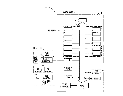
The apparatus 10 of the present invention, as seen in Figure 1, comprises a
planar object imaging assembly 12, also referred to as the sample imaging
assembly, and an associated computerized image processor 14. The planar object
imaging assembly 12, best seen in I~'igures 2, 3 and 4, comprises a light-
tight
housing 20 in which are mounted a sample holding fixture 30, a t7uorescent
illumination assembly 4U, a CCD camera 50, a photographic lens 60 and an
optical filter assembly 70.
The housing 20 comprises a generally rectangular enclosure having a
bottom wall 22I3, side walls 225, a top wall 227 and an interior dividing wall
22D. 1'hc sample holding fixture 30 comprises a generally planar clamping
device
32 which holds a sample S flat in a holding frame 34 in the bottom wall 22B of
the housing 20. l~he clamping device 32 is urged against the frame 34 by a
spring
36. The frame 34 defines a sample plane P.
3
CA 02270935 1999-OS-03
WO 98/20326 PCT/US97/19931
The fluorescent illumination assembly 40 which illuminates the planar
sample S comprises two horizontally mounted 18-inch long FI S/12 cool white
fluorescent tubes, or lamps, 42, 44 which are mounted on the interior dividing
wall 22D approximately 33 centimeters (13 inches) above the plane P of the
sample S and are symmetrically disposed above the center C of the sample S
approximately 40 centimeters ( 16 inches) apart. The lamps 42. 44 arc powered
by
a Mcrcron PX 0648-2 Model G00 controller 46 having a model CI,9 photodetector
accessory 48 which monitors the light output from the lamps and provides a
feedback signal to the controller 46 to produce a precise output light level.
The
walls 22B, 22S, and 22D define a sample illumination chamber 26. The interior
surfaces of the walls of the sample illumination 26 are covered with a high
reflectivity, diffusely reflecting material, such as a flat white paint to
provide a
uniform illumination level to the surface of the sample S.
A ventilator assembly 24 comprising a fan 24P and an air filter assembly
I S 24A is mounted on the top wall 22T to remove heat generated by the lamps
of the
fluorescent illumination assembly 40 and the power supplies and to stabilize
the
temperature of components within the housing. Associated air baffles 24B
distribute air flow around the lamps 42, 44 to provide a more uniform
temperature
profile along the length of the lamps, which results in a more uniform light
output.
Air exits illumination chamber 26 through four one-way air valves 24V. This
airflow also results in a longer useful life of the lamps.
The camera 50, the photographic lens 60, and the filter assembly 70 are
fixedly mounted so that the photographic lens 60 projects an image of the
sample
plane P onto the photodetector ~2 of the CCD camera 50. The lens 60 is mounted
a fixed distance above the sample plane P, in accordance with the focal length
of
the lens. A suitable lens is a Nikon 28 mm focal length, f/2.8 lens which is
mounted about 36 centimeters ( 14.25 inches) above the sample plane P. A lens
hood 62 is employed to reduce stray light collected by the lens 60, which
improves the fidelity of the image with respect to the actual light level
across the
sample.
The optical filter assembly 70 comprises a multiple position turret filter
assembly 72. such as an Uriel model 77379 live position turret, which is
located
between the lens 60 and the CCD camera 50. The turret filter assembly 72 has
five filter holders which respectively contain: 1 ) no filter; 2) a neutral
density
filter having a density of 0.1; 3) a neutral density filter having a density
of 0.3:
4) a neutral density filter having a density of 0.5; 5) a black opaque filter.
An
associated turret control interface module 74, typically a Keitheley Microbyte
model PIO-24 Digital I/O Board, is installed in the computerized image
processor
14 so that the appropriate filter may be selected under software control. 'fhc
4
CA 02270935 1999-OS-03
WO 98/20326 . PCT/US97/19931
purchased turret filter assembly 72 has been modified by machining to reduce
the
thickness dimension of the filter assembly 72 to enable mounting the assembly
72
between the lens 60 and the camera 50 to establish the proper lens-to-
photodetector distance.
The camera 50, such as a Sonv model XC77 video camera, powered by
camera power supply 56, which comprises a CCD photodetector array and
associated control and interface electronics, is mounted vertically with its
CCD
target about 46 centimeters ( 18.125 inches) above the sample plane P. The
photographic lens 60 is typically set with its aperture at f/8. A field of
view of
about 1 1 centimeters by 8 centimeters (4.5 inch x 3.5 inch) on the sample S
is
typically imaged.
Video images generated by the camera 50 are transmitted by a cable to the
computerized image processor 14. The image processor 14 may comprise as
IBM PC compatible computer having the customary Random Access Memory
(RAM) 14R and magnetic storage devices 14M. containing a Matrox Pulsar video
board 100, a Keitheley Microbyte model DAC-02 Digital to Analog (D/A) Board
110, and the Keitheley Microbyte model PIO-24 Digital I/O Board 120 therein.
The computer may typically be controlled using the Windows-NT operating
system, and the video board I00 may be controlled by associated software such
as
the Matrox lmaging Library Version 4Ø 'fhe Analog (D/A) Board 1 10 and the
Digital I/O Board 120 may be controlled by associated software such as the
Blue
Water Systems WinRT device driver.
Video images, typically measuring 640 pixels wide by 480 pixels high, are
digitized by an eight-bit (256 grey levels) analog to digital (A/D) converter
in the
video board I00 and are stored in a suitable memory device. A black reference
level B and a white reference level W, which arc software selectable, arc used
to
control the upper and lower A/D voltages within the video board 100. Thcsc
voltages determine the range of input voltages from the camera 50 which get
mapped to the 256 grey levels (range of 0 to 255) of the A/D converter and
hence
determine the grey level contrast in the digitized image.
Image Contrast L;nhancement
The MdigReference function (part of~ the Matrox Library) allows setting of
the reference levels used to digitize the video signal. In particular, the
black
reference M-BLACK-REF (referred to as I3 here) and the white reierencc
M WHITE_REF (referred to as W here ) are used to select the lower and upper
limit of video signal digitization. Each parameter varies between 0 and 255.
The
relationship between these parameters and camera voltage level are shown in
Figure 8. Varying the parameter B between 0 and 255 selects a particular
camera
5
CA 02270935 1999-OS-03
WO 98I20326 PCT/US97/19931
voltage level V ~ . Similarly, varying the parameter W between 0 and 2S5
selected
a camera voltage level V.,.
The usual digitization relationship is given by line I in Figure 8. Camera
voltage levels between 0 (pedestal level) and 0.7l4 are digitized to grey
levels
between 0 and 255. This corresponds to B=0 and W=Z55. For other values of B
and W the digitization relationship is given by line 1I in Figure 8. Camera
voltage
levels between V ~ and V, are digitized to grey levels between 0 and 255. This
results in increased image enhancement.
~1'he following function relation exists between the software parameters
and the corresponding camera voltage digitization limits:
_ 0.3S7 B
255 (1)
0.357 W
V~ 255 + 0.357 (2)
Preferred values are B - 190 and W = 57 which correspond to V ~ = 0.266
volts and V~ = 0.437 volts, or a camera voltage range of 0.17I volts. The
default
camera voltage range is 0.714 volts (for a 1-volt peak-to-peak video signal).
Thus
image contrast is enhanced by a factor of 4.18 (default camera voltage range
0.174
divided by camera voltage range of 0.171 ).
Dark Signal Correction
The measurement parameter used in the present invention is based on the
ratio of the standard deviation of grey levels to the mean grey level. The
spatial
variation of camera dark signal across an image. although usually small, can
contribute to the measured standard deviation of grey levels. Also, the
measurement parameter will be substantially independent of light level only
when
the dark signal is accounted for and the true image signal is measured. This
section will describe the method derived for correcting the contrast-enhanced
image for dark signal. This method was developed since simply capping the
camera lens results in an image of all zero grey levels as the dark signal
voltages
arc all outside the range V ~ to V~.
From Figure 8 it may be seen that the following function relation exists
between image grey level and camera voltabe:
255 ( )
g«-0.714 Vc 3
6
CA 02270935 1999-OS-03
WO 98/20326 PCT/US97/19931
25S
ge = VZ_V ~ (Vc-V 1 ) (4)
where gu refers to grey levels in the unenhanced image (curve I of Figure 8)
and
gc refers to grey levels in the enhanced image (curve II of Figure 8).
Combining
Eqs. (3) and (4),
gc - 0.714 ~u - 255 V ~ (5)
V2-V I r V2'V 1
Ilq. (5) gives the relationship between grey levels in the enhanced and
unenhanced image, where the enhancement is based on the selection of values
for
V ~ and V~. Thus, if a particular camera voltage level results in an image
pixel
with grey level g~ based on line I in Figure 8, then that pixel will have a
grey level
ge based on line II in Figure 8. In particular, Eq. (5) can be applied to the
grey
levels of the dark signal image.
Thus, the procedure for correcting for dark signal is as follows:
~ Set B=0 and W=255 and sample the dark signal by blocking the
camera lens. Store the dark signal image (with suitable frame
averaging to improve the measurement).
~ For each pixel in the dark signal image, use Cq. (5) to calculate the
corresponding dark signal grey level in the enhanced image and store
these values in a memory buffer of the same size and format as the
rmage.
~ After each enhanced sample image is digitized, subtract the values in
the memory buffer, point by point, from the pixel values in the
enhanced sample image.
As an example, for V ~ = 0.263 volts, V~ = 0.433 volts and an unenhanced
gray level pixel value g" -- 1.5, an enhanced gray level pixel value gc _ -332
results.
Due to variations in electrical components, the actual camera voltage level
limits for digitization, V, and VZ, that correspond to a selection of~B--190
and
W=57 may be different, for any given Matrox Pulsar digitizer board, loom the
expected values calculated using equations ( 1 ) and (2). These camera voltage
level limits are used in equation (5) to calculate the multiplicative and
additive
terms that relate the grey levels in the enhanced and unenhanced images. I:'or
the
rllOSt accurate dark signal correction, the actual values of these
multiplicative and
additive terms should be determined by measurement. Several alternative
procedures can be used.
7
CA 02270935 1999-OS-03
WO 98I20326 PCT/US97119931
One method for refining the dark signal correction is to use a video
oscilloscope, such as the Sony Tektronix 380 NTSC Test Monitor, to measure the
camera voltage corresponding to a particular location in the image. The light
level
is varied to provide a range of camera voltage levels. For each setting of the
light
level. the grey level (average of several neighboring pixels) in the same
image
location being monitored by the video oscilloscope is measured with black
reference level, 13, set to 190 and white reference level) W, set to 57. From
a least
squares lit of the camera voltage data as a function of the grey level to a
straight
line function, one can calculate the camera voltage, V,, corresponding to a
grey
level of 0 and the camera voltage) V,, corresponding to a grey level of 255.
As an
example for a particular Matrox Pulsar board, for B=190 and W-57, equations
(1)
and (2) lead to the following values: V, =0.266 volts and V,=0.437 volts.
Using
the measurement procedure just described. w~e find V,=0.2G7 volts and V,=0.447
volts. Using these values of V, and V, in equation (5), and applying the dark
signal correction method. it is found that paperboard measurements (as
described
below) are substantially independent of the target image average grey level
selected, that is, independent of light Icvci. For example, for a particular
paperboard, the measurements (as described below) varied only between 2.33 and
2.42 for target image average grey levels in the range 75 to 220. This
substantial
measurement independence from light level indicates that the dark signal
correction method is working properly. Without the refinement in the values of
V, and V,) the measurement values differed by about one unit over a smaller
range
of light levels.
Other methods lur refining the dark signal correction involve direct
determination of the multiplicative and additive terms in equation (5) without
knowledge of the V, and V, values. A large number of grey levels are measured
using the same set of pixel locations in two different images, using the same
light
level setting in both cases. In the first, image, B=0 and W=255 are used. In
the
second, contrast enhanced, image, 13=l90 and W=57 are used. The light level
should be set so that there are substantially no pixels at grey levels of 0 or
255 in
either image. Since individual pixel grey levels are used, video frame
averaging
will lead to more accurate results. This procedure results in two sets of grey
levels, g; (enhanced) and g; (unenhanced). where the grey levels for a
particular
value ol' i correspond to the same pixel location in the image. ly doing a
least
squares lit to a straight line function of g, (enhanced) as a function of g;
(unenhanced), one directly obtains from the least squares function the
multiplicative and additive terms in equation (~). A sample that results in a
wide
range of grey levels in each image should be used to obtain a satisfactory
least
squares fit.
8
CA 02270935 1999-OS-03
WO 98/20326 PCTlLTS97/19931
Another method for refining the dark signal correction that involves direct
determination of the multiplicative and additive terms in equation (5) makes
use
of the linear nature of equation (5). That is, the relationship between the
grey
levels at a particular pixel location in the enhanced and unenhanced images
also
holds for the average grey level in a selected region of the enhanced image
and the
average grey level in the same region in the unenhanced image. In the image
with
15
B=0 and W=255, one can select two regions, say, region 1 and region 2, in the
image and calculate, for a given light setting, the average value of grey
level in
each region: G, (unenhanced) and G, (unenhanced). Similarly, in the image with
I3=190 and W=57, one calculates the average grey level in the same two regions
and for the same light level setting: G, (enhanced) and G, (enhanced). Video
frame averaging should be used for each image to improve the accuracy of the
method. Also, the larger the region, the more pixels arc averaged, also
leading to
improved accuracy. The following relationships apply:
G, (enhanced) = a G, (unenhanced) + (3 (6)
G, (enhanced) = a. G~ (unenhanced) + (3 (7)
These two simultaneous equations can be solved for a. and (3 which are
respectively the multiplicative and additive terms in equation (5). A sample
that
results in substantially different values of average grey level between region
1 and
region 2 should be used. Alternatively, one can select more than two regions
and
do a least squares determination of a and ~3 as described above for individual
pixel
grey levels. Averaging over a substantial number of pixels in each region for
the
determination of G;, should lead to improved accuracy over the above described
least squares method based on individual pixel grey levels.
Control of Illumination Level
As may be seen in Figures (iA-6C, the computerized image processor 14 is
programmed to precisely control the light level illuminating the sample S.
This is
accomplished by first setting the analog to digital converter to map the
contrast
enhanced camera voltage range to the full grey level output range. The surface
of
the object is illuminated with the Light source, with the light source being
set to an
initial ouptut level. A digitized frame-averaged image of~thc surface is
created by
first imaging the light reflected ii-om the surface onto the photodctector
array to
create an electrical signal representative of the image. 'hhe electrical
signal is
digitized and frame averaged a predetermined number of times and the frame
averaged representation of the image is stored in the image processor memory.
The average grey level in the image is determined and the illumination level
of the
object is adjusted until the average grey level in the image is at a desired
level.
9
CA 02270935 1999-OS-03
WO 98/Z0326 PCTIUS97JI9931
typically the midpoint of the dynamic range of the analog to digital
converter.
This is done by adjusting the output of tile light source and repeating steps
of
acquiring an image, determining the average grey level and adjusting the
illumination level until the average light level ref3ectcd by the surface of
the object
causes an average grey level in the image of to be within a predetermined
range of
the midpoint of the enhanced contrast dynamic range of the analog to digital
convener. If adjusting the illumination level alone does not result in the
desired
average grey level, then a different optical density filter is selected in
combination
with adjusting the output of the light source until the average light level
reflected
by the surface of the object causes the CCD array to produce an output within
a
predetermined range of the midpoint of the enhanced contrast dynamic range of
the analog to digital converter.
To accelerate the measurement method the initial illumination level is set
by initially setting the light source output level to the level used for the
previous
sample and illumination adjusting step is first performed using a binary
search
method to set Ihc light source output level within a predetermined range of
light
levels. If the desired average grey level is not achieved, the illumination
adjusting
step is then performed using a binary search method to set the light source
output
level over the full range of light levels. if the desired average grey level
is still not
acheived a different optical density f filter is selected and the illumination
adjusting
step is performed using a binary search method to set the light source output
level
over the full range of light levels. If no previous illumination level is
known, the
density of the optical density filter is initially selected at a midrange
density value
and is subsequently reselected if adjustment of the output of the light source
cannot produce an output at the midpoint of the enhanced contrast dynamic
range
of the analog to digital converter.
Analysis Method
With the full 1.2 volt range of A/D voltages selected (Black Reference
level ~- 0, White Reference level = 255, i.e., no enhancement of the image),
the
camera lens is capped, by selecting filter position 5 which contains the
opaque
filter so that no light reaches the CCI~ array. The image produced by the
camera
in the absence of light, known as the "dark response" or "dark current" image,
is
digitized a predetermined number of times (typically l28) and then frame
averaged. Thal is. the corresponding picture elements. or pixels, in each of
the
images are added and then divided by the number of images digitized to produce
an image which represents the average dark current response of the CCD array
and its associated electronics. This so called "average dark current" image is
stored in memory, such as RAM or magnetic storage media, for subsequent use.
CA 02270935 1999-OS-03
WO 98/20326 PCT/US97/19931
- The average dark current image can be used to correct each pixel in the
paperboard image as follows. The average dark current image is first converted
to
a "modified dark current image" to correspond to the contrast range of the
subsequent enhanced sample images in accordance with Equation (5). This
modified dark current image is stored in memory and subsequently subtracted
from each enhanced sample image.
The method of creating the frame-average modified dark current image
comprises the steps of: ( I ) setting the analog to digital converter to map
the full
carrtera voltage range to the full grey level output range; (2) digitizing and
frame
averaging the electrical signal from the CCD photodetector array in the
absence of
light a predetermined number of times to create an averaged dark current
image;
(3) storing the frame-averaged dark current image in the memory; (4) applying
the
transformation factors to create a modified dark current image; (5) storing
the
modified dark current image in the memory.
For each sample, the light level is automatically set so the camera output
voltage to the A/D converter is such that the average grey level in the image
is in
the range 127.5 +/-10. 'The black reference level B and the white reference
level
W reference voltages are set using fixed values: Black = 190, White = 57. This
causes a 0.I7 volt wide A/D voltage window to be centered at the 0.35 volt
center
ND voltage level and results in a grey level contrast enhancement of a factor
of
4.16. The light level produced by the fluorescent lamps is automatically
controlled by the digital to analog (D/A) board 1 10 in the computer to
provide a
reference voltage input to the Mercron controller 46.
Each sample image is frame averaged a predetermined number of times
(typically 64) and the modified dark current image is then subtracted from it
on a
pixel by pixel basis to produce a "dark current corrected image".
Ima a Analysis Algorithm
The image is statistically sampled using a window of a predetermined size
randomly positioned within the image. The window size is selected to
correspond
to the spatial scale of the image features of interest that are observable by
the
human evaluator. Since the analysis window size and the corner coordinates of
the image are known, random numbers specifying the window are generated for
random placement of the analysis window in the image without overlapping the
image border. For paperboard the window is typically a square 31 picture
elements on a side and the number of randomly positioned windows is typicaily
about 500. It should be noted that if the window size is too large, then
shading
due to illumination variations within each window will affect the measurement.
On the other hand, if the window size is too small, then the features oi'
interest,
such as mottle, cannot be detected adequately. Increasing the number of
randomly
CA 02270935 1999-OS-03
WO 98I20326 PCTILJS97/19931
positioned windows will not significantly improve the correlation to human
observations but take longer to run. Using too few randomly positioned windows
will produce "noisier" results and hence poorer correlation to human
observations.
'flhe analysis procedure comprises:
a) Generate a square window of side = 31 picture elements and
randomly place it in the image.
b) Find the mean grey level, gav, and the standard deviation of grey
levels, W,, within the box.
c) Calculate the "variability", v;, within the window:
vi = l00 6y, / gav,
and store this vale in memory;
d) Repeat steps a) to c) 500 times;
e) Calculate the average variability, called the mean variability
factor, Vav, over all windows:
500
vi ,
Vav = 1
500
and store this value in memory.
Re ion of Interest
The system of the present invention has the capability to restrict
measurement on a sample to a region of interest (ROI) in the field of view.
'The
ROI is specified by the user interactively through placement of a cursor box,
which is displayed superimposed on an image of the sample, that is moved and
sized by pressing appropriate keys on the terminal input device to the image
processor 14.
In the standard analysis method, all of the image is measured. Since the
analysis window size and the corner coordinates of the full image are known,
random numbers specifying the window center are generated for random
placement of the window in the image without overlapping the border. The
corner
coordinates of the region of interest are similarly employed so shat the
analysis
window does not overlap the border of the region of interest.
for meaningful results, there should be a lower limit to the size of the
region of interest) which is typically l00 x 100 pixels. Otherwise, the
necessarily
smaller analysis window might be too small to effectively measure the
characteristics of interest of the surface.
12
CA 02270935 1999-OS-03
WO 98/20326 PCT/LTS97/19931
EXAMPLE
The method of the invention was used to characterize a set of 14
paperboard samples. Twelve people took part in a paired-comparison rating test
to visually rank the uniformity of the 14 samples. Each participant was
instructed
to rank the 14 samples according to observed uniformity. For applications such
as
paperboard the mean variability factor is scaled using a fixed scaling factor
for all
samples so that the typical sample has a value in the range of 1 to 10.
Each paperboard sample, which was identified with an arbitrary number
from 1 to 14, was given a rating from 1 (most uniform) to 14 (least uniform)
by
each person. This ranking data was collected. A so-called "trimmed average"
rating and standard deviation of ratings was computed for cach sample. The
"trimmed average" rating was obtained by removing from the ranking data for
each sample the one rating which was most different from all others.
The same 14 samples were analyzed automatically using the apparatus and
the method of the present invention as described above. The results of the
visual
ratings and the results of the method of the present invention are presented
in
Tabie I. The rating obtained using the inventive method was plotted against
the
trimmed average values of visual ratings, as shown in Figure 9. As may be
appreciated from Figure 9 the correlation between the inventive method and the
visual uniformity ratings is quite high, specifically about 0.92.
The repeatability of the inventive method is quite high. For example, ten
images of a typical sample were obtained (without moving the sample) and
analyzed. The average of the mean variability factor was 4.870 and the
standard
deviation was 0.034. This is equivalent to a percent coefficient of variation
(%CV) of 0.71. Thus. it may be concluded that the major limitation in
correlating
the inventive results to the visual ratings is the rather high standard
deviations of
the visual ratings. This may be best appreciated by review of the results
summarized in Table 1.
13
CA 02270935 1999-OS-03
WO 98I20326 PCT/US97/19931
- 'TABLE 1
Visual Rating Standard DeviationInventive Method
8.00 3.08 9.08
4.00 1.89 5.l9
I 0.60 1.40 I 1.99
I I .10 1.54 I 4.48
12.80 0.40 13.92
7.40 1.50 9.56
9.50 I .40 11.31
5.30 2.04 5.l4
7.10 2.G2 9.50
1.90 1.62 4.04
3.50 2.23 G.53
6.70 1.57 7.88
1.70 I .21 3.G7
1.00 I .14 4.57
14