Note: Descriptions are shown in the official language in which they were submitted.
CA 02271028 1999-OS-07
WO 98/23896 PCT/FI97/00697
1
Method for production of conducting element and
conducting element
The present invention relates to a method for produc-
tion of conducting element, which conducting element
consists at least of an elongated and essentially flat
electricity conductive conductor part, such as a band,
a stripe or a like, in which several electric com-
ponents, such as probes, LEDs, resistors and/or the
like bringing out the lighting operation or like
according to the use of the conducting element, are
being attached to one after another in the longitu-
dinal direction, and of a casing part, which conduc-
ting element is being manufactured by arranging the
conductor part and the components existing therewith
when viewed in a cross section totally surrounded by
a casing material forming the said casing part, by
exploiting a continuous manufacturing process, such as
extrusion or like.
In light operated guidance devices, that are meant
particularly e.g. to guide sports performances, it is
previously known to use e.g. lamps, that are connected
one after another to an electric conductor placed
inside a transparent pipe, which guide the athletes'
performance according to a predrafted programme. In
this case, when following the lamps getting lighted
one after another, the athlete may keep the previously
defined speed. The type of traditional solutions
described above are usually based on guidance devices,
that have been put together completely one by one from
separate parts and in which usually bulbs have been
used as lamps, that have been connected in series to
the electric conductor passing through a transparent
pipe. When using the type of guidance devices above
adequate attention must be payed to the tightness of
the casing part, so that water may not enter inside
CA 02271028 2005-O1-17
2
the guidance device, when the same is being used in damp
circumstances or e.g. in a swimming pool.
On the other hand it is known to use also certain type of
electric guidance devices or like, that are manufactured one by
one and that may be used e.g. the way described above when
being coupled to each other one after another. This type of
solutions are usually produced by molding the same inside
transparent plastics, that is why when coupling the guidance
devices to each other completely separate coupling wires must
be used, that must naturally be protected separately as well
when the same are being used e.g. for guiding purposes under
particularly demanding circumstances, such as in inflammable or
the like accommodations. Protection of the intermediate wires
require thus careful installation or auxiliary measures and
components during actual production of the devices on the one
hand a . g . to prevent sparkl ing to the surroundings and on the
other hand to protect the electric wires and actual lighting
devices from water or humidity of the surroundings.
Furthermore e.g. from US Patent 5,496,427, issued
March 5, 1996, it is previously known to produce fully
capsulated lighting strip based on electroluminance by
extrusion. This type of solution, that is purely based on
electroluminance, may be carried out in a totally traditional
way by using merely elongated leads and intermediate stripes,
that continue constant (cf. electric cables). Instead of the
above, with a structure, that is based according to the present
invention on printed circuit board technics, it is possible to
achieve a conducting stripe, that operates particularly
dynamically as well and in which there exists e.g. a light
effect, that moves along the guiding direction. This type of
solution may not in any way be achieved by the stripe according
CA 02271028 2005-O1-17
3
to the above US Patent, that is based on electroluminance,
because it operates by on/off principle only.
On the other hand it is no doubt previously known from
US Patent 5,193,895, issued March 16, 1993 as well to produce
an elongated stripe for lighting purposes. In this patent there
has not been presented, however, particularly a moisture
resistant end product, that may be achieved just by exploiting
extrusion being mentioned above. The type of solution is thus
based on at least two separate parts, in which case moisture
will cause always problems in practice, when the same enters
between the part layers . With this type of solution it is not
either possible to end up to a conducting stripe, that operates
dynamically as described above, but the conducting stripes
enabled by the solution in question always operate by on/off
principle.
Furthermore in EP 760448A, published March 5, 1997, there has
been represented a solution, which is first of all based on two
or more continuous conducting bars passing throughout the whole
conducting stripe, into which LEDs are connected one after
another in the longitudinal direction. The first variation in
the application comprises a solution, which consists of two
elongated conducting bars, into which there has been attached
LEDs, which entirety has been extruded by a suitable plastic
based paste to achieve a built-in elongated conducting stripe.
The other variation in the application is such, that in
addition to the conducting bars a binding stripe is being fed
to the extrusion apparatus, that is unwound from a roll and
that is continuous in the longitudinal direction and on top of
which there exists separate printed circuit boards, in which
the LEDs have been installed. Because in this variation there
has been used conducting bars
CA 02271028 1999-OS-07
WO 98/23896 PCT/FI97/00697
4
as well, that are continuous in the longitudinal
direction, and that are attached to the contact
surfaces existing in those totally separate printed
circuits by means of separate pressing rollers, it is
not possible with the type of solution in question to
achieve such dynamic operation of the conducting
stripe as described above, but instead the solution in
question is further based on traditional on/off use.
In the solution in question the starting point is thus
always such, that the conducting stripe comprises at
least two or more conducting bars passing continuously
from one end to the other end of the same and into
which the LEDs are connected either directly or by
using furthermore a binding stripe, on which the
separate printed circuit boards equipped with LEDs
have been supported. This is why the solution in
question is particularly with a view to manufacturing
technics as well as by the construction of the same
disproportionately complicated, because in connection
with the same there must furthermore be used first of
all conducting bars, continuing in the longitudinal
direction, because of the printed circuit boards, that
are electrically totally separate in respect to each
other, to connect the printed circuit boards and LEDs
existing therewith to each other to achieve at least
a static operation of the conducting stripe.
A method of this invention has an object of providing
a decisive remedy to the above discussed problems and,
thus, of raising substantially the existing prior art.
In order to achieve this object, the method of the
invention is substantially characterized in, that the
electric components of a conducting element, that
enables preferably dynamic use, are being attached
preferably by means of surface mounting technics to an
electric conductor layer, such as to a copper coating
or like of a basic material, that is made of plastics,
CA 02271028 1999-OS-07
WO 98/23896 PCT/FI97/00697
such as polyamide, polyester, polyethylene napthalate
or like, of the conductor part, that is based on so
called printed circuit board technics, whereby the
electric conductor layer continues essentially unin-
5 terruptedly over the whole length of the conducting
element, whereafter the entirety being brought out is
being surrounded by a casing material, that is based
on plastics such as PVC, polyurethane, olefin and/or
like.
The most essential benefits of the method of the
invention include its simplicity and operating re-
liability, which enables significantly more profitable
production when compared to nowadays conducting
elements. The method according to the invention
enables first of all a very low profile, thanks to
which conducting elements according to the invention
may be used e.g. in connection with vinyl floors,
because a guiding element enabled by the method, the
height of which is below 2 mm, may be installed
completely to the same level as the vinyl floor
surface surrounding the same. The method according to
the invention enables that as well, that the conduc-
ting element is water and gas proof, thanks to which
a conducting elements being produced by the method
according to the invention may be used both in damp or
wet rooms/surroundings as well as e.g. in inflammable
surroundings. The method according to the invention
enables a structure, that has a very strong surface,
wherein a conducting element being built e.g. into a
floor does not significantly differ from the original
vinyl floor surrounding the same by its surface
hardness. The method according to the invention is
based on very usual extrusion technics in principle,
which however, when being used in this connection
enables surprising possibilities with a view to
production and final dimensions of the conducting
element to be produced by the method, whereby the
CA 02271028 1999-OS-07
WO 98/23896 PCT/FI97/00697
6
dimensions, shapes and electric characteristics of the
conducting element to be produced may be altered very
easily by making only the necessary simple technical
changes during each working phase. By exploiting the
method according to the invention it is possible to
produce a continuous and flexible conducting element,
that may be stored on roll and in addition to the
above straight bar-like conducting elements naturally
as well. The invention enables furthermore production
of a conducting element, that is secured electrically
by loop principle merely thanks to the conductor part
existing therewith, that has been carried out by
printed circuit board technics. It may be stated in
this connection as well, that the bendability of e.g.
the solution particularly according to the above EP
application may be questionable, because in this
solution the conducting bars are being pressed against
the contact surfaces existing in the conducting
printed circuit boards, in which case when bending the
conducting stripe, the components in question probably
get separated, in which case the electric contact
breaks.
Thanks to the invention it is possible to produce
conducting stripes, that differ from the visual point
of view from all previous solutions as well, by
feeding e.g. differing coating colour layers to the
extrusion apparatus. The colour layers may be of the
same colour as the background, self luminous or e.g.
reflective. It is furthermore possible to arrange e.g.
lences in connection with the colour layers, that are
placed on the LED-component surfaces. In this way it
is possible within a solution according to the inven-
tion to combine intelligently effect of both light and
reflective/self-luminous colour.
CA 02271028 1999-OS-07
WO 98/23896 PCT/FI97/00697
7
The non-independent claims directed to the method said
worth preferred embodiments for the method of the
invention.
The invention relates also to a conducting element to
be produced by the method, that is defined in more
detail in the preamble of the independent claim
directed thereto. The features essentially characte-
ristics for the conducting element are set forth in
the characterizing section of the same claim.
The most significant benefits of the conducting
element according to the invention include simplicity
and operating reliability of production, construction
and use of the same. Particularly use of a so called
continuous manufacturing process, that means so called
extrusion, enables first of all that, that the length
of a conducting element according to the invention may
be even hundreds of meters. The conducting element
according to the invention may be produced as a
completely intergrated structure and e.g. an essen-
tially water and gas tight or moisture resistant
structure. The conducting element according to the
invention may be dimensioned very small, in which case
it may be used e.g. totally built-in with a vinyl
floor, in which case the surface strength and the like
characteristics of the same further correspond essen-
tially to the characteristics of the vinyl floor
surrounding the same. In addition to that, thanks to
the conductor part being carried out electrically by
so called printed circuit board technics, the conduc-
ting element may be produced in a way, that it opera-
tes either statically (no alteration of direction) or
dynamically (with alteration of direction), in which
case the conducting element operates despite the fact,
that some of the electric components of the same stop
functioning for some reason. In case the conducting
element needs to be prepared it may be carried out
CA 02271028 1999-OS-07
WO 98/23896 PCT/FI97/00697
8
simply by changing pieces of the conducting elements,
the length of which correspond one or several sections
of the same, by using e.g. soldering or mechanical
couplings within joints, whereafter the jointing
points may be sealed furthermore with a plastic matrix
corresponding e.g. to the surface of the stripe. The
conducting element according to the invention may thus
be exploited in most heterogeneous connections and
uses, e.g. in public accommodations, ship surroun-
dings, aeroplanes, terminals etc, or for normal
guiding purposes, for emergency or safety lighting
purposes, for control, guidance use, monitoring,
measuring and/or observing purposes etc.; the conduc-
ting element according to the invention may be produ-
ced according to the nowadays LLL-requirements (Low
Location Lighting).
The invention will now be described in more detail
with reference made to the accompanying drawings, in
which
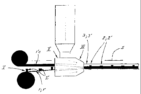
Fig. 1 shows one advantageous general principle of
the method according to the invention and
Figs 2a and 2b
show one advantageous conductor stripe being
produced by the method according to the
invention as a cross-section (fig. 2a) and a
covering band being used in a conductor
stripe according to the invention seen from
above (fig. 2b) .
The invention relates to a method for production of
conducting element, which conducting element consists
at least of an elongated and essentially flat electri-
city conductive conductor part 1; 1', such as a band,
a stripe or a like in which several electric com-
ponents 2; 2', such as probes, LEDs, resistors and/or
CA 02271028 1999-OS-07
WO 98!23896 PCT/FI97/00697
9
the like bringing out the lighting operation or like
according to the use of the conducting element, are
being attached to one after another in the longitu-
dinal direction s, and of a casing part 3. The conduc-
ting element is being manufactured by arranging the
conductor part and the components existing therewith
1 ; 1 ' , 2 ; 2 ' when viewed in a cross section totally
surrounded by a casing material 3' forming the said
casing part 3, by exploiting a continuous manufactu-
ring process, such as extrusion or like. The electric
components 2' of a conducting element, that enables
preferably dynamic use as well, are being attached
preferably by means of surface mounting technics to an
electric conductor layer 1'b, such as to a copper
coating or like of a basic material 1'a, that is made
of plastics, such as polyamide, polyester, polyethyle-
ne napthalate or like, of the conductor part 1', that
is based on so called printed circuit board technics,
whereby the electric conductor layer 1'b continues
essentially uninterruptedly over the whole length of
the conducting element, whereafter the entirety being
brought out is being surrounded by a casing material
3', that is based on plastics such as PVC, polyuret-
hane, olefin and/or like.
Furthermore as an advantageous embodiment, the elect-
ric conductor layer 1'b, such as copper coating or
like of the conductor part, that is made of a con-
tinuous flexible printed circuit board, is being
coated at least by the parts surrounding the electric
components 2' by a covering colour, film 1'c or like
before processing of the casing material 3'.
Furthermore as an advantageous embodiment of the
method with reference particularly to fig., 1 the
electric components 2' are being attached during a
first phase I by surface processing technics to the
flexible conductor part 1' , that is preferably unwound
CA 02271028 1999-OS-07
WO 98/23896 PCT/FI97100697
from a roll, whereafter at least the covering colour,
stripe 1'c or like surrounding at least the electric
components 2' of the conductor part 1' is being
attached to the same during a second phase II and
5 wherein the same is being extruded during a third
phase III by a casing material 3' surrounding the same
essentially overall. Naturally it is possible to vary
the above working stages e.g. in a way, that the
electric components are being placed not until the
10 covering stripe 1'c has been installed etc.
Futhermore as an advantageous embodiment of the
method, during production of the conducting element
co-extrusion is being exploited in other words by
using e.g. three parallel extrusion nozzles particu-
larly for colouring the longitudinal sectors of the
conducting element to be produced alternatively or for
a corresponding purpose.
With reference to the method described above during a
premanufacturing stage the desired lay-out of the
conductor part 1' is being designed and produced.
Thereafter a film is being produced from the lay-out
in question, the size of which is e.g. 1500 mm x 600
mm, whereafter a sieve for the silk-screen is being
produced from the film. After this the protective
colour is being brought by means of the sieve on top
of the electric conductor layer 1'b existing on the
basic material 1'a of the conductor part, whereafter
etching of the conductor part 1' is being carried out,
thanks to which the desired electric lay-out of the
copper surface is achieved.
With the method described above it is possible to
produce several parallel conductor parts to the same
preform in the same connection, which are being cut
from each other after the stages described above and
driven on roll, whereafter the continued process has
CA 02271028 1999-OS-07
WO 98/23896 PCT/FI97/00697
11
been described above. The uninterrupted length of a
continuous printed circuit board being produced e.g.
the way described above and thanks to that the conduc-
ting element as well may be easily even 300 m.
A conducting element according to the invention
consists thus of an elongated electricity conductive
conductor part 1; 1', which has several succesive
electric components 2; 2' that bring out e.g. a
lighting operation, which entirety has furthermore
being surrounded by means of a casing part 3; 3'
protecting the same. The electric components 2' of a
conducting element, that enables at least dynamic use,
are attached preferably by means of surface mounting
technics to an electric conductor layer 1'b, such as
to a copper coating or like to existing on a basic
material 1'a, that is made of plastics, such as
polyamide, polyester, polyethylene napthalate or like,
of the conductor part 1', that is based on so called
printed circuit board technics, whereby the electric
conductor layer 1'b continues essentially uninter-
ruptedly over the whole length of the conducting
element, which entirety is surrounded throughout by a
completely uniform casing material 3', that is based
on plastics, such as PVC, polyurethane, olefin and/or
like.
Furthermore as a particulary advantageous embodiment
particularly to cover the e.g. copper coated outer
surface of the conductor part 1', that is made of a
continuous flexible printed circuit board, on top of
the same there is arranged a covering colour film 1'c
or like at least on the parts surrounding the electric
components 2'. Particularly when a separate covering
film is being used e.g. as shown in fig. 2b, in which
there has been prepared during a premanufacturing
stage openings at points corresponding the places of
the components 2'a, 2'b to be connected to the conduc-
CA 02271028 1999-OS-07
WO 98/23896 PCT/FI97/00697
12
for part 1', the solution is advantageous in such
respect, that by using a suitable material thickness
therewith it is possible to even the outer surface of
the conductor part particularly with a view to the
extrusion stage. Small alterations in heigth on the
outer surface of the conductor part 1' may be eli-
minated during manufacturing e.g. by altering drawing
speed and/or extrusion pressure during extrusion.
Furthermore as an advantageous embodiment in connecti-
on with a conducting element, that is meant to be
installed particularly built-in with a vinyl floor,
the total thickness v of the conducting element is at
the most 2 mm, whereby the thickness v of the casing
material 3' of the lowermost part of the conductor
part 1' is preferably 0,1 - 0,3 mm.
As a particularly advantageous embodiment with refe-
rence particularly to the general principle of the
method shown in fig. 1, the conducting element has
been produced from a flexible conductor part, in which
case the produced conducting element may be furthermo-
re stored on roll. When exploiting in other respects
nowadays technology existing completely already, it is
possible to produce e.g. conducting element according
to the invention, the breadth w of which is e.g.
between 5-1500 mm. The mentioned values may not in any
way limit the solution being exploited in this connec-
tion, because it is possible to achieve smaller/grea-
ter dimensions than presented above by very simple
arrangements.
Furthermore as an advantageous embodiment the conduc-
tor part 1' of the conducting element has been formed
of at least two or several printed circuit boards or
printed circuit board layers, that are electrically
isolated from each other placed on one another. It is
thus possible to produce e.g. a conducting element as
CA 02271028 1999-OS-07
WO 98/23896 PCTIFI97/00697
13
well, in the printed circuit board of which there
exists mutually differing and electrically isolated
copper coatings on both opposite surfaces of the same.
This type of embodiments have not been shown in the
drawings, because they may be easily constructed in
practice as embodiments, that are electrically isola-
ted from each other, by arranging the coating conduc-
ting electricity only on one side of each printed
circuit board layer. With the type of solutions it is
possible to lead/transmit e.g. separate groups, canals
passing in different kinds of buildings. In this way
it is also possible to increase information being
transmitted by the conductor stripe without however
essentially increasing the total thickness of the
conducting element. Furthermore the electric com-
ponents of the conducting element may comprise LED-
matrices being placed one after another in the longi-
tudinal direction as well, e.g. to form letters,
figures or text. In addition to that multicolour LEDs
may be used in certain kinds of embodiments as the
electric components, in which case depending on the
situation the colour of the LEDs is most suitable to
each operating purpose (green/red etc.).
It is obvious, that the invention is not limited to
the above described or discussed embodiments, but it
can be subject to even major modifications within the
context of the basic concept. As explained above it is
thus naturally possible to produce elongated stiff
structures as well apart from the type of flexible
conducting elements as explained above. It is natural-
ly possible to exploit e.g. base rods made of plastics
in connection with the type of flexible structures as
described above as well, when the conducting elements
are being used e.g. in connection with textile floors
or by exploiting aluminium or steel structured base
rods when the same are being used particularly in
connection with stone floors, in which it is not
CA 02271028 1999-OS-07
WO 98/23896 14 PCT/FI97/00697
possible to make recessions or grooves, so that the
conducting element could be built in the floor. It is
naturally obvious as well, that it is advantageous to
produce the conducting element according to the
invention in a way, that it has parts of certain
length, according to which the conducting element may
be cut and repaired afterwards. The method according
to the invention,may be exploited in such a way as
well, that instead of coating or colouring of the
conductor stripe, in connection with the extrusion a
casing material is being used, the desired parts of
which are a . g . opaque and from certain points further-
more transparent or see-through. Thanks to the moistu-
re resistant structure enabled by the invention it is
naturally important to pay attention to the moisture
isolation of the mutual joints of e.g. the conducting
elements to be coupled to each other one after another
or of conducting elements and control unit/power
source, by using a joint material, that is suitable in
this connection e.g. castable polyurethane.