Some of the information on this Web page has been provided by external sources. The Government of Canada is not responsible for the accuracy, reliability or currency of the information supplied by external sources. Users wishing to rely upon this information should consult directly with the source of the information. Content provided by external sources is not subject to official languages, privacy and accessibility requirements.
Any discrepancies in the text and image of the Claims and Abstract are due to differing posting times. Text of the Claims and Abstract are posted:
| (12) Patent Application: | (11) CA 2271108 |
|---|---|
| (54) English Title: | ARRANGEMENT IN A SUBSCRIBER LINE INTERFACE CIRCUIT |
| (54) French Title: | CONFIGURATION DE CIRCUIT D'INTERFACE DE LIGNE D'ABONNE |
| Status: | Deemed Abandoned and Beyond the Period of Reinstatement - Pending Response to Notice of Disregarded Communication |
| (51) International Patent Classification (IPC): |
|
|---|---|
| (72) Inventors : |
|
| (73) Owners : |
|
| (71) Applicants : |
|
| (74) Agent: | MARKS & CLERK |
| (74) Associate agent: | |
| (45) Issued: | |
| (86) PCT Filing Date: | 1997-11-06 |
| (87) Open to Public Inspection: | 1998-05-22 |
| Examination requested: | 2002-10-22 |
| Availability of licence: | N/A |
| Dedicated to the Public: | N/A |
| (25) Language of filing: | English |
| Patent Cooperation Treaty (PCT): | Yes |
|---|---|
| (86) PCT Filing Number: | PCT/SE1997/001857 |
| (87) International Publication Number: | SE1997001857 |
| (85) National Entry: | 1999-05-07 |
| (30) Application Priority Data: | ||||||
|---|---|---|---|---|---|---|
|
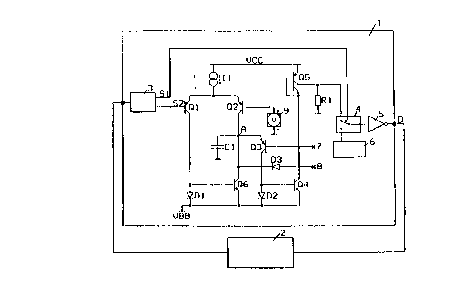
A control processor (2) is connected to a subscriber line interface circuit
(1) to, on the one hand, control the operating mode of the line interface
circuit (1) and, on the other hand, monitor, via a detector output terminal
(D) of the line interface circuit (1), the status of a line connected to the
line interface circuit (1). The control processor (2) is adapted to control
the line interface circuit (1) to, on the one hand, ensure, at a first point
of time, that its detector output terminal (D) is in a first signal state and,
on the other hand, at that first point of time, initiate measurement of the
line voltage. The line interface circuit (1) is adapted, at a second point of
time, to bring the detector output terminal (D) to a second signal state after
a time interval whose length in a predetermined manner is proportional to the
measured line voltage, and the control processor (2) is adapted to convert the
time interval during which the detector output terminal (D) of the line
interface circuit (1) is in the first signal state, to a voltage value
corresponding to the line voltage.
Un processeur de commande (2) est connecté à un circuit d'interface de ligne d'abonné (1) d'une part pour commander le mode de fonctionnement du circuit d'interface de ligne (1) et d'autre part pour surveiller, par l'intermédiaire d'une borne de sortie de détection (D) du circuit d'interface de ligne (1), le statut d'une ligne connectée au circuit d'interface de ligne (1). Le processeur de commande (2) est conçu pour commander le circuit d'interface de ligne (1), d'une part, afin de faire en sorte que, à un premier moment, sa borne de sortie de détection (D) soit dans un premier état de signal et, d'autre part, à ce premier moment, démarrer la mesure de la tension de ligne. Le circuit d'interface de ligne (1) est conçu pour faire passer la borne de sortie de détection (D) dans un deuxième état de signal, à un deuxième moment, après un intervalle de temps dont la longueur est, de manière prédéterminée, proportionnelle à la tension de ligne mesurée. Le processeur de commande (2) est conçu pour convertir l'intervalle de temps, pendant lequel la borne de sortie de détection (D) du circuit d'interface de ligne (1) est dans le premier état de signal, en une valeur de tension correspondant à la tension de ligne.
Note: Claims are shown in the official language in which they were submitted.
Note: Descriptions are shown in the official language in which they were submitted.
2024-08-01:As part of the Next Generation Patents (NGP) transition, the Canadian Patents Database (CPD) now contains a more detailed Event History, which replicates the Event Log of our new back-office solution.
Please note that "Inactive:" events refers to events no longer in use in our new back-office solution.
For a clearer understanding of the status of the application/patent presented on this page, the site Disclaimer , as well as the definitions for Patent , Event History , Maintenance Fee and Payment History should be consulted.
| Description | Date |
|---|---|
| Inactive: IPC from MCD | 2006-03-12 |
| Inactive: IPC from MCD | 2006-03-12 |
| Application Not Reinstated by Deadline | 2004-11-08 |
| Time Limit for Reversal Expired | 2004-11-08 |
| Deemed Abandoned - Failure to Respond to Maintenance Fee Notice | 2003-11-06 |
| Letter Sent | 2002-12-02 |
| All Requirements for Examination Determined Compliant | 2002-10-22 |
| Request for Examination Received | 2002-10-22 |
| Request for Examination Requirements Determined Compliant | 2002-10-22 |
| Inactive: Cover page published | 1999-07-28 |
| Inactive: First IPC assigned | 1999-06-23 |
| Letter Sent | 1999-06-09 |
| Inactive: Notice - National entry - No RFE | 1999-06-09 |
| Application Received - PCT | 1999-06-07 |
| Application Published (Open to Public Inspection) | 1998-05-22 |
| Abandonment Date | Reason | Reinstatement Date |
|---|---|---|
| 2003-11-06 |
The last payment was received on 2002-10-31
Note : If the full payment has not been received on or before the date indicated, a further fee may be required which may be one of the following
Patent fees are adjusted on the 1st of January every year. The amounts above are the current amounts if received by December 31 of the current year.
Please refer to the CIPO
Patent Fees
web page to see all current fee amounts.
| Fee Type | Anniversary Year | Due Date | Paid Date |
|---|---|---|---|
| Registration of a document | 1999-05-07 | ||
| Basic national fee - standard | 1999-05-07 | ||
| MF (application, 2nd anniv.) - standard | 02 | 1999-11-08 | 1999-11-01 |
| MF (application, 3rd anniv.) - standard | 03 | 2000-11-06 | 2000-11-02 |
| MF (application, 4th anniv.) - standard | 04 | 2001-11-06 | 2001-10-23 |
| Request for examination - standard | 2002-10-22 | ||
| MF (application, 5th anniv.) - standard | 05 | 2002-11-06 | 2002-10-31 |
Note: Records showing the ownership history in alphabetical order.
| Current Owners on Record |
|---|
| TELEFONAKTIEBOLAGET LM ERICSSON |
| Past Owners on Record |
|---|
| HANS ERIKSSON |

