Note: Descriptions are shown in the official language in which they were submitted.
CA 02272012 1999-OS-11
1
COMMUNICATION PLUG HAVING LOW COMPLEMENTARY
CROSSTALK DELAY
BACKGROUND OF THE INVENTION
The present invention relates generally to the field of modular communication
plugs and, more particularly, to the generation of complementary crosstalk in
a
communication plug such that performance with connector jacks is optimized.
Telecommunications and data transmission systems have evolved in recent years
to accommodate the increasing demand for high speed, multi-media services.
Accordingly, higher and higher frequencies are being transmitted across
network
to infrastructure originally designed for lower throughput. Although present
day cables
and wiring, can, theoretically, handle such increased frequencies and traffic
volume, the
wiring paths themselves become, in effect, antennae that both radiate and
receive
electromagnetic radiation, thereby creating crosstalk problems. c:rosstalk is
particularly problematic in systems incorporating multiple wire pairs.
Unfortunately,
the plugs and jacks that are most commonly used in interconnecting cables and
hardware, such as distribution modules, generally include up to eight wires
(four wire
pairs) that are necessarily oriented both parallel and close together, a
condition that
leads to excessive crosstalk, even over short distances, and which is
exacerbated as the
frequency of the signals or the data rate is increased.
2o Various techniques have been used for reducing crosstalk in communication
plugs and cables, such as shielding individual pairs, helically winding
twisted pairs, or,
where possible, increasing the physical separation of one pair from another.
The
crosstalk problem, however, cannot be managed through a simple minimization or
reduction approach. While it may be desirable in future applications to
eliminate
virtually all crosstalk in a communication plug, legacy systems (i.e., current
jacks)
require a predetermined amount of crosstalk in the plug for optimum
performance.
Legacy jacks are engineered to compensate for crosstalk in the communication
plug;
CA 02272012 1999-OS-11
2 Adriaenssens 6-31-8-7-7-10
thus, a well designed plug should generate crosstalk that is complementary to
that used
in the jack so the combination of the two crosstalk signals cancel each other
out.
For the crosstalk signals generated in the plug and the jack or connector to
be
completely complementary, they should be of equal magnitude and be 180°
out of
phase with one another. The crosstalk signals generated in the plug and the
jack are
separated initially by some defined distance, which results in a propagation
time delay
before the signals combine. This propagation delay can cause the phase
difference
between the two crosstalk signals to shift from the desired 180° to
some other value,
which prevents the plug and jack crosstalk signals from completely canceling
one
1o another out. It is therefore desirable, that the complementary crosstalk in
the plug be
generated proximal to the jack to minimize the propagation delay for the
complementary crosstalk signals.
Thus, what is sought is a communication plug having engineerable parameters
that can be modified to generate a desired level of crosstalk to adapt to the
compensating crosstalk characteristics of a jack or connector in which the
plug will be
used. Preferably, the communication plug generates the crosstalk near the plug
jack
interface to minimize the propagation delay between the crosstalk signals from
the
respective components.
SUNINIARY OF THE INVENTION
2o Certain advantages and novel features of the invention will be set forth in
the
description that follows and will become apparent to those skilled in the art
upon
examination of the following or may be learned with the practice of the
invention.
The present invention is generally directed to a communication plug that
generates crosstalk that complements the compensating crosstalk in a legacy
jack or
connector. In a preferred embodiment, the communication plug comprises a
dielectric
carrier on which a plurality of electrical conductors are disposed. Each
conductor is
configured to wrap around a first end of the carrier thereby forming a series
of adjacent
CA 02272012 1999-OS-11
3
inductive loops. Crosstalk is generated between the conductors as a result of
the fields
created from current flow through the inductive loops.
According to an aspect of the invention, the complementary crosstalk generated
in the plug can be fixed to a desired level by modifying certain engineerable
parameters
such as the direction that each conductor loops around the end of the carrier.
Other
engineerable parameters include the length of the inductive loops, the design
of the
dielectric carrier, and the type of material from which the carrier is made.
Advantageously, the inductive loops are positioned in the nose or front region
of the
plug where the conductors engage the jack spring wires or terminals. As a
result,
to propagation delay between the crosstalk signals generated in the plug and
the jack or
connector is minimized thus enhancing the effectiveness of the crosstalk
compensation
design.
The communication plug according to the present invention can optionally
include means for complementing the impedance profile of a jack or connector.
By
matching the impedance of the plug and jack system to that of the nominal
impedance
of the cable, signal loss due to reflections, and unwanted noise due to said
reflections,
are minimized. In a preferred embodiment, the impedance matching means
comprises
parallel plates disposed on certain conductors to create a capacitance within
the plug.
BRIEF DESCRIPTION OF THE SEVERAL VIEWS OF THE DRAWINGS
2o Other features of the present invention will be more readily understood
from the
following detailed description of specific embodiments thereof when read in
conjunction with the accompanying drawings, in which:
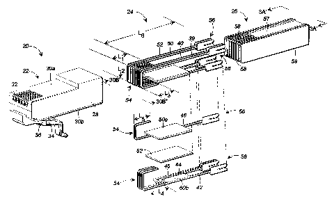
FIG. 1 is an exploded isometric view of a communication plug according to the
present invention;
FIG. 2 is an exploded isometric view of the communication plug of FIG. 1
illustrating the underside of the plug;
CA 02272012 1999-OS-11
r .
4 Adriaenssens 6-31-8-7-7-10
FIG. 3A is an elevation view of the communication plug of FIG. 1 taken along
line 3A'-3A' of FIG. 1 and illustrating the arrangement of the insulation
displacement
connector (IDS) ends of the conductors; and
FIG. 3B is an elevation view of the communication plug of FIG. 1 taken along
line 3B'-3B' of FIG. l and illustrating the arrangement of the conductors at
the nose or
front end of the plug.
DETAILED DESCRIPTION OF THE PREFERRED EMBODIMENT
While the invention is susceptible to various modifications and alternative
forms, a specific embodiment thereof is shown by way of example in the
drawings and
1o will herein be described in detail. It should be understood, however, that
there is no
intent to limit the invention to the particular form disclosed, but on the
contrary, the
invention is to cover all modifications, equivalents, and alternatives falling
within the
spirit and scope of the invention as defined by the claims.
Referring now to FIGS. l and 2, a communication plug 20 embodying the
principles of the present invention is shown to comprise a housing 22, a
plurality of
conductors 24, and a conductor carrier 26. Housing 22, which is typically made
from a
suitable dielectric material such as plastic, comprises a substantially hollow
shell having
side walls 28 and upper and lower walls 30a and 30b respectively. Upper wall
30a
includes a plurality of slots 32 at the nose or front end of the housing for
receiving jack
2o springs contained in a wall terminal block or other connector containing a
jack interface
with which the plug of the invention is designed to mate. The number of slots
32 and
the dimensions of housing 22 are dependent on the number of conductors to be
terminated and/or connected and the shape of the jack in the terminal block.
For most
applications, the general shape of housing 22 remains consistent with the
number of
slots and the overall width thereof varies in relation to the number of
conductors.
To secure communication plug 20 in a jack, housing 22 includes a resilient
latch
34 extending from lower wall 30b. Because latch 34 is secured to housing 22 at
only
CA 02272012 1999-OS-11
one end, leverage may be applied to the latch to raise or lower locking edges
36. When
housing 22 is inserted into a jack, pressure can be applied to latch 34 to
raise locking
edges 36 for easy entry. Once housing 22 is seated within the jack, latch 34
can be
released causing locking edges 36 to be held behind a plate forming the front
of the
5 jack, which is generally standard on such jacks, thereby securing the
connection.
Similarly, housing 22 can be released via leverage on latch 34 to free locking
edges 36
from behind the jack plate so that housing 22 can be removed.
The internal components of communication plug 20 include conductors 24 and
conductor carrier 26. Carrier 26 is made from a dielectric material, such as
plastic, and
1o has channels and depressions formed thereon to receive the individual
conductors 24.
The arrangement of conductors 24 once assembled in carrier 26 is shown best in
FIGS.
3A and 3B. FIG. 3A depicts the )DC ends of conductors 24 extending from the
rear or
back end of carrier 26. Similarly, FIG. 3B depicts the jack spring interface
ends of
conductors 24 arranged at the nose or front of carrier 26. The principles of
the
invention are disclosed as applied to an eight wire communication plug. Those
skilled
in the art will appreciate that the concepts taught herein can be applied to
plugs
terminating cables carrying any number of conductors or wires in which
crosstalk is
generated in both the plug and the jack or connector. Nevertheless, eight wire
cables
are generally configured as four wire pairs. These wire pairs map into
conductors 24 as
2o shown in FIGS. 3A and 3B: pair I comprises conductors 44 and 46
(hereinafter pair
44-46); pair II comprises conductors 38 and 40 (hereinafter pair 38-40); pair
III
comprises conductors 42 and 48 (hereinafter pair 42-48); and pair IV comprises
conductors 50 and 52 (hereinafter pair 50-52). It should be noted that the
pair
numbering used herein is for example only. The principles of the present
invention
apply to any numbering scheme or pair assignment. Pairs 42-48 and 44-46
generally
have the largest amount of crosstalk generated in plug 20 because the
conductors in
pair 42-48 must be split to straddle the conductors of pair 44-46 (see FIG.
2B), which
is a common standard in eight conductor plugs. As discussed hereinbefore, the
crosstalk is generated not only between pairs 44-46 and 42-48, but between all
pair
CA 02272012 1999-OS-11
Adriaenssens 6-31-8-7-7-10
combinations, and should be engineerable to complement the crosstalk generated
in the
jack or connector. Thus, communication plug 20 should have some means for
fixing
the amount of crosstalk generated between each pair combination.
Returning to FIGS. 1 and 2, conductors 24 are each shown to have a loop end
54 and an IDC end 56. Loop ends 54 are received in channels defined in the
nose or
front of carrier 26 by guide walls 58. IDC ends 56 rest at the rear or back
end of
carrier 26 with each contact being bifurcated to comprise dual, elongated
prongs
forming a narrow slot therebetween. The tips of the dual prongs are beveled to
facilitate reception of an insulated wire from the cable and the inner edges
of the prongs
1o have sharp edges for cutting through the conductor insulation. Loop ends 54
are the
primary means by which complementary crosstalk is engineered in communication
plug
20. It can be seen that loop ends 54 are positioned close together such that a
series or
array of inductive loops is formed whereby electrical alternating current flow
in one
loop generates an electromagnetic field that triggers current flow in
neighboring loops.
~5 The direction of the electromagnetic field and the direction of the current
flow are
related. Moreover, loops 54 are located in substantially parallel planes with
one
another, which produces the greatest inductive interaction. Also, the
proximity of the
conductors in this region gives rise to capacitance between the conductors,
which
generates crosstalk.
2o Thus, plug designers have several engineerable parameters at their disposal
in
the region defined by lengths Ll, L2, and L3, which comprise loops 54, to
adjust the
amount of complementary crosstalk generated. The first parameter is selection
of
which conductors run along the top 57 of earner 26, and which run along the
bottom
59. As shown in FIGS I and 2, conductors 38, 40, 50, and 52 (i.e., pairs II
and I~
25 extend along the top 57 of carnet 26 with ends 54 looping around the nose
and
terminating on the bottom 59 of carrier 26. Conversely, conductors 44, 46, 4z,
and 4~
(i.e. pairs I and III) extend along the bottom 59 of earner 26 with ends 54
looping
around the nose and terminating along the top 57 of carrier 26. In conductors
38, 40,
50 and 52, the current runs along the top 57 of the carrier 26 only, and in
conductors
CA 02272012 1999-OS-11
7
44, 46, 22, and 48 the current runs along the bottom 59 of carrier 26 and up
the front
or nose of carrier 26 (i.e., along length L2). As discussed in the foregoing,
the
electromagnetic field, and hence the inductively coupled crosstalk, is
directly related to
the current flow in the conductor. Also, the capacitive coupling is related to
the
proximity of the respective conductors to one another. Hence, through careful
selection of the locations of the conductors, a near optimum crosstalk
conduction can
be achieved, which can be further optimized by selection of the other
parameters. One
particular set of conductor locations is disclosed herein as a preferred
embodiment. It
should be understood that implementations using other sets of conductor
locations in
to which crosstalk conduction is optimized as taught hereafter are within the
spirit of the
present invention.
Second, the length L4 over which the inductive loops of pairs 44-46 and 42-48
are closely spaced can be adjusted. This has a direct effect on the amount of
inductively coupled crosstalk and capacitively coupled crosstalk generated
between
pairs 44-46 and 42-48 in the loop 54 region (i.e., along lengths Ll, L2, and
L3). Third,
the length LS of the non-current carrying extensions of all eight conductors
can be
varied independently to alter their capacitive coupling. A fourth parameter
for
managing crosstalk in communication plug 20 is the design of carrier 26 and
the
material from which Garner 26 is made. Carrier 26 is generally made from a
dielectric
2o material such as plastic, which increases capacitance, and hence crosstalk
between
conductor pairs. It is desirable to generate substantially all of the
complementary
crosstalk at the nose or front of communication plug 20 and to minimize
crosstalk in
the body of the plug to minimize the propagation delay between the
complementary
crosstalk in the plug and the compensating crosstalk from the jack or
connector. Thus,
carrier 26 is generally designed to maximize the electrical segregation of
conductors 24
in the region identified as L6 in FIG. 1, which begins with the termination of
loop ends
54 and extends to the IDC ends of conductors 24.
CA 02272012 1999-07-26
t
8
It will be appreciated by those skilled in the art that the present invention
generates complementary crosstalk in the communication plug predominantly
along the
region defined by lengths Ll, L2, and L3 through inductive loop ends 54, and
through
capacitive unbalance in this region. Advantageously, the complementary
crosstalk is
generated at the junction where communication plug 20 engages the jack springs
of a
jack or connector thus minimizing any signal propagation delay and
facilitating the
elimination of crosstalk in the system with proper compensation techniques.
In addition to generating the appropriate complementary crosstalk, the mated
combination of plug 20 and its jack is also required to meet certain return
loss
1o requirements as prescribed in standards set forth by the International
Electrotechnical
Commission (IEC) and Telecommunication Industry Association (TIA). These
standards effectively place limits on the impedance of the plug. Furthermore,
it is well
known that to minimize return loss of a mating communication plug and a jack
or
connector, the impedance of the connection point should match that of the
cabling it is
used with. Accordingly, capacitive plates 60a and 60b are designed into
conductors 48
and 42 respectively (i.e., pair 42-48) to manage the impedance of the mated
combination of the jack or connector and plug 20, and to comply with IEC and
TIA
standards. Dielectric spacer 62, which is typically made from plastic having a
high
dielectric constant, separates plates 60a and 60b to form a capacitor.
Dielectric spacer
62 can be frictionally held between plates 60a and 60b and/or secured with an
adhesive.
The bottom 59 of carrier 26 includes a recessed region 64 for receiving plates
60a, 60b,
and spacer 62. Other means can also be used for separating plates 60a and 60b.
For
example, it is common to use a dielectric adhesive tape on the underside of
plate 60a to
fulfill the role of spacer 62. The size of plates 60a and 60b, the size of
dielectric spacer
62, and the type of material spacer 62 is made from can all be modified to
adjust the
capacitance level. Moreover, plates 60a and 60b can alternatively be designed
from
discrete components and placed in proximity to the desired conductors v~iith
proper
support from carrier 26.
f CA 02272012 1999-OS-11
9
Note that dielectric spacer 62 causes conductor 48 to be offset slightly from
the
remaining conductors in pairs 44-46 and 42-48 as shown in FIGS. 2 and 3A. The
skilled practitioner will recognize that alternative means can be used to
adjust the
impedance and capacitance developed in communication plug 20 such as
alternative
plate designs, routing the conductors close together to form capacitive
regions, and
designing resistive regions in conductors 24, which could change the spatial
configuration of both conductors 24 and/or carrier 26.
The principles of the present invention have been illustrated herein as
embodied
in a communication plug for a mufti-wire cable. From the foregoing, it can
readily be
1o seen that the communication plug can be engineered during the design
process to
generate complementary crosstalk to match the characteristics of the jack or
connector
to which the plug will be mated. Most importantly, however, the complementary
crosstalk is generated at the nose or front of the plug where the conductors
engage the
jack springs in the jack or connector thus minimizing any signal propagation
delay and
maximizing the effectiveness of the crosstalk compensation design. Several
engineerable parameters are identified that can be adjusted during the design
and
manufacturing phases of the plug to fix the complementary crosstalk level.
In concluding the detailed description, it should be noted that it will be
obvious
to those skilled in the art that many variations and modifications can be made
to the
2o preferred embodiment without substantially departing from the principles of
the present
invention. All such variations and modifications are intended to be included
herein
within the scope of the present invention, as set forth in the following
claims.