Note: Descriptions are shown in the official language in which they were submitted.
CA 02272202 2005-06-14
-1-
TITLE
DRIVE WITH HIGH OUTPUT IN FAILED MODE
BACKGROUND OF THE INVENTION
I. Field of the Invention
This invention relates to a drive and specifically a drive and a method for
operating a variable drive such as a variable-speed motor drive system.
II. Description of Prior Art
Variable-output drives traditionally are used in industry to provide variable
electric power to AC motors. These same drives can be used in other
applications not
related specifically to motors but where a variable-output voltage or
frequency is
desired. Typical drives have an AC input power source and some type of
conversion
apparatus, usually using solid-state devices, for converting the fixed AC
input voltage
into a variable-voltage and/or variable-frequency output. One such type of
drive is
described in U.S. Pat. No. 5,625,545. That patent describes a power supply
used as a
drive which utilizes a number of power cells arranged to produce a three-phase
AC
output. Such multiple power cells in series can be utilized to provide higher
voltage
outputs than would be available with only a single cell. However, should a
given cell in
a series arrangement fail during operation, that current path can become open-
circuited,
rendering the entire drive inoperable. In many applications, especially
industrial
applications utilizing variable-speed drives, it is
CA 02272202 1999-OS-19
-2-
desirable to continue to operate in a reduced mode when a single cell fails.
One method
to do such a reduced operation is to short out the damaged or failed cell.
This can then
result in an unbalanced output, in that the leg having the shorted cell must
operate at
less than full voltage. Such operation can create imbalanced line conditions
and be
damaging to load elements. Therefore, when a cell fails in a series
arrangement, it is
usually desirable to permit operation at a reduced voltage or speed by
shunting out an
equal number of cells in each of the other legs. While the output from such a
drive
having shunted cells in each leg is reduced, it does permit the dri~,~e to
operate at a
reduced voltage or speed. Often times such reduced operation is highly
desirable so
that the process being controlled by the drive can continue until it is
convenient to shut
down for repairs. In addition, it may be desirable to operate the drive at a
reduced-
voltage condition so as to maintain a desired minimum level of production.
Typically,
when a drive having multiple converters arranged in series l.as a failure, the
output
voltage and power available is reduced proportional to the~ratio of the number
of
unfailed cells in a given leg divided by the number of total cells in such
leg. As an
example, if one of the cells in the aforesaid patent, such as power cell A,
were to fail,
typically power cells A~, B, and C1 would be shunted by appropriate bypass
circuitry.
Such circuitry is shown in Figure 9 of the 5,625,545 patent. When operating
under
such bypass condition, the output of the three-phase drive at references 22,
25 and 24 is
proportionally reduced by one-third. In such an operating condition, the
output voltage
available to the motor would only be 66% of the full voltage. In such a
condition, the
motor would only be able to reach approximately two-thirds of its rated speed.
In many
CA 02272202 1999-OS-19
-3-
applications being able to reach even 66% of rated speed in a failed cell mode
is
desirable. However, it still represents a substantial reduction in the output
speed and
power available from the drive. When multiple power cells or converters are
used in
series, the total power delivered to the load is usually supplied generally
equally by all
the power cells. Thus in the example above when one of nine cells fails, 89%
of rated
power should still be available. By shunting out or bypassing two operational
power
cells such as B1 and C~ in the example, these power cells can no longer
contribute to the
output power available to the load. It would be very desirable, then, to
optimize the
output voltage and power available to the load during a failed cell condition.
The
invention provides for an apparatus and a method that permits operation during
a failed
mode at a power output that utilizes all of the cells or converters that are
operational.
SUMMARY OF THE INVENTION
The invention is directed to a method of operating a multiphase=power supply
that has a plurality of cells or converters connected in series in each of a
plurality of
legs. This results in each leg having a leg voltage equal to the sum of
connected cells in
such leg. In addition, the power supply has a line-to-line voltage output
between the
terminal ends of each pairs of legs. This invention applies to loads that are
not
connected to the common leg junction, but only to the end points of the legs,
so that
only the line-to-line output voltage appears on the load. During a failed
condition in
which any one or number of cells have failed in any of the legs, the line-to-
line voltage
output is maximized. This is done by detecting failed cells in any of the legs
and
forming a current path around such failed cell by an electrical bypass. As a
result no
CA 02272202 1999-OS-19
-4-
voltage component from the failed cell is included within the leg in which it
previously
was connected. The outputs of the unfailed cells are controlled so as to
maximize the
line-to-line voltage in the output of the power supply so that their
magnitudes are
generally equal. By so regulating their outputs, the line-to-line phase
voltages of the
output of the power supply can be balanced. In a three-phase output supply
without
failed cells, balanced voltage is maintained by having a 120° phase
relationship
between the leg output voltages. The line-to-line phase balance can be
restored by
adjusting the leg-to-leg phase relationship between the respective legs when
failed cells
are detected. Circuitry is provided to implement a method for reducing the
peak
voltage demands between legs. Voltage command signals can be generated to
provide
peak voltage reduction, and such signals can be modified to compensate for the
detection of failed cells. The modification can be a gain control using a gain
which is
proportional to the ratio of the total number of cells in the leg (including
failed cells)
divided by the number of active cells (not bypassed) in the leg. ~ he
invention is
particularly adapted to pulse width modulated serial converters in each leg.
The result
is balanced line-to-line output from the power supply and full utilization of
each
unfailed cell in the system.
DESCRIPTION OF THE DRAWINGS
Figure 1 a is a diagram showing the power circuitry of an embodiment having
five power cells in each leg of a three-phase drive.
Figure 1 b is a diagrammatic representation showing the converter circuitry of
an
embodiment of one cell such as those shown in Figure 1 a.
CA 02272202 1999-OS-19
-$-
Figure 1 c is a diagrammatic representation of an embodiment of a control
signal
scheme that could be used to control a five-cell-per-leg drive such as shown
in
Figure 1 a.
Figure 1 d shows four alternative embodiments of a cell bypass.
Fig,~re 2 is a voltage diagram of a typical array of five cells connected in
series
in each leg of a three-phase output.
Figure 3 is a diagrammatic representation of voltage in an array similar to
that
shown in Figure 2 but having two failed cells out of leg A.
Figure 4 (Prior Art) is a voltage diagram showing a prior art method of
operating with two failed cells in leg A and two cells removed from each of
leg B and
C.
Figure Sa is a voltage diagram of an array operating without two failed cells
in
leg A but utilizing all five cells in legs B and C.
Figure Sb is a voltage diagram of an array operating after the loss c~f one
cell in
phase B and two cells in phase C.
Figure Sc is a voltage diagram of an array operating after the loss of two
cells in
phase B and three cells in phase C.
Figure 6 shows a diagram of a prior art control function to reduce the peak
voltage commands to a three-phase supply.
Figure 7 shows a block diagram of a control function to reduce peak voltage
and
to optimize the output voltage during operation with failed converter cells.
CA 02272202 1999-OS-19
-6-
Figure 8a, b, c and d are diagrams showing control signal waveforms under
various operating conditions.
Figure 9a, b, c and d are signal waveforms of some embodiments.
Figure 10a, b, c and d are control waveforms of some embodiments.
r figure 11 is a circuit diagram of an embodiment of Figure 7.
Figure 12 shows a block diagram of a second improved control function to
reduce peak voltage and optimize the output voltage during operation with
failed
converter cells.
Figure 13 is a diagram of a pneumatically operated transfer switch.
Figure 14 is a transfer switch using a spring-loaded contact.
Figure 15 is a diagram of a 3-cell arrangement using transfer switches.
DESCRIPTION OF SOME EMBODIMENTS
Figure 1 a shows a power circuit diagram for ar~ AC drive. Thr:j is a typical
arrangement in which the invention can be utilized, however, other drives and
power
supplies can also utilize the apparatus and method of this invention. A three-
phase
incoming line 1 feeds into a power transformer 2. As shown, power transformer
2 may
be of any configuration, and in some preferred embodiments will be the
multiple
winding three-phase isolation transformer as shown in U.S. Patent 5,625,545.
Such a
transformer may have a primary winding which is star or mesh connected, which
is
energized from the three-phase incoming line 1. The transformer may then
energize a
number of single or mufti-phase secondary windings. In presently preferred
embodiments, there will be a number of secondary windings each corresponding
to a
CA 02272202 1999-OS-19
respective converter or power cell in the drive. It is also preferred that the
windings be
preselected to certain degrees of electrical phase such as taught in the
aforementioned
patent. In some applications other transformer configurations will be
utilized, and in
certain applications an incoming isolation transformer need not be utilized at
all. As
shown in Figure 1 a, the incoming transformer or other AC power supply feeds
individual power converters. In Figure 1 a, 15 power cells or converters are
utilized. In
this circuit arrangement, there are three legs in the output line, each having
five power
converters. Leg A has converters A ~ through A5. Leg B contains power
conver<er s B 1
through B5, and leg C contains power converters C, through C5. The voltage
available
in any leg is the result of the sum of the individual power cells in that leg,
such that
leg A has an output voltage which is the sum of power converters A~ through
A5.
Similarly, leg B has an output voltage which is the sum of its converters, B~
through B5,
and leg C has an output voltage which is the sum of the five converters
arranged in
series C~ through C5. The drive feeds three-phase power to a motor 20, whit;h
may be
any load but in the diagram shown would commonly be an induction motor. This
application is understood to produce a variable-speed AC drive. As such, it
may
control process motors, fans, pumps or other equipment. It is usually
desirable to
maintain a variable-speed operation, either during an initial start-up or a
process run.
As such, the voltage available to the motor at terminals A, B and C is varied
by control
of the drive. The motor 20 sees a voltage between terminals A-B as the sum of
the
voltages of the individual power converters in leg A and leg B. As a result,
the motor
voltage available at terminals A-B equals the sum of the power cells
CA 02272202 1999-OS-19
_g_
(A~+A2+A3+A4+AS-B~-B2-B3-B4-BS). Respective other motor terminal voltages are
also the summation of the voltages in the connections between their respective
terminals. As such, the voltage between terminals B and C comprises the sum of
the
power cells (Bi+B2+B3+B4+BS-C1-CZ-C3-C4-CS). In a like manner the voltage from
terrr~iual C to A comprises the sum of the converter voltages (C1+C2+C3+C4+CS-
A,-A2-
A3-A4-AS). Each leg of the drive as shown is connected in a star having a
common or
neutral point N, which is not connected to the load, in this case motor 20.
The output
voltage component from each leg comprises the sum of the power cells in the
respective
leg from the neutral to the motor terminal. Output voltage in leg A is
measured
between terminal A and N, the neutral point of the converter arrangement. It
includes
the sum of the voltages on converters A~ through A5. As can be seen if
converter cell
A~ was to fail, the available voltage to the load, in this case motor 20,
would be
decreased in the voltage measured from A to N, as one cell has beeru removed
from that
leg. If a drive is to be operated under this mode wherein one of the cells has
failed such
as, for example, cell A~, that cell can be shorted or bypassed. To balance the
output,
typically another cell in each of the other respective legs would also be
bypassed. As
an example, should cell A1 fail, it is common practice to bypass cells A,, B,
and C~. As
a result, the output voltages available to the motor terminals A, B and C
would remain
balanced. However, the available output voltage and output power would be
reduced,
because the number of active power cells being utilized in the circuitry has
been
reduced. However, in practicing the present invention, should cell A1 fail, it
can be
CA 02272202 1999-OS-19
-9-
bypassed and cells B, and C, can remain operational such that the output,
voltage and
power can be maintained at a higher maximum level.
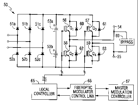
Figure 1 b shows a typical power cell or converter such as A, _5, B ~ _S and C
~ _5, as
shown in Figure 1 a. However, it is to be understood that other power cells or
power
converters can°be utilized in practicing this invention. The power cell
and control
shown in Figure 1b is similar to that shown in U.S. Patent 5,625,545. However,
the
master controller provides for control of the individual power cell in a
manner that
permits high output operation during a failed mode. Power cell 50, as shown,
is a
power converter which converts the three-phase incoming power into a DC
component
through utilization of a rectifier composed of diodes 51 a 51 ~ and 52a 52~.
The output
of this rectifier is then directed across capacitors 53a and 53b, which can
provide storage
and smoothing of the DC output. Capacitors 53a and 536 are representative of a
capacitor bank, and the precise amount of capacitance necessary depends upon
the
specific application. The DC power in the converter can be selectively appliEd
to the
converter outputs 54 and 55 using a pulse-width modulated (PWM) method. The
pulse-width modulation may be implemented using a bridge converter which is
composed of semiconductor switches such as Q1~. Any type of acceptable switch
element can be used; and depending on the power level, various solid-state
components
may be chosen. As shown, the converter output utilizes four transistors 56,
57, 58 and
59. In such a pulse-width modulated operation the switches can be considered
either
fully on or fully off as they operate. The circuit shown in Figure 1 b also
utilizes four
diodes 60-63 across each of the solid-state switch units. As will be
understood in most
CA 02272202 1999-OS-19
- 10-
applications, it is desirable that the power cells or converters utilized in a
multiconverter arrangement be similar and constructed in a form so as to limit
the
number of subassemblies and permit converters to be interchangeable within the
same
drive. Converter 50 as shown in Figure 1 b could be utilized for all of the 15
converters
in Figure 1 a. Also shown as part of the power converter in Figure 1 b is a
bypass 69.
The bypass may also be constructed as an integral part of a converter
subassembly in a
drive unit. In other applications the bypass 69 can be separately mounted. The
bypass
69 may be mechanical, electrical or solid state. As presently preferred, the
bypass unit
utilized would be solid state and similar to that shown in Figure 9 of U.S.
Patent
5,625,545. When bypass 69 is operated, it in effect creates a shunt path
between the
respective output lines 54 and 55 of the converter. As such, current can then
be earned
through the bypass 69 instead of the converter. If a failed converter which
has failed in
an open-circuit mode is not bypassed, the current through that leg gbes
tot~ero. It is
therefore desirable to have a bypass circuit such as 69 on each of the
respective
corwerter outputs. Many ways are known as to monitoring and detecting a failed
cell, ' --
and these may be used. A simple method is to compare cell output voltage to
the
commanded output. Other methods can include checking or verifying cell
components
or use of diagnostics routines. While the discussion of the invention may at
times for
simplicity imply that only a single cell fails, it is to be understood that
the invention
also covers apparatus and methods utilized to permit continued operation with
one or
more cells having failed in a given leg or legs. As such, the invention can
operate not
CA 02272202 1999-OS-19
-11-
only when a single cell such as Al in Figure la fails but would also provide
increased
effective operation should multiple cells such as, for example, A,, B2, B3 and
C4 fail.
As shown in Figure 1b, the converter is controlled through the utilization of
a
local controller, such as shown at reference 65. It may be desirable that the
local
controller also be associated with and contained in the individual cell or
converter. As
such, it will control the specific converter, such as utilization of pulse-
width modulation
or other control techniques. The operation of the converter may be utilized to
control
r_ot only the output voltage but to control it in a manner that results in
specific desired
vvaveforms. The operation of the local controller may be operated as described
in the
previously referenced patent. When the local controller is located on the
individual
converter, it may be desirable that the control signals received from the
master
controller 67 are transmitted to the local controller through utilization of a
fiber optic
system, such as for example a fiber optic control link 66. It is to be
understood that vn'
practicing the invention, certain control functions may be grouped together in
the
master control such that a local controller is not necessary, and that signal
transfer may
be utilized in other means besides the utilization of fiber optics, such as
traditional
wiring.
In instances where a local controller is contained in the individual power
cell
subassembly, signals to that assembly may be generated from a master
controller.
Figure 1 c shows a master controller 70, which is utilized to generate
different signals
VA*, VB* and V~*. These signals VA*, VB* and V~* are commands or replicas of
the
desired voltage output from the respective converters on Leg A, Leg B, and Leg
C.
CA 02272202 1999-OS-19
-12-
Master controller 70 feeds control signal VA* to the A leg converters A1
through A5,
respectively. Similarly, the master controller can control a signal, VB*, to
controllers
B ~ through B5. The master controller can also direct a signal to the third
leg, C, through
signal V~* to converter C, through C5. A PWM modulator can be used to convert
each
voltage comnrumd into variable duty-cycle switching patterns for the
transistors 56, 57,
58, and 59 in Figure 1b. It is understood that the control scheme shown in
Figure lc is
only one of many control schemes that may be utilized in practicing the
invention.
While prior practice in response to a failed cell has been to short out equal
numbers of cells in all three phases, even though some of such cells are still
functional,
the invention utilizes a method in which all functional cells can contribute
to a balanced
output voltage.
Figure 1 d shows some embodiments that alternatively may be used for bypass
of a failed. cell. Alternative i in Figure 1 d shows a power converter cell
oeing bypassed
by the contacts of a relay or contactor. When the contact, shown in its open
position is
energised by the solenoid, a shunt path is created between the cell output
terminals. An
alternative bypass may be utilized as shown in ii. In this alternative, a trip
release
device causes a spring loaded contact to provide a shunt path between the cell
output
terminals. The trip release device may be electrically or mechanically
operated, and in
some embodiments may function as an open circuit detection device. iii shows a
power
converter which has across its output terminals a bypass circuit utilizing two
silicon
controlled rectifiers having reversed polarities. By turning on both SCRs a
shunt path
exists between the cell output terminals. Depending upon the cost and specific
CA 02272202 1999-OS-19
-13-
application, a similar bypass may be constructed using series transistors as
shown in
alternative iv.
Figure 2 shows a typical array of series-connected cells drawn to illustrate
the
voltage from each leg and the phase displacement between legs. Each cell is
capable of
generating AC-output voltage of, for example, 480 volts. Each cell is
represented by a
circle, with 5 cells connected in each leg between the neutral point N and the
respective
points A, B and C. As shown, such an array can typically generate up to
approximately
2,400 volts from point N to each of points A, B and C. If the control makes
these three
voltages equal in magnitude and mutually phase displaced by 120°, then
the array will
produce a balanced three-phase AC output voltage. In this case the maximum
available
line-to-line output voltage from the array shown in Figure 2 can be 4,160
volts. If one
or more cells fail, it is possible to short-circuit the cell output terminals
and continue
operation at a reduced voltage. The inactive cell or cells can be bypassed, as
was
described in Figure 1 b.
Figure 3 shows the voltage available after cells A4 and AS have been bypassed.
Because they have been bypassed, they do not show in the voltage diagram in
Figure 3,
as they do not contribute to the total voltage in the array. Bypassed cells A4
and AS
were in leg A, which extends from N to point A. As shown in Figure 3, only
three
cells, A1, A2 and A3, now remain in the leg from N to A. This is because there
is no
component of voltage remaining from the bypass cells. As a result, the maximum
voltage available from leg A (between point N and point A) has been reduced by
40%
to approximately 1,440 volts. As shown, the full voltage is still available in
the other
CA 02272202 1999-OS-19
-14-
legs from N to C and from N to B. If the control would continue to maintain
the
mutual-phase displacement angle at 120°, for example, then the output
voltage will be
unbalanced, as the voltage VCB would be much larger than the voltages VAC and
VBA. Such an unbalanced output voltage would be unsuitable for driving a load
such
as a standard AC induction motor. To avoid this undesirable condition and
still
maintain some operation of the load, it has been a practice in prior art after
one or more
cells have failed to bypass the same number of cells in all three phases. Even
though
many of these cells are still fully functional, the desire to balance the
output voltage to
the load has exceeded the desire to use all available cells. In this condition
the
maximum output voltage from the entire array is then limited to the capacity
of the
phase having the most failed cells in a leg. The extra power capacity
available in
functional cells that have been bypassed to maintain a balanced output is not
utilized.
Figure 4 shows the array of Figure 3 after failed cells A4 and AS have been
bypassed';
and in addition, functional cells B4, B5, C4, and CS have also been bypassed.
The
~naxirnum balaclced line-to-line voltage in this figure is 60% of the rated
voltage or, in
the example, 2,494 volts. It is important to understand that the connection
from the
array of converters or cells to the motor terminals normally consists of only
three wires.
The neutral point, N, of the array is usually not connected to the neutral of
the motor.
Therefore, it does not matter to the motor whether the leg voltages from point
N to
points A, B and C have the same magnitude or even whether they are mutually
phase-
displaced by 120°. The motor requires only that the line-to-line
voltages VAC, VBA
and VCB have equal magnitude and are mutually phase-displaced by 120°.
While the
CA 02272202 1999-OS-19
-15-
circuitry of Figure 4 provides balanced-output voltages and a phase
displacement of
120°, it does not utilize the full capacity of all of the functional
cells in the drive.
Figure Sa shows how an array such as Figure 1 could be configured after
failure
of cells A4 and A5. The figure assumes that cells A4 and A5, because of
failure, have
been bypassed and therefore have no contribution from these cells to the
overall voltage
in leg A, the voltage from N to A. The operation of the drive to achieve the
voltage
diagram in Figure 5 utilizes a phase angle between phase B and C that has been
reduced
from 120° to 95°. The remaining angles between A and C and
between B and A have
been increased from 120° to 132.5°. These angles now result in
the line-to-line
voltages VAC, VBA and VCB having equal magnitudes. In addition, the mutual
phase
displacement in Figure Sa is 120° between VAC, VCB and VBA. The maximum
balanced line-to-line voltage now available as shown in Figure 5 is 85% of the
rated
volW ge, or 3,542 volts. As the motor still experiences balance of the three-
phase
vcpltages, it will continue to draw balanced three-phase currents, which have
a mutual-
phase displacement of 120°. However, since the cell voltages no longer
have a mutual-
phase displacement of 120°, the angle between the cell voltage and the
cell current may
now vary among the phases. At light loads, when the motor current lags the
motor
voltage by nearly 90°, some of the cells may experience a cell current
which lags the
cell voltage by more than 90°. This can cause the cells to absorb
energy, which they
may not be able to dissipate or regenerate. Therefore, it may be desirable to
avoid
operation in this manner under light loads. Appropriate current or load-
sensing can be
implemented when light load operation of a drive utilizing this invention is
desired.
CA 02272202 1999-OS-19
- 16-
Figure Sb shows another example, where one cell has failed on Leg B (BS) and
two have failed in Leg C (C4 and CS). Here the angle between A and B has been
reduced to 96.9° while the angle between A and C has been reduced to
113.1 °. This
again gives balanced line-to-line voltages of 3249 volts, or 78% of rated.
Figure Sc shows another examples where B4, B5, C3, C4 and CS have all been
bypassed. The adjustment still allows 51% of voltage, or 2121 volts.
The control angles required will depend on the number of functional cells
remaining in each phase. The specific values for the phase-to-phase
relationship can be
calculated in the control as a failed condition is detected. In other
instances, it may be
desirable to have predetermined phase angles that represent given failure
conditions.
Figures 3, Sa, Sb and Sc show specific failure conditions. All of these
examples utilize
five cells per phase. It is obvious that other failed conditions can exist in
the five cell
per phase structure. In addition, the invention can be practiced utilizing any
number of
cells per phase. Once the number of cells utilized per phase in a given
application is
known, such as for example, five cells per leg, the fault specifics can be
determined and
appropriate leg-to-leg phase angle can be calculated. In lieu of calculating
the specific
leg-to-leg phase angle, it may desirable to have certain fault conditions
programmed
into the system. These may be predetermined values for given fault situations.
A
lookup table or tables can be utilized in practicing the invention. Tables 1-7
which
follows give general values of the leg-to-leg phase relationship for power
supplies
utilizing anywhere from two to eight cells per leg. In these tables, the legs
are assumed
to be in a three-phase Y arrangement having legs A, B and C. The table has
been
CA 02272202 1999-OS-19
- 17-
abbreviated in that it gives the same values without regard to which cell in a
given leg
fails. In addition, since a failure condition in a power supply results in
identical phase
relationships without regard to which legs have the number of failures, a
power supply
with A=5, B=3 and C=5, is the same as a power supply having active cells A=5,
B=5
and C=3. The table, therefore, proviues an easy reduced form in which to cover
all of
these combinations. In the table, the A cell is always listed as having the
most number
of active cells, the B, second most number of active cells, and C the least
number of
active cells. Tables 1-7 could be used in a microprocessor scheme as lookup
tables to
determine the proper phase relationship in a power supply having failed cells.
In the
table, the term Vmax % is used to indicate the maximum voltage that would be
available under a failed condition as a percentage of the normal line-to-line
voltage.
All of the phase angles are in relationship to the normal A vector in a power
supply
having r:a_}ailed cells. As an example, Are is the angle between the A leg in
a failed
mode as compared to the A leg in an unfailed mode. All of the angles given are
in
relation to the v;,ctor for the A leg in an unfailed mode. Because the
examples given
previously related to five cells per leg these examples can be seen in Table
4.
TABLE 1
Original number of cells = 2
A cells=1B cells=1C =0Vmax%= 28.9Are=30.0Bo = Ca=272.3
cells 90.0
A cells=1B cells=1C =1Vmax%= 50.0Acr=0.0Ber=120.0Cry=240.0
cells
A cells=2B cells=1 C =1Vmax%= 50.0Ara=0.0Bra=60.0 Cry=300.0
cells
A cells=2B cells=2 C =0Vmax%= 57.7Ara=30.0Bra= Cep=272.3
cells 90.0
A cells=2B cells=2 C =1Vmax%= 80.9Ana=15.5Bay=104.5Ce=240.0
cells
A cells=2B cells=2 C =2Vmax%=100.0Are=0.0Bet=120.0Cry=240.0
cells
CA 02272202 1999-OS-19
-18-
TABLE 2
Original number of cells = 3
A cells=1B cells=1C =0Vmax%= Are=30.0Bra= Cra=272.3
cells 19.2 90.0
A cells=1B cells=1C =1Vmax%=33.3 Aer=0.0Bay=120.0Cra=240.0
cells
A cells=2B cells=1C =1Vmax%=33.3 Aa=0.0Bg=60.0 Cry=300.0
cells
A cells=2B cells=2C =0Vmax%=38.5 Are=30.0Ber= Ce=272.3
cells 90.0
A cells=2B cells=2C Vmax%=53.9 Are=15.5Bra=104.5Cep=240.0
cells=1
A cells=2B cells=2C =2Vmax%=66.7 Are=0.0Ber=120.0Cry=240.0
cells
A cells=3B cells=2C 2 Vmax%=75.5 Are=0.0Ber=101.4Cry=258.6
cells=
A cells=3B cells=3 C 0 Vmax%=57.7 Are=30.0Bra= Cra=272.3
cells= 90.0
A cells=3B cells=3C 1 Vmax%=73.6 Ara=20.4Bay= Cra=240.0
cells= 99.6
A cells=3B cells=3 C 2 Vmax%= Ao=10.5Bra=109.5Cra=240.0
cells= 87.8
A cells=3 B cells=3 C 3 Vmax%=100.0 Are=0.0Bra=120.0Cry=240.0
cells=
TABLE 3
Original number of cells = 4
A cells=1B cells=1 C 0 Vmax%= 14.4A~=30.0Be= Car=272.3
cells= 90.0
A ctsll~---1B cells=1 C 1 Vmax%= 25.0Ana=0.0 Bo=120.0Cer=240.0
cells=
t'1 2B cells=1 C 1 Vmax%= 25.0Ao=0.0 Bo=60.0 Cep=300.0
cells= cells=
A cells=2B cells=2 C 0 Vmax%= 28.9Are=30.0Bra= Cg =272.3
cells= 90.0
A cells=2B cells=2 C 1 Vmax%= 40.5Are=15.5Bo=104.5Cep=240.0
cells=
A cells=2B cells=2 C 2 Vmax%= 50.0Are=0.0 Bra=120.0Cry=240.0
cells=
A cells=3B cells=2 C 2 Vmax%= 56.6Are=0.0 Bra=101.4Cra=258.6
cells=
A cells=3B cells=3 C 0 Vmax%= 43.3Ara=30.0Bra= Car=272.3
cells= 90.0
A cells=3B cells=3 C 1 Vmax%= 55.2Are=20.4Bo= Cry=240.0
cells= 99.6
A cells=3B cells=3 C 2 Vmax%= 65.8Aer=10.5Ber=109.5Cg =240.0
cells=
A cells=3B cells=3 C 3 Vmax%= 75.0Aar=0.0 Ber=120.0Cry=240.0
cells=
A cells=4B cells=2 C 2 Vmax%= 50.0Are=0.0 Bg=60.0 Cg=300.0
cells=
A cells=4B cells=3 C 1 Vmax%= 52.1Are=16.1Beg= Cep=315.8
cells= 76.2
A cells=4B cells=3 C 2 Vmax%= 71.5Are=7.2 Bra=96.2 Cra=260.7
cells=
A cells=4B cells=3 C 3 Vmax%= 82.3Ara=0.0 Ber=108.2Cep=251.8
cells=
A cells=4B cells=4 C 0 Vmax%= 57.7Ao=30.0Bg= Cep=272.3
cells= 90.0
A cells=4B cells=4 C 1 Vmax%= 69.8Ao=22.8Bar= Cra=240.0
cells= 97.2
A cells=4B cells=4 C 2 Vmax%= 80.9Ara=15.5Bar=104.5Cg =240.0
cells=
A cells=4B cells=4 C 3 Vmax%= 91.0Ae~=8.0 Beg=112.0Cra=240.0
cells=
A cells=4B cells=4 C 4 Vmax%=100.0Ao=0.0 Ber=120.0Cry=240.0
cells=
CA 02272202 1999-OS-19
- 19-
TABLE 4
Original number of cells = 5
A cells=1B cells=1C =0Vmax%=11.5Aar=30.0Bra= C~=272.3
cells 90.0
A cells=1B cells=1C =1Vmax%=20.0Aa= 0.0Beg=120.0C~=240.0
cells
A cells=2B cells=1C =1Vmax%=20.0Aa~=0.0Ba=60.0 Cra=300.0
cells
A cells=2B cells=2C =0Vmax%=23.1Ae~=30.0Bra= C~=272.3
cells 90.0
A cells=2B cells=2C =1Vmax%=-32.4 Aer=15.5Bra=104.5C~=240.0
cells
A cells=2B cells=2C =2Vmax%=40.0Are=0.0Bay=120.0C~=240.0
cells
A cells=3B cells=2C =2Vmax%= Ara=0.0Bra=101.4Cry=258.6
cells 45.3
A cells=3B cells=3C =0Vmax%=34.6Aer=30.0Beg= Cep=272.3
cells 90.0
A cells=3B cells=3C =1Vmax%=44.2Aer=20.4Be = Cer=240.0
cells 99.6
A cells=3B cells=3C =2Vmax%=52.7Ara=10.5B~ =109.5Cry=240.0
cells
A cells=3B cells=3C =3Vmax%=60.0Ae~=0.0B~=120.0Cra=240.0
cells
A cells=4B cells---2 C: =2Vmax%=40.0A~= 0.0Bra=60.0 Car=300.0
cells
A cells=4 B cells=3C =1Vmax%=41.7Ag= 16.1Ber= Cep=315.8
cells 76.2
A cells=4B cells=3C =2Vmax%=57.2A~= 7.2Bra=96.2 Cer=260.7
cells
A cells=4 B cells=3C =3Vmax% 65.8Are=0.0Beg=108.2Cer=251.8
cells =
A cells=4B cells=4 C =0Vmax%=46.2A~= 30.0Bra= Cer=272.3
cells 90.0
A cells=4B cells=4C =1Vmax%=55.8Ara=22.8B~ = Cep=240.0
cells 97.2
A cells=4B cells=4C =2Vmax%=64.7A~= 15.5Bas=104.5Cep=240.0
cells
A cells=4B cells=4 C =3Vmax%=72.8Ana=8.0Bra=112.0Cra=240.0
cells
A cells=4B c~e'ls~-4 C =4Vmax%= A~= 0.0Bra=120.0Cry=240.0
cells 80.0
A cells---5B'<.veils=3 C =2Vmax%=51.0Are=6.5Beg=67.6 Cg=304.9
cells
A cells=5B cells=3C =3Vmax%=69.1Ara=0.0Bra=93.6 Cg=266.4
cells
A cells=SI3 =4C =1Vmax%= Are=18.9Bar= Car=316.1
cells cells 53.4 79.6
A cells=5B cells=4 C 2 Vmax~'=69.0Acr=11.6Bra= Ce=262.1
cells= 93.9
A cells=5B cells=4 C 3 Vmax%= Are=5.9Ber=102.8Ce=252.8
ceTis= 78.1
A cells=5B cells=4 C 4 Vmax%= A~= 0.0Ber=111.3Cry=248.7
cells= 86.1
A cells=5B cells=S C 0 Vmax%=57.7Are=30.0Bra= Cep=272.3
cells= 90.0
A cells=5B cells=S C 1 Vmax%=67.4Are=24.3Bra= Cry=240.0
cells= 95.7
A cells=5B cells=5 C 2 Vmax%= Ae~=18.5Bar=101.5Cap=240.0
cells= 76.6
A cells=5B cells=5 C 3 Vmax%= Are=12.5Bar=107.5Car=240.0
cells= 85.1
A cells=5B cells=5 C 4 Vmax%=92.9Ae~=6.4Beg=113.6C~=240.0
cells=
A cells=5B cells=S C 5 Vmax%=100.0Ara=0.0Bar=120.0Cep=240.0
cells=
CA 02272202 1999-OS-19
-20-
TABLE 5
Original number of cells = 6
A cells=1B cells=1 C 0 Vmax%= 9.6Are=30.0 B~=90.0 Cer=272.3
cells=
A cells=1B cells=1 C 1 Vmax%= 16.7Ae = Be~=120.0C~ =240.0
cells= 0.0
A cells=2B cells=1 C 1 Vmax%= Ae~= B~=60.0 Cep=300.0
cells= 16.7 0.0
A cells=2B cells=2 C 0 Vmax%= 19.2Ae = Bar= C~ =272.3
cells= 30.0 90.0
A cells=2B cells=2 C 1 Vmax%= 27.0Aer= Be=104.5C~ =240.0
cells= 15.5
A cells=2B cells=2 C 2 Vmax%= 33.3A~ = B~=120.0C~ =240.0
cells= 0.0
A cells=3B cells=2 C 2 Vmax%= 37.7Ae = Bra=101.4C~a=258.6
cells= 0.0
A cells=3B cells=3 C 0 Vmax%= Ae = B~= C~a=272.3
cells= 28.9 30.0 90.0
A cells=3B cells=3 C 1 Vmax%= Ae~= B~= C~ =240.0
cells= 36.8 20.4 99.6
A cells=3B cells=3 C 2 Vmax%= 43.9Aer= Bar=109.5C~ =240.0
cells= 10.5
A cells=3B cells=3 C 3 Vmax%= 50.0A~ = Bra=120.0Cry=240.0
cells= 0.0
A cells=4B cells=2 C 2 Vmax%= 33.3Are= B~=60.0 Cep=300.0
cells= 0.0
A cells=4B cells=3C 1 Vmax%= Air= Bs~= C~a=315.8
cells= 34.7 16.1 76.2
A cells=4 B cells=3 C 2 Vmax%= 47.7Are= B~=96.2 Cap=260.7
cells= 7.2
A cells=4 B cells=3 C 3 Vmax%= Acr= Bay=108.2Cep=251.8
cells= 54.9 0.0
A cells=4B cells=4 C 0 Vmax%= A~ = Bra= Cep=272.3
cells= 38.5 30.0 90.0
A cells=4B cells=4 C 1 Vmax%= 46.5Are= Be= C~ =240.0
cells= 22.8 97.2
A cells=4B cells=4 C 2 Vmax%= 53.9Ara= B~=104.5Car=240.0
cells= 15.5
A cells=4B cells=4 C 3 Vmax%= Ana= Ber=112.0Cap=240.0
cells= 60.7 8.0
A cells=4R :ells=4 C 4 Vmax%= 66.7A~=0.0 Bra=120.0Cra=240.0
cells=
A cells---.a B cells=3 C 2 Vmax%= 42.5Ana=6.5 Bra=67.6 Ca=304.9
cells=
A cells=5B cells=3 C 3 Vmax%= 57.6Ana=0.0 Bay=93.6 Car=266.4
cells=
A cells=5B cells=4 C 1 Vmax%= 44.5Ana=18.9 Bcr= Cap=316.1
cells= 79.6
A cells=5B cells=4 C 2 Vmax%= 57.5Are=11.6 Bra= C~ =262.1
cells= 93.9
A cells=5B cells=4 C 3 Vmax%= 65.1A~=5.9 Bra=102.8Cra=252.8
cells=
A cells=5B cells=4 C 4 Vmax%= 71.7A~=0.0 Beg=111.3Cep=248.7
cells=
A cells=5B cells=5 C 0 Vmax%= 48.1Are=30.0 Bra= Cg =272.3
cells= 90.0
A cells=5B cells=S C 1 Vmax%= 56.2Ara=24.3 Bra= Cer=240.0
cells= 95.7
A cells=5B cells=5 C 2 Vmax%= 63.8Acr=18.5 Bra=101.5C~ =240.0
cells=
A cells=5B cells=5 C 3 Vmax%= Are=12.5 Bra=107.5Cer=240.0
cells= 70.9
A cells=SB cells=5 C 4 Vmax%= 77.4Am=6.4 Ber=113.6Cg =240.0
cells=
A cells=5B cells=5 C 5 Vmax%= 83.3Ara=0.0 Bra=120.0Car=240.0
cells=
A cells=6B cells=3 C 3 Vmax%= 50.0Ae~=0.0 Ba=60.0 Ca=300.0
cells=
A cells=6B cells=4 C 3 Vmax%= Are=4.8 Bra=91.2 Cry=268.4
cells= 67.3
A cells=6B cells=4 C 4 Vmax%= 75.5A~=0.0 Ber=101.4Cry=258.6
cells=
A cells=6B cells=5 C 1 Vmax%= 55.1Are=20.5 Bay= Car=311.3
cells= 82.4
A cells=6B cells=5 C 2 Vmax%= 67.2Are=14.5 Ber= Cer=263.2
cells= 92.7
A cells=6B cells=5 C 3 Vmax%= 75.1Ara=9.8 Beg=99.8 Cep=253.6
cells=
A cells=6B cells=5 C 4 Vmax%= Ara=5.0 Bra=106.5Ca =249.3
cells= 82.1
A cells=6B cells=5 C 5 Vmax%= 88.5Aa~=0.0 Bra=113.1Ce =246.9
cells=
CA 02272202 1999-OS-19
-21 -
A cells=6B cells=6 C =0Vmax%=57.7Aa~=30.0Bay= Cry=272.3
cells 90.0
A cells=6B cells=6 C =1Vmax%=65.9Aa= 25.2Be = Ce=240.0
cells 94.8
A cells=6B cells=6 C =2Vmax%=73.6Are=20.4Bo = Cep=240.0
cells 99.6
A cells=6B cells=6 C =3Vmax%=80.9Are=15.5Bg =104.5Cer=240.0
cells
A cells=6B cells=6 C =4Vmax%= Are=10.5Bo =109.5Cry=240.0
cells 87.8
A cells=6B cells=6 C =5Vmax%=94.1Ara=5.4Bra=114.6Cep=240.0
cells
A cells=6B cells=6 C =6Vmax%=100.0 Are=0.0Beg=120.0Cra=240.0
cells
TABLE 6
Original number of cells = 7
A cells=1B cells=1C =0Vmax%= Are=30.0Bo=90.0 Cry=272.3
cells 8.2
A cells=1B cells=1C =1Vmax%= Ae = Bra=120.0Cry=240.0
cells- 14.3 0.0
A cells=2B cells=1C =1Vmax%= Aa~= Bra=60.0 Cry=300.0
cells 14.3 0.0
A cells=2B cells=2C =0Vmax%= Ae~= Bra= Cra=272.3
cells 16.5 30.0 90.0
A cells=2B cells=2C =1Vmax%= Ao = Bo =104.5Cep=240.0
cells 23.1 15.5
A cells=2B cells=2C =2Vmax%= Aa = Bo=120.0Cra=240.0
cells 28.6 0.0
A cells=3B cells=2C =2Vmax%= Aer= Bra=101.4Cry=258.6
cells 32.3 0.0
A cells=3B cells=3C =0Vmax%= Air= Bo = Cra=272.3
cells 24.7 30.0 90.0
A cells=3B cells---3C =1Vmax%= Ara=20.4Bra= Co=240.0
cells 31.5 99.6
A cells=3B cells--~~ =2Vmax%= Ara=10.5Bra=109.5Cry=240.0
3 :ells 37.6
A cells=3B cells=3C Vmax%= Ao=0.0 Beg=120.0Cep=240.0
cells=3 ~~2.9
A cells=4B cells=2C =2Vmax%= Ae=0.0 Bay=60.0 Cra=300.0
cells 28.6
A cells---4B cells=3C =1Vmax%= A~=16.1Bra= Co=315.8
cells 29.8 76.2
A cells=4B cells=3C 2 Vmax%=10:9Are=7.2 Bra=96.2 Co=260.7
cells=
A cells=4B cells=3C 3 Vmax%= Ao=0.0 Ba=108.2Co=251.8
cells= 47.0
A cells=4B cells=4C 0 Vmax%= Air=30.0Bra= Cra=272.3
cells= 33.0 90.0
A cells=4B cells=4C 1 Vmax%= Ae~=22.8Bar= Co=240.0
cells= 39.9 97.2
A cells=4B cells=4C 2 Vmax%= Are=15.5Bar=104.5Cer=240.0
cells= 46.2
A cells=4B cells=4C 3 Vmax%= Are=8.0 Be=112.0Ce=240.0
cells= 52.0
A cells=4B cells=4C 4 Vmax%= Are=0.0 Bra=120.0Cra=240.0
cells= 57.1
A cells=5B cells=3C 2 Vmax%= Ao=6.5 Bra=67.6 Ccr=304.9
cells= 36.4
A cells=5B cells=3C 3 Vmax%= Are=0.0 Be=93.6 Cry=266.4
cells= 49.4
A cells=5B cells=4C 1 Vmax%= Ara=18.9Bra= Cry=316.1
cells= 38.2 79.6
A cells=5B cells=4C 2 Vmax%= Ara=11.6Bra= Co=262.1
cells= 49.3 93.9
A cells=5B cells=4C 3 Vmax%= Ara=5.9 Beg=102.8Cra=252.8
cells= 55.8
A cells=5B cells=4C 4 Vmax%= Are=0.0 Bar=111.3Cry=248.7
cells= 61.5
A cells=5B cells=5C 0 Vmax%= Are=30.0Bra= Co=272.3
cells= 41.2 90.0
A cells=5B cells=5C 1 Vmax%= Are=24.3Bar= Cra=240.0
cells= 48.2 95.7
A cells=5B cells=5C 2 Vmax%= Are=18.5Bra=101.5Cep=240.0
cells= 54.7
A cells=5B cells=5C 3 Vmax%= Are=12.5Bra=107.5Cep=240.0
cells= 60.8
CA 02272202 1999-OS-19
-22-
A =5B cells=5C cells=4Vmax%=66.3Aa= 6.4Bra=113.6Ce=240.0
cells
A =5B cells=5C cells=5Vmax%=71.4Aa~=0.0Bay=120.0Cra=240.0
cells
A =6B cells=3C cells=3Vmax%=42.9Aa~=0.0Bra=60.0Cra=300.0
cells
A =6B cells=4C cells=3Vmax%=57.7Are=4.8Bra=91.2Cry=268.4
cells
A =6B cells=4C cells=4Vmax%=64.7Are=0.0Be=101.4Cep=258.6
cells
A =6B cells=5C cells=1Vmax%=47.2Are=20.5Bra= Cep=311.3
cells 82.4
A =6B cells=5C cells=2Vmax%=57.6Ag= 14.5Bra= Cep=263.2
cells 92.7
A =6B cells=5C cells=3Vmax%= Ae= 9.8Bg=99.8Cs~=253.6
cells 64.4
A =6B cells=5C cells=4Vmax%--- A~= 5.0Bra=106.5Cra=249.3
cells 70.4
A =6B cells=5C cells=5Vmax%=75.9Aer=0.0Bra=113.1Cg=246.9
cells
A =6B cells=6C cells=0Vmax%=49.5Ara=30.0Bra= Cry=272.3
cells 90.0
A =6B cells=6C cells=1Vmax%=56.5Ae~=25.2Bg = C~=240.0
cells 94.8
A =6B cells=6C cells=2Vmax%=63.1Ara=20.4Bra= Cry=240.0
cells 99.6
A =6B cells=6C cells=3Vmax%=69.3Ara=15.5Bra=104.5Cer=240.0
cells
A =6B cells=6C cells=4Vmax%= Ae~=10.5Bay=109.5Cer=240.0
cells 75.2
A =6B cells=6C ;,ells=5Vmax%=80.7Are=5.4Bra=114.6Car=240.0
cells
A 6 B cells=ti G cells=6Vmax%= Air=0.0B~=120.0Car=240.0
cells= 85.7
A 7 B cells=4 C cells=3Vmax%= Ara=4.6Bra=68.0Cra=299.9
cells= 52.2
A 7 B cells=4 C cells=4Vmax%--- Are=0.0Bra=89.0C~=271.0
cells= 66.0
A 7 B cells=5C cells=3Vmax% 66.0Ae= 8.2Bra=90.0C~=270.0
cells= =
A 7 B cells=5C cells=4Vmax%= Are=4.1Bra=98.2C~=259.7
cells= 73.3
A 7 B cells=5C cells=5Vmax%= Are=0.0Bra=105.6Cry=254.4
cells= 79.5
A 7 B cells=6C cells=1Vmax%=54.8Are=22.1Bra= Cry=317.0
cells= 83.0
A 7 B c~:l'.s=6C cells=2Vmax%=65.9Ara=16.6B~ = Cep=264.0
cells= 92.0
A 7 B yells=6C cells=3Vmax%=72.8Are=12.6Bra= Cep=254.2
cells= 97.8
A 7 B cells=6C cells=4Vmax%=79.1Are=8.6Be.=103.3C~=249.8
cells=
A 7 ~; =6C cells=5Vmax%=84.9Are=4.4Bra=108.8Cra=247.3
cells= cells
A 7 B cells=6C cells=6Vmax~/=90.2Are=0.0B~=114.3Cra=245.7
cells=
A 7 B cells=7C cells=0Vmax%=57.7Are=30.0Bra= Cry=272.3
cells= 90.0
A 7 B cells=7C cells=1Vmax%= Are=25.9Bra= Cry=240.0
cells= 64.7 94.1
A 7 B cells=7C cells=2Vmax%=71.4Are=21.8Bar= Cry=240.0
cells= 98.2
A 7 B cells=7C cells=3Vmax%=77.8Ara=17.6Bra=102.4Ce =240.0
cells=
A 7 B cells=7C cells=4Vmax%= Ag= 13.4Be =106.6Cep=240.0
cells= 83.9
A 7 B cells=7C cells=5Vmax%=89.6Are=9.1Beg=110.9Cra=240.0
cells=
A 7 B cells=7C cells=6Vmax%=95.0Are=4.6Bra=115.4Cry=240.0
cells=
A 7 B cells=7C cells=7Vmax%=100.0Are = Beg=120.0Cra=240.0
cells= 0.0
CA 02272202 1999-OS-19
- 23 -
TABLE 7
Original number of cells = 8
A =1B 1 C 0 Vmax%= 7.2 Are=30.0Bra=90.0 Cer=272.3
cells cells= cells=
A =1B 1 C 1 Vmax%= 12.5A~=0.0 Bra=120.0Cs~=240.0
cells cells= cells=
A =2B 1 C 1 Vmax%= 12.5Ara=0.0 Bra=60.0 Cm=300.0
cells cells= cells=
A =2B 2 C 0 Vmax%= 14.4Ara=30.0Be= Cra=272.3
cells cells= cells= 90.0
A =2B 2 C 1 Vmax%= 20.2A~=15.5Bar=104.5C~ =240.0
cells cells= cells=
A 2 B 2 C 2 Vmax%= 25.0Are=0.0 Be=120.0Cry=240.0
cells= cells= cells=
A 3 B 2 C 2 Vmax%= 28.3A~=0.0 B~=101.4Cry=258.6
cells= cells= cells=
A 3 B 3 C 0 Vmax%= 21.7Are=30.0Bra= Cry=272.3
cells= cells= cells= 90.0
A 3 B 3 C 1 Vmax%= 27.6Ara=20.4B~= Cry=240.0
cells= cells= cells= 99.6
A 3 B 3 C 2 Vmax%= 32.9Aer=10.5Bra=109.5Cry=240.0
cells= cells= cells=
A 3 B 3 C Vmax%= 37.5Are=0.0 B~=120.0Cry=240.0
cells= cells= cells=3
A 4 B 2 C 2 Vmax%= 25.0Are=0.0 Bra=60.0 Cra=300.0
cells= cells= cells
=
A 4 B 3 C 1 Vmax%= 26.1Ara=16.1Bra= Cer=315.8
cells= cells= cells= 76.2
A 4 B 3 C 2 Vmax%= 35.8Ag=7.2 Bar=96.2 Cry=260.7
cells= cells= cells=
A 4 B 3 C 3 Vmax%= 41.1Are=0.0 Bra=108.2Cer=251.8
cells= cells= cells=
A 4 B 4 C 0 Vmax%= 28.9Are=30.0B~t= Cg =272.3
cells= cells= cells= 90.0
A B 4 C 1 Vmax%= 34.9Aa~=22.8Bra= Cra=240.0
cells=4 cells= cells= 97.2
A 4 B 4 C 2 Vmax%= 40.5Are=15.5Bar=104.5Cg =240.0
cells= cells= cells=
A 4 B 4 C 3 Vmax%= 45.5Ara=8.0 Bra=112.0Cry=240.0
cells= cells= cells=
A 4 B 4 C 4 Vmax%= 50.0Ara=0.0 Bra=120.0Cra=240.0
cells= cells= coils=
A 5 B ~cells-=2 Vmax%= 31.9Ara=6.5 Bg=67.6 Cra=304.9
cells= cells=3
A 5 B 3 C 3 Vmax%= 43.2Ae=0.0 Bg=93.6 C~=266.4
cells= cells= cells=
A 5 B 4 C 1 Vmax%= 33.4Ae=18.9Bg= Ce =316.1
cells= cells= cells= 79.6
A 5 B 4 C 2 Vmax%= 43.?Are=11.6Bar= Cra=262.1
cells= cells= cells= 93.9
A 5 B 4 C 3 Vmax%= 48.8A~=5.9 Be=102.8Cra=252.8
cells= cells= cells=
A 5 B 4 C 4 Vmax%= 53.8Ae=0.0 Bra=111.3Cra=248.7
cells= cells= celis=
A 5 B 5 C 0 Vmax%= 36.1A~=30.0Bar= Cra=272.3
cells= cells= cells= 90.0
A 5 B 5 C 1 Vmax%= 42.2A~=24.3Bra= Cra=240.0
cells= cells= cells= 95.7
A 5 B 5 C 2 Vmax%= 47.9Ara=18.5Bg=101.5Cry=240.0
cells= cells= cells=
A 5 B 5 C 3 Vmax%= 53.2Are=12.5Beg=107.5Cra=240.0
cells= cells= cells=
A 5 B 5 C 4 Vmax%= 58.0Are=6.4 Beg=113.6Cry=240.0
cells= cells= cells=
A S B 5 C 5 Vmax%= 62.5A~=0.0 Bra=120.0C~ =240.0
cells= cells= cells=
A 6 B 3 C 3 Vmax%= 37.5Are=0.0 Bra=60.0 Cap=300.0
cells= cells= cells=
A 6 B 4 C 3 Vmax%= 50.5Ara=4.8 Bra=91.2 Cep=268.4
cells= cells= cells=
A 6 B 4 C 4 Vmax%= 56.6Ae=0.0 Bra=101.4Cry=258.6
cells= cells= cells=
A 6 B 5 C 1 Vmax%= 41.3Are=20.5Bra= Cry=311.3
cells= cells= cells= 82.4
A 6 B 5 C 2 Vmax%= 50.4Ara=14.5Bra= Cry=263.2
cells= cells= cells= 92.7
A 6 B 5 C 3 Vmax%= 56.3Ara=9.8 Bra=99.8 Ce=253.6
cells= cells= cells=
A 6 B 5 C 4 Vmax%= 61.6Ara=5.0 B~=106.5Cry=249.3
cells= cells= cells=
A 6 B 5 C 5 Vmax%= 66.4Ara=0.0 Bra=113.1Cry=246.9
cells= cells= cells=
CA 02272202 1999-OS-19
-24-
A cells=6B cells=6C cells=0Vmax%=43.3Ara=30.0Bra= Cep=272.3
90.0
A cells=6B cells=6C cells=1Vmax%=49.4Ara=25.2Be = Cra=240.0
94.8
A cells=6B cells=6C cells=2Vmax%= Ara=20.4Bra= Cra=240.0
55.2 99.6
A cells=6B cells=6C cells=3Vmax%=60.7A~= 15.5Bra=104.5C~=240.0
A cells=6B cells=6C cells=4Vmax%=65.8Ara=10.5Bra=109.5Cra=240.0
A cells=6B cells=6C cells=5Vmax%=70.6Ara=5.4Bra=114.6Cra=240.0
A cells=6B cells=6C cells=6Vmax%=75.0Ara=0.0Bra=120.0Cra=240.0
A cells=7B cells=4C cells=3Vmax%=45.6Ara=4.6Bra=68.0 Cra=299.9
A cells=7B cells=4C cells=4Vmax%=57.7Ara=0.0Bra=89.0 Cra=271.0
A cells=7B cells=5C cells=3Vmax%=57.7Ara=8.2Bra=90.0 Cra=270.0
A cells=7B cells=5C cells=4Vmax%=64.1Aer=4.1Bra=98.2 Cep=259.7
A cells=7B cells=5C cells=5Vmax%=69.5Ag= 0.0B~=105.6Cep=254.4
A cells=7B cells=6C cells=1Vmax%=47.9Ara=22.1Bra= Cra=317.0
83.0
A cells=7B cells=6C cells=2Vmax%= Ara=16.6Be = Cra=264.0
57.6 92.0
A cells=7B cells=6C cells=3Vmax%=63.7Ara=12.6Bra= Cra=254.2
97.8
A cells=7B cells=6C cells=4Vmax%= .bra=8.6Bra=103.3Cra=249.8
69.2
A cells=7B cells=6C cells=5Vmax%= Ara=4.4Bra=108.8Ca=247.3
74.3
A cells=7B cells=6C cells=6Vmax%=78.9Ara=0.0Bra=114.3Cap=245.7
A cells=7B cells=7C cells=0Vmax%=50.5Ara=30.0Bra= Cra=272.3
90.0
A cells=7B cells=7C cells=1Vmax%=56.6Ara=25.9Bra= Cra=240.0
94.1
A cells=7B cells=7C cells=2Vmax%=62.5Ara=21.8Bra= Cra=240.0
98.2
A cells=7B cells=7C cells=3Vmax%=68.1Ara=17.6B~ =102.4Cra=240.0
A cells=7B cells=7C cells=4Vmax%=73.4Ara=13.4Bra=106.6Cra=240.0
A cells=7B cells=7C cells=5Vmax/.~=~ Ara=9.1Ba=110.9Ce=240.0
78.4
A cells=7B cells=7C cells=6Vmax'/o=83.1Ae~=4.6Bra--115.4Cra=240.0
A cells=7B cells=7C cells=7Vmax%=87.5Apt=0.0Bra=120.0Cra=240.0
A cells=8B cells=4C cells=4Vmax%= Ara=0.0Be=60.0 Cra=300.0
50.0
A cells=8B cells=5C cells=3Vmax%=50.7Ara=8.2Bra=.68.4Cra=307.8
A cells=8B cells=5C cells=4 Vmax%=64.9A~= 3.6Bra=87:7 Cra=272.8
A cells=8B cells=6C cells=2 Vmax%= Ae= 16.1Bra= Cra=315.8
52.1 76.2
A cells=8B cells=6C cells=3 Vmax%= Ara=10.8Be = Cra=271.2
64.9 89.4
A cells=8B cells=6C cells=4 Vmax%= Ara=7.2Bra=96.2 Cra=260.7
71.5
A cells=8B cells=6C cells=5 Vmax%=77.2Ara=3.7B~=102.3Cra=255.2
A cells=8B cells=6C cells=6 Vmax%=82.3Ae= 0.0Bra=108.2Cra=251.8
A cells=8B cells=7C cells=1 Vmax%=55.4Ara=23.1Bra= Cra=315.3
84.2
A cells=8B cells=7C cells=2 Vmax%= Ara=18.2Bra= Cra=264.7
64.9 91.5
A cells=8B cells=7C cells=3 Vmax%=71.1Ae~=14.7Bra= Cra=254.7
96.5
A cells=8B cells=7C cells=4 Vmax%= Ara=11.2Bra=101.2Cra=250.2
76.7
A cells=8B cells=7C cells=5 Vmax%=82.0Ara=7.6Bra=105.8Cap=247.6
A cells=8B cells=7C cells=6 Vmax%=86.9A~= 3.9Bra=110.4Cra=246.0
A cells=8B cells=7C cells=7 Vmax%=91.5Ara=0.0Bra=115.2Cra=244.9
A cells=8B cells=8C cells=0 Vmax%=57.7Ara=30.0Bra= Cra=272.3
90.0
A cells=8B cells=8C cells=2 Vmax%= Ara=22.8Bra= Cra=240.0
69.8 97.2
A cells=8B cells=8C cells=3 Vmax%=75.5Ara=19.2B~ =100.8Cra=240.0
CA 02272202 1999-OS-19
-25-
A =8B cells=8C =4Vmax%=80.9 Are=15.5Bo =104.5Cra=240.0
cells cells
A =8B cells=8C =5Vmax%=86.1 Ao=11.8Bo =108.2Co =240.0
cells cells
A =8B cells=8C =6Vmax%=91.0 Ara=8.0Bra=112.0Ce=240.0
cells cells
A =8B cells=8C =7Vmax%=95.7 Ae=4.1Bra=115.9Co=240.0
cells cells
A =8B cells=8C =8Vmax%=100.0Aa~=0.0Bra=120.0Cap=240.0
cells cells
The angles given in Tables 1-7 give the optimum results, but the angles may be
fairly difficult to calculate, especially when the number of functional cells
is different in
all three phases. However, utilizing other teachings of this invention, it is
not necessary
to calculate these angles. An existing control structure can be modified to
implement a
balanced bypass control, with results almost as good as Tables 1-7. Output
voltage of
the individual cells in each leg is controlled by pulse-width modulation. This
modulation is implemented as shown in Figure 1 c by comparing command
waveforms
for each phase or leg to a group of triangular carrier waveforms. The carrier
waveforms
oscillate at the desired switching frequency for the c:;lis. 'These carrier
waveforms have
various phase angles to obtain harmonic cancellation between the cells. The
command
waveforms are simply replicas of the desired output voltages from point N to
points A,
B and C, namely the individual legs A, B and C. When the array of cells is
used to
drive a load such as a motor, the desired line-to-line output voltages are
typically
sinusoidal in nature. However, if sinusoidal command waveforms are employed,
then
the maximum available output voltage will be limited to the value where the
sine wave
amplitude becomes equal to the carrier amplitude. With three-phase sine waves,
at the
moment when one phase reaches maximum voltage, the other two phases are only
at
half of the maximum voltage with opposite polarity. This results in unused
capacity.
CA 02272202 1999-OS-19
-26-
To improve the maximum voltage limit, a control method such as shown in Figure
6 is
often used. The original sinusoidal commands, VA*, VB*, VC*, are processed as
shown in the block diagram of Figure 6. Output of this process is then sent to
the
pulse-width modulator.
Shown in Figure 6 (prior art), a block labeled SELECT MAXIMUM produces a
signal equal to the most positive of the three voltage commands at any
instant. A
similar block labeled SELECT MINIMUM produces a signal equal to the most
negative of the three voltage commands at any instant. These two signals are
added,
and the sum is divided in half. The resulting signal is hen subtracted from
each of the
original voltage commands, to produce a new set of voltage commands which are
then
sent to the pulse-width modulator. Modified voltage commands EA*, EB* and EC*
are
peak-reduced commands that are sent to the PWM control. For example, if the
magnitude of the most positive voltage comlYxand is equal to the most
negative, the
output of the sum will be zero. However, if the magnitude of the most positive
voltage
command is greater than the most negative, the output of the sum will be
positive.
When half of this difference is subtracted from all three commands, the
resulting new
command set, EA*, EB*, EC*, will have most positive and most negative values
of
equal size. As shown in Figure 6, the peak voltage reduction method subtracts
the same
signal from all three commands. Such a signal is called a "common mode
signal." The
polarity of the subtraction is always such that the command with the largest
magnitude
is reduced, while the magnitude of the one or both of the other commands is
increased.
In effect, the phases which have extra capacity are used to "help" the phase
with the
CA 02272202 1999-OS-19
-27-
greatest burden. This methodology increases the available line-to-line voltage
by 20%
over the sinusoidal case. It can also be used with the failed cell bypass
invention, with
a simple modification.
The peak voltage reduction method of Figure 6 can be modified to also
implement the new bypass invention methodology. Figure 7 shows a very simple
modification. The only change needed to the Figure 6 diagram is to introduce
adjustable gains KA, KB and KC to the sinusoidal input commands VA*, VB* and
VC*. These new gains are normally unity if no cells are bypassed. In that way
they
have no effect on the output values EA*, EB* and EC*. However, if one or more
cells
are bypassed, then the values of these gains for any phase, where the number
of
functional cells has been reduced, is increased to the ratio of the normal
cell count
divided by the actual unfailed cell count. The result is to tend to increase
the command
to the remaining cells by the amount needed to mai-nta'in-the original output
voltage.
Gain function blocks KA, KB and KC provide this function. Since this new
command
is larger than the commands to the other phases, which have lost fewer or no
cells, a
common-mode signal is generated which then reduces the burden on the remaining
cells and causes the cells in the other phase to "help" supply voltage to the
phase or
phases having legs with failed cells.
Figures 8, 9, and 10 show waveforms from Figure 7 with zero, two, and four
cells bypassed, respectively. Shown in Figure 8, the gains for the respective
legs KA,
KB, and KC, are equal to one, as no cells have failed. In Figure 7 the signals
marked
VA*, VB*, and VC* are the balanced sinusoidal voltage commands originating in
CA 02272202 1999-OS-19
-28-
other parts of the control. These signals are multiplied by gains KA, KB, and
KC
respectively to generate signals UA*, UB*, and UC*. Figure 8 shows the case of
no
cells bypassed as in Figure 2 (so that KA = 1, KB = 1, and KC = 1); therefore
in Figure
8a UA*, UB*, and UC* are also balanced sinusoidal voltages. Note that at the
instant
when UB* reaches its peak positive value, both UA* and UC* are negative, but
with
only half the magnitude of UB*. Figure 8b shows the signal UMAX from the
SELECT
MAXIMUM block, and also the signal UMIN from the SELECT MINIMUM block. In
Figure 8b only UB* has been shown for clarity; both UA* and UC* have been
omitted.
It is clear that the UMAX signal follows whichever of the signals UA*, UB* or
UC* is
the most positive, while the UMIN signal follows whichever of the signals UA*,
UB*
or UC* is the most negative. Figure 8c is the same as 8b, with the signal UCOM
added. UCOM is the result of adding together UMAX and UMIN, and dividing by
two. UCOM is the common-mode signal that wil>~e subtracted from the three
signals
UA*, UB*, and UC*. Figure 8d shows the result of that subtraction, where EA* _
UA* - UCOM, EB* = UB* - UCOM, and EC* = UC* - UCONI. Note-that these three
signals have lower peak values than UB* (or UA* or UC*, which are not shown).
At
the instant when UB* reaches its peak positive value, EB* has a smaller
positive value;
and both EA* and EC* are negative with the same magnitude as EB*. When EA*,
EB*, and EC* are used to control the PWM modulation of the cells; the effect
at that
instant will be to reduce the peak voltage magnitude required from the B-phase
cells by
increasing the magnitude required from the A-phase and C-phase cells.
CA 02272202 1999-OS-19
-29-
However, in Figure 9 cells B4 and BS have been bypassed. The waveforms in
Figure 9 correspond to the outputs from Figure 7 with cells B4 and BS
bypassed.
Figure 9 shows the same signals as Figure 8 for the case of two cells bypassed
in phase
B (as in Figure 3). The signals VA*, VB*, and VC* are still balanced, but the
gain KB
has been increased to equal the ratio of the normal cell count divided by the
remaining
un-bypassed cell count, which is 5/3 = 1.67. The other gains are unaffected,
so that KA
= 1, KB = 1.67, and KC = 1. Therefore in Figure 9a UA* and UC* are balanced
sinusoidal voltages but UB* is much larger. Figure 9b shows the signal UMAX
from
the SELECT MAXIMUM block, and also the signal UMIN from the SELECT
MINIMUM block under these conditions (UA* and UC* have been omitted for
clarity).
Figure 9c is the same as 9b, with the signal UCOM added. UCOM now contains a
significant component of the UB* signal, due to the unbalance. Figure 9d shows
the
result of subtracting UCOM from UA*, UB* and UC* to ger~EA*; EB* and EC*. Note
that these three signals have peak values lower than UB*, and that they all
have the
-- same peak values at different moments within each cycle. At the instant
when LJB*
reaches its peak positive value, EB* has a significantly smaller positive
value; and both
EA* and EC* are negative with the same magnitude as EB*. When EA*, EB*, and
EC* are used to control the PWM modulation of the cells; the effect is that
all the
remaining cells will be required to produce the same peak voltage, even though
phase
B is missing two out of five cells. If the drive output voltage is gradually
increased, all
13 remaining cells will reach their voltage limit simultaneously. This will
occur at
about 85% of the voltage available when all 15 cells were functioning.
However, if
CA 02272202 1999-OS-19
-30-
two cells had been bypassed in each phase (as shown in Figure 4), the maximum
available voltage would be only 60%.
The voltage diagram of the power circuit for such a bypass arrangement is
shown in Figure S. Hence, in this example, two cells have been bypassed in leg
B, the
constant kA has been increased from the previous value of 1 to the current
value of 1.67.
This value may be calculated from the following equation:
the total number of cells in leg X
kX = the number of nonbypassed cells in leg X
The total number of the cells in the leg includes those that are bypassed and
those that are not bypassed. As shown in the example, kA = 5/3 or 1.67.
Figure 10 shows the waveforms from Figure 7, having command outputs to the
pulse-
width modulation control, EA*, EB* and EC*. In this example cells A2, A3, A4
and AS
have been bypassed. Figure 10 shows the same signals as Figure 8 for the case
of four
cells bypassed in phase A. The signals VA*, VB*, and VC* are still balanced,
but the
gain KB has been increased to equal the ratio of the normal cell count divided
by the
remaining un-bypassed cell count, which is 5/1 = 5. The other gains are
unaffected, so
that KA = 5, KB = l, and KC = 1. Therefore in Figure 10a UB* and UC* are
balanced
sinusoidal voltages but UA* is much larger. Figure l Ob shows the signal UMAX
from
the SELECT MAXIMUM block, and also the signal UMIN from the SELECT
MINIMUM block under these conditions (UB* and UC* have been omitted for
clarity).
Figure l Oc is the same as l Ob, with the signal UCOM added. UCOM now contains
a
dominant component of the UA* signal, due to the unbalance. Figure l Od shows
the
result of subtracting UCOM from UA*, UB* and UC* to get EA*, EB* and EC*. Note
CA 02272202 1999-OS-19
-31 -
that these three signals have peak values lower than UAB*, and that they all
have the
same peak values at different moments within each cycle. At the instant when
UA*
reaches its peak positive value, EA* has a significantly smaller positive
value; and both
EB* and EC* are negative with the same magnitude as EA*. When EA*, EB*, and
EC* are used to control the PWM modulation of the cells; the effect is that
all the
remaining cells will be required to produce the same peak voltage, even though
phase A
is missing four out of five cells. If the drive output voltage is gradually
increased, all
11 remaining cells will reach their voltage limit simultaneously. This will
occur at
about 67% of the voltage available when all 15 cells were functioning.
However, if
four cells had been bypassed in each, the maximum available voltage would be
only
20%.
This results in new gain constants to the input of Figure 7. These new
constants
are KA = 5, KB = 1 and KC = 1. As previously discussed, since there are no
failures in
leg B or leg C, the constant is unity. This is derived by the total slumber of
cells in each
leg divided by the number of cells which are operational and have not been
bypassed.
In each instance with regard to legs B and C, the values are 5/5. However,
because leg
A has cells A2, A3, A4 and AS bypassed, the value for kA is equal to 5; the
total
number of cells in the leg, divided by the number of cells that are
operational, namely
1. The result is the constant kA = S. Revising these values of kA, kB and kC,
the
circuit of Figure 1 a can be operated with four power cells failed in a single
leg and still
maintain balanced output voltage to motor terminals A, B and C. Seventy-three
percent
of the operational power cells or convesrters, namely A~, B1_5 and C,_5 are
providing
CA 02272202 1999-OS-19
-32-
power to the motor. In such an operation if the practice of shunting or
bypassing an
equal number of functional cells was utilized, the maximum output voltage
would be
20% between motor terminals. However, utilizing the present invention, the
output
voltage between the terminals of the motor in a system having four failed
cells in a
single leg is equal to 67%.
Figure 11 shows a circuit diagram which can be used to provide the modified
pulse-width modulation signals EA*, EB* and EC*. Inputs VA", VB" and V~" are
fed
through gain controls 81-83, which represent the cell failure constants kA, kB
and kC.
The select minimum-select maximum circuitry utilizes a diode bridge, having
diodes 84, 86 and 88 feeding the select maximum. Similarly, diodes 85, 87 and
89
provide voltage feeds for the select minimum function. Voltage divider
circuits
utilizing resistors 94 and 95 provide the division-by-two function. The
voltage divided-
by-two function is then fed to summers 90, 91 and 92, along with the
respective gain
modified control signal values.
The method of Figures 7 or 11 almost achieves the same outputwoltages as
using calculated angles from Tables 1-7, but it does introduce small amounts
of
distortion which will often be acceptable. Since the method of Figure 7 is
simple, with
no feedback loops, it may be preferred in some cases.
Figure 12 shows a block diagram of another control function to reduce the peak
voltage command, and also to implement the new strategy, which is more complex
than
Figure 7 but gives better results. This method requires an internal feedback
loop with
CA 02272202 1999-OS-19
- 33 -
integration, but it avoids the distortion of Figure 7 and comes even closer to
achieving
the same output voltages as using the calculated angles of Table 7.
The principle difference between Figure 7 and Figure 12 is that the common-
mode signal UCOM is subtracted from the sinusoidal commands VA*, VB* and VC*
before the auljustable gains KA, KB, and KC are applied. The subtraction
occurs in the
summation functions 201, 202, and 203, while the gains are applied in blocks
204, 205,
and 206. As in Figure 7, block 207 SELECT MAXIMUM produces a signal UMAX
equal to the most positive input signal, but these input signals are now the
outputs UA*,
UB* and UC*. Similarly, block 208 SELECT MINIMUM produces a signal UMIN
equal to the most negative input signal, but these input signals are again the
outputs
UA*, UB*, and UC*.
The signals UMAX and UMIN are added in summation function 209, and
divided in half in block 210. In block 210 the signal is also divided by
Kinax, which is
equal to the largest of the three gains KA, KB, or KC. Division by Kmax is
needed for
stability in digital implementations with sampling, but is not needed in
analog
implementations. The output of block 210 is integrated with respect to time in
function
211 to produce signal UCOM.
During operation of the method of Figure 12, suppose that the most positive
signal UMAX exceeds the amplitude of the most negative signal UMIN; so that a
small
positive remnant emerges from block 209 to drive the integrator 211 via gain
block
210. This will cause the integrator output UCOM to become more positive over
time.
When this more positive signal UCOM is subtracted from VA*, VB*, and VC* in
201,
CA 02272202 1999-OS-19
-34-
202, and 203, it will cause signals UA*, UB*, and UC* to become more negative.
This
process will continue until UMAX and UMIN are equal but opposite, so that the
summation output 209 becomes zero. At this point the most positive and most
negative
signals are equal but opposite, as desired.
The method of Figure 12 is slightly superior to Figure 7 because it does not
introduce distortion and allows slightly higher output voltage. However, it is
more
complex due to the feedback path with integration. Feedback is necessary
because the
common-mode signal UCOM is derived downstream of the point where it is used.
Therefore in many cases the method of Figure 7 will be preferred.
While many of the various embodiments discussed hereinto before have utilized
bypass functions such as described in Figure 1 D, it is understood that other
arrangements may be utilized to transfer the outputs from various operating
cells.
Figure 13 shows one such transfer switch. In this diagrammatic representation
a normal
input at 301 can be connected to the output 304 via switch arm 303. ' In the
alternative
position, 303 can connect the output 304 to an alternate input 302. This SPDT
' ~-
switching arrangement is well-known to those in the electrical arts. As shown
the
switch arm 33 is driven by a fluid-operated piston 35 which can be supplied
through a
tube 36. In the preferred embodiments the fluid would be air and the tube 306
could be
of a plastic, non-electrical conducting material. Such materials are readily
available.
308 shows a source of pressurized air. This could be a captive reservoir or a
compressor or other source of pressurized fluid. Electrical operation of
solenoid
valve 307 causes switch arm 303 to move. In this arrangement a transfer switch
is used
CA 02272202 1999-OS-19
-35-
in lieu of the bypass contactors shown in Figure 1 d. One of the advantages of
such an
arrangement is that the mechanical contactor can be mounted adjacent to the
high
voltage connection areas and electrical isolation is maintained by the non-
conducting
tube 306. As a result, all high voltage would be maintained in the high
voltage area.
Electrically opela~sd solenoid valve 307 could be a two-position valve in
which fluid
from 308 is communicated to piston 305 in one position and fluid from
operating
piston 305 is exhausted to atmosphere and source 308 is cut off in the
alternative
position.
The use of a single-pole double-throw transfer switch provides for continuity
in
drives having a cell failure. In addition use of the single-pole double-throw
transfer
switch allows for the elimination of the bypass fuse needed in the single-
throw bypass
scheme. That fuse is needed for the possibility that the cell bypass must be
activated
even if the main IGBTs fail to block voltage from the bus. In the SPDT
embodih2erit,
the "break before make" actuation eliminates the possibility of bypassing a
faulted -
bridge and thus prevents the formation of a conductive plasma which might be
the
result of a total energy discharge into fuses or faulted IGBTs from the
faulted cell. This
condition might cause additional power circuit failures.
Figure 14 shows a transfer switch using a spring-loaded contact. In this case
a
pneumatic trip release device 311 is attached to a barricade 312. A non-
conducting trip
lever 313 connects the trip release mechanism to the release lever 318. The
switch
arm 318 operates in the single-pole double-throw mode between alternative
normal
output sources 316 and 317. Spring 315 biases the control arm into one of two
CA 02272202 1999-OS-19
-36-
positions. In the embodiment shown the spring 315 is pulling downward on the
switch
arm 318. However, the downward movement of switch arm 318 is limited by the
trip
lever 314. In this position 318 is in electrical conduction with the normal
source at 316.
The trip release device may be a pneumatic device powered similar to that
shown in
and discussed at Figure 13. When the trip release device is activated the
latching
mechanism of 318 and 314 disengage. As a result the switch arm 318 is moved to
be in
electrical conduction with the alternate source 317. On the device shown which
utilizes
a trip release device mounted adjacent to the barrier panel 312, it is also
conteml~lated
that the trip release device 311 could be mounted in close proximity to the
high voltage
transfer switch mechanism. In such case then it would be desirable to use the
plastic
tubing and remotely operated electrically activated solenoid valve of Figure
13 for
control of the transfer switch. Also shown in Figure 14 is an auxiliary
contact 310.
The auxiliary contact is optional and may be utilized to electrically
determine whether
the transfer switch has been operated. The transfer switch of Figure 14 is
released by
the electrical drive equipment by giving an electrical signal which either
directly or' w w'
through a pneumatic link causes the trip release device 311 to operate. 311
may, for
example, be a fluid operated piston. Once the device has operated to move from
its
normal source to its alternate source, the transfer switch will remain in that
position
until switch arm 318 is mechanically moved backward causing the latch and
lever 314,
318 to reengage. Under normal conditions both the transfer and the reset
operations
would occur under zero current conditions. The transfer switch of Figure 14
has been
shown as being a spring operated release device, such a transfer switch could
also be
CA 02272202 1999-OS-19
-37-
mechanically or pneumatically operated to go between either pole of the SPDT
switch
unit.
Figure 15 shows three cells A1, A2, and A3 operating in their normal mode in
series. Their normal input 324 would, for example, be the node of a WYE
configuration. In operation, should any one of the cells A1, A2, or A3 fail,
the
appropriate transfer switch 321, 322, or 323 operates to first disconnect that
power cell
from the circuit. As the respective switch arm of the transfer switches 321,
322 and 323
move to the other position, a series arrangement of the remaining operative
cells is
created.
While certain applications of the invention have been shown which utilize the
peak voltage reduction methodology, it is to be understood that other
embodiments may
utilize the invention to balance the output voltage between phases without
utilizing the
"peak-voltage reduction method", such as by using angles from Tables i-7. In
additiorf,
while some of the circuitry has shown analog methods, it is to be understood
that the v
in vention may be accomplished utilizing the appropriate software programming.
Digital methods may be easily substituted for the circuitry shown. In
addition, while
the method used as an example in this specification has used pulse-width
modulation, it
is understood that other control techniques may be equally utilized in
practicing this
invention.
While the invention has been described in relationship to certain embodiments,
it is to be understood that other embodiments created by others are also
included within
the invention and are covered by the claims.