Note: Descriptions are shown in the official language in which they were submitted.
CA 02272311 1999-OS-17
SUBSCRIBER ACCESS APPARATUS CAPABLE OF ADAPTING
ALL OF ANALOG COMMUNICATION ACCESS NETWORK, ISDN ACCESS
NETWORK AND XDSL ACCESS NETWORK TO ATM CORE NETWORK
Back~~round of the Invention:
This invention relates to a subscriber access apparatus
adapting local access networks in which subscribers directly
participates, to public network, such as ATM Core Network.
Such apparatus is also called a subscriber access node. In
particular, this invention relates to a novel subscriber
access apparatus or node.
A recent trend has been directed to technologies which
delivers high bandwidth data signals over existing copper
wiring provided by the telephone companies, and such
technologies are referred to as digital subscriber line
( DSL ) technologies.
DSL technologies are generally categorized into four
types of Asymmetric DSL ( ADSL ), High-data-rate DSL ( HDSL ),
Single-line DSL ( SDSL) and Very-high-data-rate DSL ( VDSL ).
On the other hand, xDSL is used as a group term referring to
ADSL, HDSL, SDSL and VDSL.
Specifically, ADSL technology uses ADSL modem in
compliance with ANSI T1.413 and is designed so that a wide
bandwidth is assigned to a downstream direction (from the
central office to the customer site) in comparison with an
CA 02272311 1999-OS-17
2
upstream direction. For example, downstream bandwidth ranges
from 1.5 to 9 Mbps, while upstream bandwidth ranges from 16
to 640 kbps.
Over access networks based on such xDSL technologies,
ATM cells can be directly transported. Herein, access
networks based on xDSL technologies are also called xDSL
access networks. For the purpose of such transporting,
various proposals have been made about transport
configurations, architectures and interfaces for ATM. For
example, ADSL Forum provides technical reports about the
above proposals on their web site.
On the contrary to such xDSL technologies, over other
access networks based on general analog communication and
Narrow-band ISDN ( N-ISDN ), ATM cells could not directly be
transported. Herein, access networks of general analog
communication and ISDN are called analog communication access
networks and ISDN access networks, respectively. For analog
communication or ISDN, subscriber access apparatuses for STM,
STM exchanges and STM-ATM mutual converters are, therefore,
required to adapt between ATM Core Network and these access
networks of analog communication or N-ISDN.
As a result, subscriber access apparatuses of types
different from each other should be located in local access
networks. That is, STM subscriber access apparatuses are
connected to analog communication access networks or ISDN
access networks, while ATM subscriber access apparatuses are
connected to xDSL access networks.
CA 02272311 1999-OS-17
3
As other techniques relating to the above topics, JP-A
Nos. 6-197118 and 6-197119 disclose subscriber access
apparatuses which can adapt ATM Core Network directly over
the analog communication access network, such as a telephone
communication access network. In addition, JP-A No. 6-276219
also discloses a subscriber access apparatus which can adapt
ATM Core Network directly over the ISDN access network.
However, JP-A Nos. 6-197118, 6-197119 and 6-276219 do
not take xDSL technologies into consideration and these
apparatuses can not handle xDSL signal, accordingly.
Therefore, subscriber access apparatuses which are different
in structure from each other should be prepared each of xDSL
access networks and the others, even though these techniques
are proposed.
summary of the Invention:
This invention, therefore, provides a subscriber access
apparatus for use in common to all of analog communication
access networks, ISDN access networks and xDSL access
networks. Such apparatus is connected, on a downstream side,
to these access networks and is connected, on a upstream side,
to the ATM Core Network.
According to one aspect of this invention, the
subscriber access apparatus comprises an analog-SLIC, an
ISDN-SLIC, an xDSL-SLIC, a signal processor and a controller.
Herein, SLIC stands for subscriber line interface circuit.
The analog-SLIC is connected, on the downstream side,
to an analog communication line which is for analog signals
CA 02272311 1999-OS-17
4
and which is included in the analog communication access
network. Such analog-SLIC carries out mutual conversion
between the analog signals and pulse code modulation ( PC:bt )
signals.
The ISDN-SLIC is connected, on the downstream side, to
an ISDN line which is for ISDN data signals including B-
channel data signals and which is included in the ISDN access
network. Such ISDN-SLIC extracts, on the downstream side,
the B-channel data signals from the ISDN data signals to
produce the B-channel data signals as digital data signals.
On the other hand, the ISDN-SLIC produces the ISDN data
signals having the B-channel data signals corresponding to
the digital data signals on the upstream side.
The xDSL-SLIC is connected, on the downstream side, to
an xDSL line which is for xDSL signals and which is included
in the xDSL access network. Such xDSL-SLIC splits, on the
downstream side, the xDSL signals into high and low frequency
data signals. On the other hand, the xDSL-SLIC produces the
xDSL signals from the high and low frequency data signals on
the upstream side.
The signal processor is connected, on the upstream side,
to the ATM Core Network which includes ATM exchange, and so
on, and which transfers ATM cells each having a header and a
payload on the ATM Core Network. Such signal processor
processes, on the downstream side, the PCM signals, digital
data signals and high and low frequency data signals in
response to a first control signal to produce the ATM cells
obtained by mapping the PCM signals, the digital data signals
CA 02272311 1999-OS-17
and the high and low frequency data signals into payloads of
the ATM cells. On the other hand, the signal processor
processes, on the upstream side, the ATM cells in response to
a second control signal to divide the ATM cells into the PCM
signals, the digital data signals, the high_and low frequency
data signals.
The controller monitors the analog-SLIC, the ISDN-SLIC,
the xDSL-SLIC and the signal processor. Besides that, the
controller produces the first control signal in response to
at least one of the analog signals, the ISDN data signals and
the xDSL signals. That is, when the analog-SLIC receives the
analog signals, the controller detects it and produces the
first control signal. And also, when the ISDN-SLIC or the
xDSL-SLIC receive the ISDN data signals or the xDSL signals,
respectively, the controller detects it and produces the
first control signal. On the other hand, the controller
produces the second control signal when the signal processor
receives the ATM cells from the ATM Core Network.
Specifically, in such apparatus, the xDSL-SLIC may be
an ADSL-SLIC to be connected, through an ADSL line as the
xDSL line, to an ADSL modem in compliance with ANSI T1.413
standard. Herein, the ADSL line is used for an ADSL signals
as the xDSL signals.
Furthermore, in such apparatus, the signal processor
may comprise a time switch, a CLAD device and an ATM network
interface circuit, as the followings.
The time switch receives, on the downstream side, the
PCM signals, the digital data signals and the low frequency
CA 02272311 1999-OS-17
6
data signals and then makes upward switch-paths to produce
intermediate data signals, in response to the first control
signal. On the other hand, the time switch receives, on the
upstream side, the intermediate data signals and then makes
downward switch-paths to produce the PCM signals, the digital
data signals and the low frequency data signals, in response
to the second control signal.
The CLAD device receives, on the downstream side, the
intermediate data signals and the high frequency data signals
and then assembles the ATM cells, in response to the first
control signal. On the other hand, the CLAD device receives,
on the upstream side, the ATM cells and then disassembles the
ATM cells to produce the high frequency data signals and the
intermediate data signals, in response to the second control
signal.
The ATM network interface circuit is used in case where
the ATM Core network has an interface to be connected to a
synchronous optical network ( SONET ), and receives the ATM
cells and maps the ATM cells to the interface of the SONET.
fief Description of the Drawings:
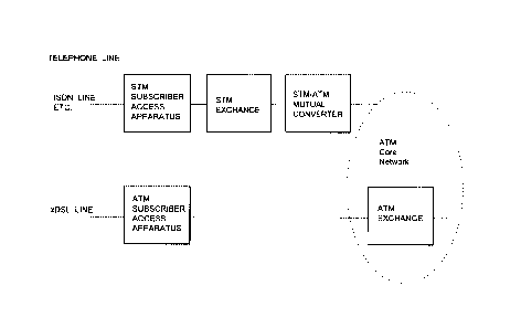
Fig. 1 shows an existing network environment including
STM and ATM subscriber access apparatuses;
Fig. 2 shows a relationship between ATM Core Network
and a subscriber access apparatus according to one aspect of
the present invention;
Fig. 3 is a block diagram of a subscriber access
apparatus according to one aspect of this invention;
CA 02272311 1999-OS-17
7
Fig. 4 is a block diagram of a subscriber access
apparatus according to an embodiment of the present
invention;
Fig. 5 shows a concrete example of the CLAD device
illustrated in Fig. 4;
Fig. 6 shows a concrete example of the ADSL-SLIC
illustrated in Fig. 4;
Fig. 7 shows a concrete example of the controller
illustrated in Fig. 4;
Fig. 8 shows the cell processing unit of the specific
CLAD device in Fig. 5; and
Fig. 9 shows a bloc diagram of a subscriber access
apparatus according to another embodiment of the present
invention.
Descri~t~on of the Preferred Embodiments:
Prior to detail description of embodiments of this
invention, brief description will at first made about an
existing network environment and an overview of the
embodiments of this invention.
Referring to Fig. 1, in an existing network environment,
an ATM subscriber access apparatus is connected to an xDSL
line which is included in an xDSL access network. On the
other hand, an STM subscriber access apparatus is connected
to an analog communication line of a telephone line, an ISDN
line, or the like. That is, subscriber access apparatuses
which are different in structure from each other should be
prepared each of the xDSL access networks and the others.
CA 02272311 1999-OS-17
8
Besides, since the STM subscriber access apparatus cannot be
directly connected to ATM Core Network, an STM exchange and
an STM-ATM mutual converter are required to connect the STM
subscriber access apparatus to the ATM Core Network.
On the other hand, a subscriber access apparatus
according to one aspect of the present invention accommodates
various lines each of which is connected to a telephone, a
facsimile, a terminal adapter ( TA ), an ISDN board installed
in a personal computer, an xDSL modem, such as an ADSL modem,
and so on. That is, the illustrated apparatus can handle
analog signals, ISDN data signals and xDSL signals, such as
ADSL signals.
Furthermore, the illustrated apparatus can be directly
connected to the ATM Core Network without other components.
That is, the apparatus shown in Fig. 2 can handles ATM cells.
Now, detail explanation of embodiments of this
invention will be made with reference to drawings, applying
an concept of this invention.
Referring to Figs. 2 and 3, a subscriber access
apparatus connects between the ATM Core Network on a upstream
side and local access networks on a downstream side, of the
analog communication access. network, the ISDN access network,
and the xDSL access network. That is, the illustrated
apparatus can adapt all of the analog communication access
network, the ISDN access network and the xDSL access network
to the ATM Core Network. Herein, the analog communication
access network has an analog communication line for analog
signals, the ISDN access network has an ISDN line for ISDN
CA 02272311 1999-OS-17
9
data signals including B-channel data signals, and the xDSL
access network has an xDSL line for xDSL signals. On the
other hand, the ATM Core Network transfers ATM cells thereon.
Herein, each ATM cell has a header and a payload.
The illustrated apparatus comprises an analog-SLIC 100,
an ISDN-SLIC 200, an xDSL-SLIC 300, a signal processor 400
and a controller 500.
The analog-SLIC 100 is connected to the analog
communication line and signal processor 400. Such analog-
SLIC 100 upwardly converts the analog signals into pulse code
modulation ( PCM ) signals to transmit the PCM signals into
the signal processor 400. On the other hand, the analog-SLIG
100 downwardly converts the PCM signals transmitted from the
signal processor 400 into the analog signals.
The ISDN-SLIC 200 connects between the ISDN line and
the signal processor 400. When receiving, on the downstream
side, the ISDN data signal from the ISDN line, the ISDN-SLIC
200 extracts the B-channel data signals from the ISDN data
signals to produce the B-channel data signals as digital data
signals. Such digital data signals of the B-channel data
signals are input into the signal processor 400. On the
other hand, the ISDN-SLIC 200 receives, on the upstream side,
the B-channel data signals as the digital data signals from
the signal processor 400 and then produces the ISDN data
signals having the B-channel data signals.
The xDSL-SLIC 300 is connected to the xDSL line and can
handle the xDSL signals, such as ADSL signals, VDSL signals,
HDSL signals, and SDSL signals.
CA 02272311 1999-OS-17
Such xDSL-SLIC 300 splits, on the downstream side, the
xDSL signals into high and low frequency data signals
referred to as fH and fL data signals in Fig. 3, respectively.
The high frequency data signals contain the high-speed
digital data, while the low frequency data signals contain
the POTS ( Plain Old Telephone Service ) data or speech data.
Herein, both of the high and low frequency data signals are
digital signals.
On the other hand, the xDSL-SLIC 300 produces the xDSL
signals corresponding to the high and low frequency data
signals transmitted from the signal processor 400 on the
upstream side.
The signal processor 400 is further connected to the
ATM Core Network and carries out signal-processing in
response to first and second control signals from the
controller 500.
In detail, the signal processor 400 processes, on the
downstream side, the PCM signals, the digital data signals
and the high and low frequency data signals in response to
the first control signal to output the ATM cells into the ATM
Core Network. Herein, into payloads of the ATM cells, the
PCM signals, the digital data signals and the high and low
frequency data signals are mapped.
On the other hand, the signal processor 400 processes,
on the upstream side, the ATM cells in response to the second
control signal to divide the ATM cells into the PCM signals,
the digital data signals, the high and low frequency data
signals. As mentioned above, the PCM signals, the digital
CA 02272311 1999-OS-17
11
data signals, high and the low frequency data signals are
transmitted into the analog-SLIC 100, the ISDN-SLIC 200 and
the xDSL-SLIC 300, respectively.
The controller 500 monitors the analog-SLIC 100, the
ISDN-SLIC 200, the xDSL-SLIC 300 and the signal processor 400.
Among them, if the signal processor 400 receives ATM cells
from ATM Core Network, then the controller 500 produces the
second control signal and outputs the signal into the signal
processor 400. On the other hand, if at least one of the
remaining components 100, 200 and 300 receives responding
signals, then the controller 500 produces the first control
signal and outputs the signal into the signal processor 400.
That is, the controller 500 produces the first control signal
in either case where the analog-SLIC 100 receives the analog
signals, case where the ISDN-SLIC 200 receives the ISDN data
signals, or case where the xDSL-SLIC 300 receives the xDSL
signals.
With this structure, the subscriber access shown in Fig.
3 can adapt all of the analog communication access network,
the ISDN access network and the xDSL access network to the
ATM Core Network.
Referring to Fig. 4, the above apparatus is applied to
the ADSL access network as the xDSL access network and
comprises, as the above signal processor 400, a time switch
410, a CLAD device 420 and an ATM network interface circuit
430. Herein, CLAD stands for cell assembly and disassembly.
With the direction to the ADSL access network as the
xDSL access network, the xDSL-SLIC is an ADSL-SLIC 310, the
CA 02272311 1999-OS-17
12
xDSL line is an ADSL line to be also connected, on a customer
site, to an ADSL modem in compliance with ANSI T1.413
standard, and the xDSL signals is an ADSL signals. That is,
the ADSL-SLIC 310 receives, on the downstream side, the ADSL
signals to produce the high and low frequency data signals
and receives, on the upstream side, the high and low
frequency data signals to produce the ADSL signals.
Additionally, the high frequency data signals is produced as
provisional ATM cells by the ADSL-SLIC 310 in this embodiment.
In addition, in this embodiment, the analog-SLIC 100
introduces, into the time switch 410, the PCM signals which
have 64 Kbps of data rate. The B-channel data signals,
namely the digital data signals, and the low frequency data
signals have 64 Kbps, respectively. The high frequency data
signals bypass the time switch 410 and directly input into
the CLAD device 420.
The illustrated time switch 410 receives, on the
downstream side, the PCM signals, the digital data signals
and the low frequency data signals all based 64Kbps of data
rates and makes upward switch-paths to produce intermediate
data signals in response to the first control signal. Herein,
the intermediate data signals contain the PCM signals, the
digital data signals and the low frequency data signals with
their order in time guaranteed. Furthermore, the
intermediate data signals are also 64Kbps-signals.
On the other hand, the time switch 410 receives, on the
upstream side, the intermediate data signals and makes
downward switch-paths to produce the PCM signals, the digital
CA 02272311 1999-OS-17
13
data signals and the low frequency data signals in response
to the second control signal.
The CLAD device 420 receives, on the downstream side,
the intermediate data signals based 64Kbps of data rate and
the high frequency data signals, and then assembles the ATM
cells in response to the first control signal. On the other
hand, the CLAD device 420 receives, on the upstream side, the
ATM cells and then disassembles the ATM cells to produce the
high frequency data signals and the intermediate data signals
in response to the second control signal. Herein, when the
CLAD device 420 receives the ATM cells transferred over
specific connection of VPI or VCI, the CLAD device 420
transmits their data into the controller 500, too. With this
function of the CLAD device 420, the controller 500 receives
control data from an upstream exchange ( not shown ), and
thereby, controls the time switch 410 and the CLAD device 420
in obedience to requests of the upstream exchange.
The ATM network interface circuit 430 is used in case
where, the ATM Core Network has an interface to be connected
to a synchronous optical network ( SONET ). Such ATM network
interface circuit 430 receives the ATM cells and maps the ATM
cells to the interface of the SONET. And thereby, the ATM
cells are transmitted into an upstream exchange not shown in
figure.
In detail, the CLAD device 420 may comprise an
intermediate data multiplexer/demulplexer 421, a cell
processing unit 422, an ATM header transfer 423 and an ATM
cell multiplexer/demultiplexer 424, as shown in Fig. 5.
CA 02272311 1999-OS-17
14
The illustrated intermediate data
multiplexer/demulplexer 421 multiplexes, on the downstream
side, the intermediate data signals to produce cell data
signals in response to the first control signal. On the
other hand, the intermediate data multiplexer/demultiplexer
421 demultiplexes, on the upstream side, the cell data
signals to produce the intermediate data signals in response
to the second control signal.
The cell processing unit 422 shown in Fig. 5 upwardly
processes the cell data signals to produce first ATM cells
and, on the other hand, downwardly processes the first ATM
cells to produce the cell data signals.
The ATM header translator 423 receives the provisional
ATM cells from the ADSL-SLIC 310 and upwardly translates
headers of the provisional ATM cells to produce second ATM
cells. On the other hand, the ATM header translator 423
receives, on the upstream side, the second ATM cells and
downwardly translates headers of the second ATM cells to
produce the provisional ATM cells.
The illustrated ATM cell multiplexer/demultiplexer 424
multiplexes, on the downstream side, the first and second ATM
cells to produce the ATM cells in response to the first
control signal. On the other hand, the ATM cell
multiplexer/demultiplexer 424 demultiplexes, on the upstream
side, the ATM cells into the first and second ATM cells in
response to the second control signal.
Referring to Fig. 6, the ADSL-SLIC 310 may comprise a
POTS splitter 311, a PCM processor 312 and an ATM cell
CA 02272311 1999-OS-17
generator 313.
The illustrated POTS splitter 311 splits, on the
downstream side, the ADSL signals into high and low frequency
analog signals and combines, on the upstream side, the high
and low frequency analog signals to produce the ADSL signals.
In detail, the POTS splitter 311 executes filtering process
to extract, as voice-data signals, only voice-band components
from the ADSL signals. The extracted voice-data signals
input into the PCM processor 312 as the low frequency analog
signals. Owing to this function, the POST splitter 311 is
also called a voice filter. On the other hand, the
remaining-band components of the ADSL signals pass through
the POTS splitter 311 into the ATM cell generator 313. For
example, such POTS splitter 311 comprises an analog filter,
such as a low-pass filter and a high-pass filter.
The PCM processor 312 shown in Fig. 6, upwardly
processes the low frequency analog signals to produce the low
frequency data signals. On the other hand, the illustrated
PCM processor 312 downwardly processes the low frequency data
signals to produce the low frequency analog signals. In this
embodiment, although the POTS splitter 311 and the PCM
processor 312 are discrete from each other, these components
may be integrated into one component.
The illustrated ATM cell generator 313 receives, on the
downstream side, the high frequency analog signals and
generates the provisional ATM cells as the high frequency
data signals corresponding to the high frequency analog
signals.
CA 02272311 1999-OS-17
16
Referring to Fig. 7, the controller 500 may comprise a
layer 1 controller, a LAPD controller, a switch controller, a
CLAD controller, a message controller and an ATM network
controller. Herein, LAPD stands for link access procedure.
The layer 1 controller controls the analog-SLIC 100,
the ISDN-SLIC 200 and the ADSL-SLIC 310 to allow access in
the Layer l, namely to establish the connection in the Layer
1. The LAPD controller controls the ISDN-SLIC 200 to
terminate D-channel of channels formed over the ISDN access
line.
In addition, the switch controller controls the time
switch 410 by producing the first and second control signals
indicative of making the upward and downward switch-paths,
respectively. The CLAD controller controls the CLAD device
420 by producing the first and second control signals
indicative of assembling the ATM cells and disassembling the
ATM cells, respectively.
Furthermore, the message controller controls the CLAD
device 420 to handle messages included in the ATM cells and
the ATM network controller controls the ATM network interface
circuit 430. In detail, the message controller carries out
message-conversion for the messages of the ATM cells, in
compliance with AAL protocol. Herein, AAL stands for ATM
adaptation layer and is recommended by ITU-T. In addition,
JP-A 6-276219 mentions about processing of AAL protocol and
is incorporated herein by reference.
The processor monitors the layer 1 controller, the LAPD
controller, the message controller and the ATM network
CA 02272311 1999-OS-17
17
controller to request that the switch controller and the CLAD
controller produce the first and second control signals in
correspondence with condition of the analog-SLIC 100, the
ISDN-SLIC 200, the ADSL-SLIC 310 and the ATM network
interface circuit 430.
In the above description, each SLIC accommodates only
one subscriber, since the switchover from one type SLIC to
another type SLIC can be carried out smoothly and unit of
maintenance can be decreased in size. However, this does not
restrict the scope of the present invention. That is, each
SLIC may accommodate a plurality of subscribers. Moreover,
though the above apparatus comprises only one ADSL-SLIC 310,
the apparatus may comprise a plurality of ADSL-SLICs 310.
The analog-SLICs 100 and the ISDN-SLICs 200 also.
Now, descriptions will made about operation of the
subscriber access apparatus more concrete than the above
description.
In this embodiment, since almost of the initialization
and the call/connection control for the apparatus all are
carried out by the upstream exchange of the ATM Core Network,
other initialization carried by the apparatus itself is only
to make condition that the apparatus, in question, can
receive requests from the upstream exchange.
Concretely, the apparatus executes the initialization
of itself as the followings: 1) Initial setting for the ATM
network interface circuit 430, 2) Setting the ATM cell
multiplexer/demultiplexer 424 to extract ATM headers
transmitted into the controller 500, and 3) Initialization
CA 02272311 1999-OS-17
18
about the message controller included in the controller.
In this circumstance, further settings about every
components in the apparatus are carried out, when the
apparatus receives control message indicative of
call/connection setting from the upstream exchange.
Concretely, the following setting are executed in response to
the control message:
1) Initializations of each SLICs. These
initializations may include establishments of connection in
the Layer 1. With these initializations, the controller
starts loop detection of the analog-SLIC 100, termination of
D-channel included in the ISDN data signals, monitoring call
requests for the ADSL-SLIC 310. If the controller 500
detects the variations of these SLICs, information signals
are transmitted from the controller 500 to the upstream
exchange through the CLAD device 420 and the ATM network
interface circuit 430.
2) Path-setting in the time switch 410. Detecting the
call request or the call accepted from a subscriber, the
upstream exchange requests to set the path in the time switch
410.
3) Setting to the CLAD device 420. When the
intermediate data signals input into the CLAD device 420, the
relationship between timeslot No. on the time switch 410 and
the headers of the ATM cells is established in the cell
processing unit 422. In addition, a table which is for use
in translating headers of the provisional ATM cells from
ADSL-SLIC 310, is set up for the ATM header translator 423.
CA 02272311 1999-OS-17
19
4) Additional setting to the CLAD device 420. In case
of necessity, priority is set up for the ATM cell
multiplexer/demultiplexer 424 so that the ATM cells are
multiplexed in compliance with the priority to be transmitted
into the ATM network interface circuit 430.
After the above settings, the analog signals, the ISDN
data signals and the ADSL signals are handled as described in
below.
1) As mentioned above, the analog signals, the ISDN
data signals and the ADSL signals are processed by the
analog-SLIC 100, the ISDN-SLIC 200 and the ADSL-SLIC 310, and
then, the PCM signals, the digital data signals and the low
frequency data signals are transmitted into the time switch
410. The time switch 410 receives these signals, and then,
transmits the intermediate data signals into the CLAD device
420. In the CLAD device 420, the intermediate data signals
are multiplexed by the intermediate data
multiplexer/demultiplexer 421, and then, their content data
are mapped into payloads of the first ATM cells. Herein, the
mapping is compliance with the above relationship set up by
the controller 500. In addition, if voice data has 64I~ps of
data rate, 6 msec ( = 125 a sec x 48 ) in time are required in
order to map the voice data into payloads of the ATM cells,
each of which has 48 Byte. The ATM cell
multiplexer/demultiplexer 424 multiplexes the first and
second ATM cells in compliance with priority controlled by
the controller 500. Herein, other ATM cells from the
controller 500 may be also multiplexed, if necessary. The
CA 02272311 1999-OS-17
ATM cells multiplexed by the multiplexer 424 are input into
the ATM network interface circuit 430, and then, are
introduced into the ATM Core Network.
2) On the other hand, when the ATM cells which have
voice data and are output from the upstream exchange, are
transmitted into the CLAD device 420 through the ATM network
interface circuit 430, the ATM cell multiplexer/demultiplexer
424 identifies the ATM cells including voice data, according
to the header thereof. The identified ATM cells are
introduced into the cell processing unit 422. The cell
processing unit 422 picks voice data up from the payloads of
the ATM cells and transmits into the timeslots, based on the
control of the controller 500.
3) In the CLAD device 420, when the high frequency data
signals as the provisional ATM cells from the ADSL-SLIC 310
are input, and then the ATM header translator 423 translates
the header of the provisional ATM cells and produces the
second ATM cells to be transmitted into the ATM cell
multiplexer/demultiplexer 424. Following operations are as
the same operation of voice data.
Referring to Fig. 8, the cell processing unit 422 may
comprise a speech coding unit 425, an AAL 2 processor 426 and
an AAL 1 processor 427. Herein, AAL 1 is used for
connection-oriented, delay-sensitive services requiring
constant bit rates, such as uncompressed video and other
isochronous traffic, while AAL 2 is used for connection-
oriented services that support a variable bit rate, such as
some isochronous video and voice traffic. AAL 1 and AAL 2
CA 02272311 1999-OS-17
21
are recommended as I.363.1 and 1.363.2 by the ITU-T.
In detail, the speech coding unit 425 receives ones of
the cell data signals from the intermediate data
multiplexer/demultiplexer 421 and carries out high-efficiency
speech coding to produce coded data signal. For example, the
speech coding unit 425 may be complied with recommendation of
ITU-T G series and may carry out coding of voice data or
speech data. By such coding, the voice data are compressed
so that the amount of data becomes 32Kbps ~ BKbps and, as a
result, high-efficiency data transmission is achieved.
The AAL 2 processor 426 is complied with ITU-T I.363.2
and processes the coded data signal to produce ones of the
first ATM cells. Thus, AAL protocol is applied to the above
processing so that a plurality of short cells can be inserted
in the ATM cells which have common headers on the ATM Core
Network, and thereby, lines can be effectually used.
The AAL 1 processor 427 is complied with ITU-T I. 363.1
and processes others of the cell data signals to produce
others of the first ATM cells.
Referring to Fig. 9, a subscriber access apparatus
according to another embodiment of this invention is a
modification of the above embodiment illustrated in Fig. 4.
Thus, description of this embodiment will be directed only to
a difference between the above embodiment and this one.
In such apparatus, the signal processor comprises a
signal multiplexer/demultiplexer 440, the CLAD device 420 and
the ATM network interface circuit 430. That is, in this
embodiment, the time switch 410 in Fig. 4 is replaced by the
CA 02272311 1999-OS-17
22
signal multiplexer/demultiplexer 440.
The illustrated signal multiplexer/demultiplexer 440
receives, on the downstream side, the PCM signals, the
digital data signals and the low frequency data signals to
produce the intermediate data signals in response to the
first control signal. On the other hand, the signal
multiplexer/demultiplexer 440 receives, on the upstream side,
the intermediate data signals to produce the PCM signals, the
digital data signals and the low frequency data signals in
response to the second control signal.
Such signal multiplexer/demultiplexer 440 can be
obtained by fixing all paths in the time switch 410
illustrated in Fig. 4. In this event, switching function is
achieved in the CT_An device. This application makes the
structure of the apparatus simple.
Moreover, this invention also provides the method of
use of the above apparatus as another aspect thereof.
The ATM network has a large amount of data transmission
capacity. On the contrary, an amount of data transmission
capacity of telephone subscriber lines and ISDN lines is much
smaller than one of the ATM network, because capacity per one
analog line is only 64 Kbps. For example, if the number of
telephone subscriber lines is equal to 100, their
transmission capacity becomes only 6Mbps ( = 64Kbps x 100
lines ). Besides, the number of lines is restricted to
predetermined number, for example 200, and cannot be
increased much, because of the role of the subscriber access
apparatus in network architecture.
CA 02272311 1999-OS-17
23
On the other hand, the high frequency data signals of
the ADSL signals have about 40 Mbps at maximum. Therefore,
an increase of such ADSL signals can contribute an efficiency
use of the ATM network. For the purpose, it is proposed that
the ATM cell multiplexer/demultiplexer 424 assign a suitable
band to each SLIC of different types. The combination of the
suitable bands causes an efficiency use of the ATM
transmission capacity.