Language selection

Search

Patent 2272656 Summary

Third-party information liability

Some of the information on this Web page has been provided by external sources. The Government of Canada is not responsible for the accuracy, reliability or currency of the information supplied by external sources. Users wishing to rely upon this information should consult directly with the source of the information. Content provided by external sources is not subject to official languages, privacy and accessibility requirements.

Claims and Abstract availability

Any discrepancies in the text and image of the Claims and Abstract are due to differing posting times. Text of the Claims and Abstract are posted:

  • At the time the application is open to public inspection;
  • At the time of issue of the patent (grant).
(12) Patent Application: (11) CA 2272656
(54) English Title: COMB FILTER
(54) French Title: FILTRE EN PEIGNE
Status: Deemed Abandoned and Beyond the Period of Reinstatement - Pending Response to Notice of Disregarded Communication
Bibliographic Data
(51) International Patent Classification (IPC):
  • H03H 17/04 (2006.01)
  • H03H 17/02 (2006.01)
(72) Inventors :
  • DRAXELMAYR, DIETER (Austria)
(73) Owners :
  • SIEMENS AKTIENGESELLSCHAFT
(71) Applicants :
  • SIEMENS AKTIENGESELLSCHAFT (Germany)
(74) Agent: SMART & BIGGAR LP
(74) Associate agent:
(45) Issued:
(86) PCT Filing Date: 1998-08-21
(87) Open to Public Inspection: 1999-04-01
Examination requested: 2001-05-09
Availability of licence: N/A
Dedicated to the Public: N/A
(25) Language of filing: English

Patent Cooperation Treaty (PCT): Yes
(86) PCT Filing Number: PCT/DE1998/002453
(87) International Publication Number: WO 1999016169
(85) National Entry: 1999-05-21

(30) Application Priority Data:
Application No. Country/Territory Date
19741922.4 (Germany) 1997-09-23

Abstracts

English Abstract


The invention relates to a comb filter consisting of integrators (I1, I2, I3)
connected in series, to which a digital data flow with high scanning rate is
fed in order to supply a digital data flow with a lower scanning rate. The
most significant bits of the digital data flow are reset in the first and
second integrators (I1, I2), whereby the resetting of the bits in the first
integrator (I1) is stored in a counter (Z). The count of the counter (Z) is
fed to the most significant bits of the last integrator (I3) during reset time.


French Abstract

L'invention concerne un filtre en peigne constitué d'intégrateurs (I1, I2, I3) montés en série, auxquels est conduit un courant de données numérique, à une haute fréquence d'échantillonnage, pour produire un courant de données numérique à une fréquence d'échantillonnage plus basse. Les bits de poids fort du courant de donnée numérique sont remis à zéro dans le premier et dans le second intégrateur (I1, I2), la remise à zéro des bits dans le premier intégrateur (I1) étant mémorisée dans un compteur (Z). L'état du compteur (Z) est entré, au moment de la remise à zéro, dans les bits de poids fort du dernier intégrateur (13).

Claims

Note: Claims are shown in the official language in which they were submitted.

claims
1. A comb filter comprising at least three series connected
integrators (I1, I2, I3), to which is fed a digital data stream at
a high sampling rate in order to yield a digital data stream at a
low sampling rate,
characterized
in that the most significant bits of the digital data stream
can be reset in the integrators (I1, I2), in that it is possible
to store the resetting of the bits in the first integrator (I1) in
a counter (Z), and in that the counter reading of the counter (Z)
can be fed selectively into at least one bit of the last
integrator (23) at the reset time.
2. The comb filter as claimed in claim 1,
characterized
in that the counter reading of the counter (Z) can be fed
into the most significant bite of the last integrator (I3) at the
reset time.
3. The comb filter as claimed in claim 1,
characterized
in that the last integrator (I3) simultaneously acts as a
differentiator.
4. The comb filter ae claimed in one of the preceding claims,
characterized
in that a correction value can be fed into the most
significant bits of the last integrator (I3).
5. The comb filter as claimed in claim 4,
characterized
in that the correction value can be fed in via the counter
(7).
6. The comb filter as claimed in one of the preceding claims,
characterized
in that the integrators (91, 92, 93) are designed as
counters.

Description

Note: Descriptions are shown in the official language in which they were submitted.


05/18/1999 11:53 9549251101 LERNER AND GREENBERG PAGE 02
' . FILE, Pdld-dt~TNIS ~iit~:' ~:.g;~.
Descx-iption ~-TRANSLATION
Comb filter
The irxvention re~.ates to a comb filter comprising series connected
integrators, to which is fed a digital data stream at a high
samp~.ing rate in order to yield a digital data stream at a low
sampling rate.
So called decimation filters are used to convert a digital data
stream having a high sampling rate into a data stream having a low
sampling rate. The filter function of such decimation filters
usually has low pass filter properties and effects an increase in
the word width of the data decimated by the decimat~.on filter. A.
bit stream at a high sampling rate can thus be decimated into, for
example, 16 bit words in the voice band.
One field of application is digital telephony. Tn this case) at
least one such decimation filter is connected downstream of a
Sigma Delta analog/digital converter.
The decimation factor of a decimatiorx ;filter is usually determined
by a power of two, that is to say 2, 4, 16, 64, etc. The usual
structure for such a decimation fi~,tex' is afforded by a comb
filter, since a filter of the ~.atter type can be realized with a
x'eZatively low outlay.
Fig. 2 shows an e7cample of a known comb or decimation filter, in
which three so called Dump integrators I (I1, I2, I3) in each case
with a summation element S and a delay e7.ement V in the feedback
path are conxiected in a cascade and are reset after N clock cycles
in each case via the associated delay element v, which is
indicated by "reset N". The respective word width ml and mz and m3
of the output data stream of the summation elements S can be
adapted to the Dump integrators T.
transversal superposition stage TS comprising further summation
elements, delay elements V having an L~ fold delay and muZtip~.iers
M is connected downstream of the cascade circuit comprising
integrators I, N deaignatixzg the summation factor.
The object of the present invention is to provide a comb filter
which is suitable as a decimation filter and is distinguished by a
simp~.e structure.
Tn the case of a comb filter of the type mentioned in the
introduction, this object is achieved according to the invention
by virtue of the fact that the most significant bits of the
digital data stream can be reset in the integrators, that it is
possible to store the resetting of the bits in the first
integrator ixi a counter, and that the Counter reading of the
CA 02272656 1999-OS-21

05/18/1999 11:53 9549251101 LERNER AND GREENBERG PAGE 03
counter can be fed into at least one bit, preferably the most
significant bits, of the last integrator at the reset time.
The invention has the advantage that a reset error appears as a
multiple of a power of two in subsequent stages, with the result
that it can be corrected in a particularly simple manner in the
subsequent stages.
In this case, the number of integrators is not limited in
principle, although three integrators are sufficient in many
applications. correspondingly, reference is made below to
exemplary embodiments having three integrators, i.e. third order
filters.
In the case of the comb filter according to the invention, unlike
in the l~xloWrl comb filter of Fig. 2, therefore, the reset signal is
not passed to the integrators in their entirety) rather a.s applied
only to the mpst significant bits. 'fhe result of this is that just
a simple counter is required as arithmetic unzt for the correction.
of the reset errors. In particular, the last integrator - and that
is to say the third integrator in the case of a three stage
arrangement - is preset not to zero but to a value determined by
the counter.
The reasons for this shall be explail2ed in more detail below:
A third order comb filter with a decimation factor of 256 (2n8)
has a number range from zero to 256n3. Tf the representation of
256n3 is then dispensed with and the value Zero is accepted for
this, then 24 bits are neces~saxy for a representation. 25 bits
wou~.d be requ~.red in the case of a representation of 256n3, which
means that the following considerations shift by 1 bit.
Computation,a~. errors modulo 256n3 accordingly are not noticeable
and can be ignored. Thus, a computational accuracy of 24 bits
suffices in order to obtain an exact result.
Tf an error fJ. occurs in the first integrator at a particular
time, which may happen as a result of resetting, for example, then
this error is evaluated after 256 clock cycles at the output of
the third integrator, where the error is then f3 - t1.*256*257/2 =
fl*12s*(256 + 1). If the error fl amounts to a*512, for example,
then f3 - a*512*128*256 + a*512*128 is produced. In other words,
a*256n2 when considered modulo 256n3.
This means the following:
If the third integrator ie set not to the vs,~,ue zero but to the
value -a*256~256, then the error fl is compensated for. The same
applies correspondingly not just to 2S6 Clock cycles but also to
CA 02272656 1999-OS-21

05/18/1999 11:53 9549251101 LERNER AND GREENBERG PAGE 04
any desired multiples thereof. The reason is that the third
integrator simultaneously operates as a differentiator as well,
and that when the accumulating values are differentiated, -
a*256*256 is always present as the result.
In this case, the value of a is produced as follows: In the first
integrator, the bit with the significance of 512 is reset at the
reset time. If said bit previously had the value 1, then the error
f1 specified above is produced exactly. This error is added to the
preceding errors that occurred correspondingly. Therefore, the
error counter of the first integrator is simply incremented in
this case. This error counter loads, in turn, the Last or third
integrator. The negative sign disappears because a is usually
negative, since the error arises when a bit is reset.
zn order) furthermore, to prevent the occurrence of any further
errors, the first integrator must always have a width of 10 bits.
The error counter, which is connected downstream of the first
integrator, comprises multiples of 256n2 and must accordingly have
a width of a bits, since an overall computational accuracy of 24
bits is presupposed. That is to say that a esmall~~ counter is
sufficient.
Therefore) values up to a maximum of 767 Come from the first
integrator. In 256 clock cycles, this value can accumulate to at
most values of less than/equal to 767*256 - 196352. The start
value of the second integrator is less than 2n16, with the result
that a word width of 18 bits is sufficient to avoid an
uncontrolled overflow. At the reset time, a11 bits which symbolize
2n16 and multiples thereof can be erased because, after 256 clock
cycles, the accumulative error in the third integrator hoe the
value 2n24 ox a multiple thereof and, therefore, need not be taken
into account. That is to say that the start value after resetting
is in the second integrator, in other words has values which are
less than 2n16, as has already been assumed above.
overall, the comb filter according to the invention therefore
operates in the following manner.
Synchronous resetting of the most significant bits is performed by
1 bit in the first integrator and by 2 bits in the second
integrator. In this case, the resetting of the bits in the first
integrator is stored in an error counter which is connected
downstream of the first integrator and has a word width of 8 bits.
The counter reading thus determined is then fed into the moat
significant bits of the last or third integrator) which
simultaneously acts as a differentiator, at the reset time. The
lees significant bits of the last or third integrator are reset in
a customary manner, further Computational steps not being
necessary.
CA 02272656 1999-OS-21

05/18/1999 11:53 9549251101 LERNER AND GREENBERG PAGE 05
The invention thus provides a comb filter which is constructed in
a simple manner, can be realized with a low outlay and Can
reliably Convert a digital data stream having a high sampling rate
into a digital data stream having a lower sampling rate.
The invention is explained iri more detail below with reference to
the drawings of an exemplary embodiment illustrated in the
drawing, in which:
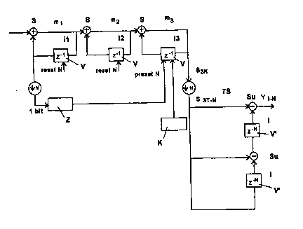
Fig. 1 shows a block diagram of a comb filter according to the
invention, and
Fig. 2 shows a block diagram of a conventional comb filter.
Fig. 2 has already been explained above. The same reference
symbols as in Fig. 2 are used for corresponding parts in Fig. 1.
In Fig. 1, three integrators, I1, I2 and T3, with summers S are
arranged in a cascade as in Fig. 2, it being possible for the
respective word width ml, m2 and m3 to be adapted to these
integrators I1, 2~ and I3. In contrast to the existing comb filter
in accordance with Fig. 2, in the case of the comb filter
according to the invention, a Counter Z having a word width of $
bits is connected downstream of the integrator I1, which Counter
cQUnts the resetting of the bits in the integrator I1. The counter
reading thus determined in the counter Z is then fed into the most
significant bits of the third integrator I3, which simultaneously
acts as a differentiator, at the reset time, while the less
significant bits of the third integrator I3 are reset in a
Customary manner. The entire delay element is reset; selective
resetting is not provided.
Tn the case of the cascade circuit comprising the integrators I1,
I2 and I3, a transversal superposition stage PS comprising
SubtraCtors Su arid integrators I is once again connected
downstream.
A Correction value which Can be chosen as desired and is stored in
a register K may optionally be input into the third integrator I3
via said register K.
As the simplest design of an integrator I, it is possible to use a
counter for this purpose. That is because, for example, a maximum
of one bit can be added in the first integrator at each time Step,
which corresponds to a counter step of 1. This also applies t¢
more significant bits in the downstream integrators, since only
the overflows of the less significant bits are fed in there.
CA 02272656 1999-OS-21

Representative Drawing
A single figure which represents the drawing illustrating the invention.
Administrative Status

2024-08-01:As part of the Next Generation Patents (NGP) transition, the Canadian Patents Database (CPD) now contains a more detailed Event History, which replicates the Event Log of our new back-office solution.

Please note that "Inactive:" events refers to events no longer in use in our new back-office solution.

For a clearer understanding of the status of the application/patent presented on this page, the site Disclaimer , as well as the definitions for Patent , Event History , Maintenance Fee  and Payment History  should be consulted.

Event History

Description Date
Application Not Reinstated by Deadline 2004-08-23
Time Limit for Reversal Expired 2004-08-23
Deemed Abandoned - Failure to Respond to Maintenance Fee Notice 2003-08-21
Amendment Received - Voluntary Amendment 2003-05-05
Amendment Received - Voluntary Amendment 2001-06-11
Letter Sent 2001-05-30
All Requirements for Examination Determined Compliant 2001-05-09
Request for Examination Received 2001-05-09
Request for Examination Requirements Determined Compliant 2001-05-09
Inactive: Cover page published 1999-08-16
Inactive: IPC assigned 1999-07-19
Inactive: First IPC assigned 1999-07-19
Letter Sent 1999-06-23
Inactive: Notice - National entry - No RFE 1999-06-23
Application Received - PCT 1999-06-22
Application Published (Open to Public Inspection) 1999-04-01

Abandonment History

Abandonment Date Reason Reinstatement Date
2003-08-21

Maintenance Fee

The last payment was received on 2002-08-06

Note : If the full payment has not been received on or before the date indicated, a further fee may be required which may be one of the following

  • the reinstatement fee;
  • the late payment fee; or
  • additional fee to reverse deemed expiry.

Please refer to the CIPO Patent Fees web page to see all current fee amounts.

Fee History

Fee Type Anniversary Year Due Date Paid Date
Basic national fee - standard 1999-05-21
Registration of a document 1999-05-21
MF (application, 2nd anniv.) - standard 02 2000-08-21 2000-07-18
Request for examination - standard 2001-05-09
MF (application, 3rd anniv.) - standard 03 2001-08-21 2001-08-10
MF (application, 4th anniv.) - standard 04 2002-08-21 2002-08-06
Owners on Record

Note: Records showing the ownership history in alphabetical order.

Current Owners on Record
SIEMENS AKTIENGESELLSCHAFT
Past Owners on Record
DIETER DRAXELMAYR
Past Owners that do not appear in the "Owners on Record" listing will appear in other documentation within the application.
Documents

To view selected files, please enter reCAPTCHA code :


To view images, click a link in the Document Description column. To download the documents, select one or more checkboxes in the first column and then click the "Download Selected in PDF format (Zip Archive)" or the "Download Selected as Single PDF" button.

List of published and non-published patent-specific documents on the CPD .

If you have any difficulty accessing content, you can call the Client Service Centre at 1-866-997-1936 or send them an e-mail at CIPO Client Service Centre.


Document
Description 
Date
(yyyy-mm-dd) 
Number of pages   Size of Image (KB) 
Representative drawing 1999-08-13 1 6
Cover Page 1999-08-13 1 38
Abstract 1999-05-21 1 58
Description 1999-05-21 4 233
Claims 1999-05-21 1 33
Drawings 1999-05-21 2 28
Notice of National Entry 1999-06-23 1 194
Courtesy - Certificate of registration (related document(s)) 1999-06-23 1 116
Reminder of maintenance fee due 2000-04-26 1 111
Acknowledgement of Request for Examination 2001-05-30 1 178
Courtesy - Abandonment Letter (Maintenance Fee) 2003-09-18 1 176
PCT 1999-05-21 4 106