Note: Descriptions are shown in the official language in which they were submitted.
CA 02273324 1999-OS-20
WO 98/18296 PC'Ti:~L~9610067()
A POWER CONTROL APPARATUS FOR LIGHTING SYSTEMS
This invention relates to a power control apparatus which is particularly
useful for lighting
systems, such as those employing fluorescent lights.
Studies have shown that many buildings, for example, tend to be over
illuminated by present
lighting systems for the purposes required of them. Over illumination in this
way results in
a wastage of electrical power. Most often fluorescent lights are used in
lighting systems for
large buildings, for example, in view of their increased efficiency as
compared to many other
lights. Also, the relationship between light output and power required in a
fluorescent light
is non-linear, and it has been found that a significant decrease in power
usage by fluorescent
lights can be achieved without a correspondingly noticeable change in light
output in many
instances. However, if reduced power is continuously supplied to a fluorescent
lighting
system, the lights may experience starting difficulties, such as increased
flickering time, which
can reduce the life span of the lights. Furthermore, it may be desired to
adjust the light level
output of the lights, and in a large lighting system installation it may be
desired to alter the
light output or the power consumed thereby from a remote or centralised
location.
In accordance with the present invention there is provided a power control
apparatus for
lighting systems comprising:
a power variation means coupled to receive an input power source of AC
electricity
and produce a controllable output power source of AC electricity for operating
an electrical
Load comprising at least one light;
monitoring means for monitoring electrical parameters of the input power
source
and/or the output power source to produce monitoring signals;
a digital processing means coupled to receive said monitoring signals and
coupled to
said power variation means so as to control said power variation means to vary
said output
power source between a maximum output level and a minimum output level;
a timer coupled to said digital processing means; and
a first memory storing control parameters and coupled to said digital
processing
CA 02273324 1999-OS-20
WO 98/18296 PCTIAU96/00670
means;
wherein said digital processing means is responsive to a condition of said
monitoring
signals to control said power variation means to produce said output power
source at a first
predetermined level for a predetermined time period and thereafter to reduce
said output
power source to a second predetermined level, and wherein said second
predetermined level
and said predetermined time period are set by said digital processing means
according to the
control parameters stored in said first memory.
Preferably said stored control parameters include indications of predetermined
times of day
and/or days of week and corresponding values for said second predetermined
level, and
wherein said digital processing means is responsive to said timer at said
predetermined times
of day and/or days of week to change said second predetermined level to the
corresponding
value stored in said memory.
In a preferred form of the invention, at least one light sensor is coupled to
the digital
processing means, and the digital processing means is also responsive to a
light level detected
by the at least one light sensor to increase or decrease the second
predetermined level. In one
form of the invention, the apparatus includes a plurality of light sensors
coupled to said digital
processing means, each producing a respective detected light level value, and
wherein said
digital processing means is operative to calculate a weighted average of the
detected light
level values on the basis of preselected respective weighting factors stored
in said memory,
said digital processing means being responsive to the weighted average to
increase or decrease
said second predetermined level.
Preferably, the apparatus further comprises an input port coupled to the
digital processing
means for receiving control commands, wherein said digital processing means is
responsive
to a first control command to change said stored control parameters including
said second
predetermined level.
Preferably, a second memory is also provided coupled to the digital processing
means for
CA 02273324 1999-OS-20
WO 98/18296 PCT/AU96/00670
storing performance data, and wherein for each power variation in said output
power source
said digital processing means stores performance data in said second memory.
The
performance data may include data representing the output level of said output
power source
and the time the power variation occurred.
In one form of the invention a plurality of power variation means are provided
coupled to a
single digital processing means, with each power variation device being
arranged to supply
its output power source to a corresponding different electrical load. In this
configuration, the
digital processing means is preferably adapted to control each of the power
variation means
separately according to different corresponding second predetermined levels.
Various forms of power variation means may be utilised in the invention. For
example, the
power variation means may comprise a variable transformer, wherein said first
predetermined
level corresponds to a larger AC voltage than said first predetermined level.
Alternatively,
the power variation means may comprise, for example, a waveform modification
device, such
as a silicon controlled rectifier (SCR), wherein the difference between the
first and second
predetermined levels is effected by varying the firing time of the SCR with
respect to the
voltage zero crossing point of the AC electricity input power source.
In a preferred form of the invention, said power variation means comprises a
variable
transformer, and wherein said first predetermined level corresponds to a
larger AC voltage
than said second predetermined level. Preferably, said monitoring means
monitors line
voltage and/or line current of said input power source in order to determine
the zero crossing
times thereof, and wherein said digital processing means is adapted to control
said power
variation means to vary the output power source only at least substantially at
a said zero
crossing time.
As can be determined by those skilled in the art from the present
specification, embodiments
of the invention provide for a power control apparatus which can be utilised
to reduce power
consumption of an electrical load such as a fluorescent lighting system. When
a condition
such as the turning on of fluorescent lights is detected by the monitoring
means, the preferred
CA 02273324 1999-OS-20
WO 98I18Z96 PCT.~.aU961o067o
-4-
power control apparatus responds by increasing the output power source to a
first
predetermined level (eg maximum available power) in order to facilitate
starting of the lights.
After a predetermined time period the output power source is then reduced to a
second
predetermined level in order to conserve electrical power. The second
predetermined level
and thus the amount of power saving, is adjustable by way of an input port for
recei~.~ing power
control commands. The second predetenmined level may also be adjusted by the
influence of
other inputs, such as at selected times of the day, or in response to a light
sensor which
measures ambient light.
l 0 The invention is described in greater detail hereinafter by reference to
several embodiments
thereof illustrated by way of example in the accompanying drawings, wherein:
Figure 1 is a block diagram of a power control apparatus according to a first
embodiment;
Figure 2 is a block diagram of a power control apparatus according to a second
embodiment;
Figure 3 is a block diagram of a power control apparatus according to a third
embodiment;
Figure 4 is a functional flow diagram illustrating an algorithm for
controlling a
microprocessor device in an embodiment of the invention;
Figure 5 is a block diagram illustrating a further embodiment of the
invention;
Figure 6 illustrates an example of a power device for use in embodiments of
the
invention; and
Figure 7 is a timing diagram.
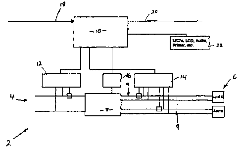
A power control apparatus 2 is illustrated in Figure 1 in block diagram form,
coupled between
a mains AC electrical input power source 4 and one or more electrical loads 6,
such as a
fluorescent or discharge lighting system, or the like. The power control
apparatus 2 comprises
generally a power variation means in the form of power device 8, and a digital
processing
means embodied in microprocessor circuit 10. The power device 8 is coupled to
receive the
CA 02273324 1999-OS-20
WO 98/18296 1'CT/:~U96/00670
-5-
mains electrical input power source 4, and provides at least one output power
so~:rce 9
providing power to the at least one load 6. Monitoring circuitry 12, 14 is
provided for
monitoring electrical parameters of the mains electrical input power source 4
and output power
sources 9, respectively. As shown diagrammatically in Figure 1, each of the
monitoring
circuits 12, 14 receive signals which are indicative of voltage and current
flow of the input and
output power sources, respectively, and provide input to the digital
processing circuit 10.
Thus, as will be apparent to those skilled in the art, each of the monitoring
circuits 12, 14
advantageously includes appropriate signal filtering and conditioning
circuitry, and conversion
circuitry for providing inputs to the digital processing circuit 10 in
appropriate signal levels
and formats, indicative of the voltages and currents monitored. Analog-to-
digital conversion
circuitry is also included in the monitoring circuits 12, 14 in order to
provide the appropriate
inputs to the digital processing circuit 10.
The power device 8 primarily provides a means for varying the power supplied
to the
I 5 electrical loads 6 through each of the output power sources 9. Several
methods of varying the
power supplied to the output power sources 9 are applicable, and the
particular form of the
power device 8 will depend upon the power variation method employed. For
example, one
way of reducing the power utilised by a load 6 is to supply the load at a
reduced voltage. In
that case, the power device 8 may comprise a vultage reduction transformer,
and it is preferred
that the transformer output voltage be capable of variation between at least
100% of input
voltage down to a fraction of the input voltage such as 50%. This can be
achieved through the
use of, for example, an auto-transformer of conventional form, which has a
plurality of
voltage taps or is continuously variable. In order to vary the output voltage
of the auto-
transformer, the output tap is moved from one connection to another which,
depending upon
the physical characteristics of the transformer, can be achieved mechanically
or through
electrical switching. It will be readily apparent to those skilled in the art
that the switching or
mechanical movements, such as by way of stepper motor, required in order to
vary the output
voltage can be achieved by conventional means, and thus the details of
implementation are not
included here so as to avoid clouding the clarity of description of the
invention.
CA 02273324 1999-OS-20
WO 98118296 PCT/AU96/Oa67t)
-6-
Another way in which the power output of the power device can be varied from
the input
power source level is through the use of waveform modification such as may be
achieved
utilising a silicon controlled rectifier (SCR) or thyristor circuit. In that
case, the level of
output power from the power device can be varied by varying the firing time of
the SCR or
thyristor. By increasing the firing time with respect to the zero crossing
point of the source
power input voltage waveform, it is possible to vary the power delivered to
the load 6 at the
output of the power device 8. The manner in which the firing time of a
waveform
modification circuit of the type described will also be readily apparent to
those skilled in the
art, and thus is not described in detail.
The power device 8 is coupled to the digital processing circuit 10 by way of a
power control
circuit 16. The function of the power control circuit 16 is primarily to
receive control signals
from the digital processing circuit 10 and translate those signals into the
form required for
controlling the power variation of the power device 8. For example, where the
power device
8 comprises a continuously variable auto-transformer whose output is
controlled mechanically
through the use of a stepper motor or the like, the power control circuit 16
is adapted to
translate logic level control signals output from the digital processing
circuit 10 into electrical
signals for operating the stepper motor so as to vary output of the power
device 8. On the
other hand, for different embodiments of the power device 8, the power control
circuitry 16
may not be required, or may be incorporated in the digital processing circuit
circuit 10. For
example, if the power device 8 comprises waveform modification circuitry such
as SCRs
which require only logic level signals which are timed accurately, then those
firing signals
may be provided directly from the digital processing circuit 10.
The digital processing circuit 10 may comprise any suitable digital processing
circuitry, such
as a microprocessor or mierocontroller circuit or the like having provision
for input and output
of signals, and memory for storing control algorithms and data. For example,
an 8251
microcontroller circuit, which will be recognised by those of skill in the
art, can be effectively
utilised in the digital processing circuit 10. As mentioned, the digital
processing circuit 10
receives input signals from the monitoring circuits 12 and 14, and outputs
control signals to
CA 02273324 1999-OS-20
WO 98/18296 YCTIAU96/00670
the power device 8 by way of the power control circuitry 16. The digital
processing circuit
is also provided with a programming input port 18, an output data port 20, and
optionally
is coupled to one or more display devices 22.
5 The digital processing circuit 10 includes processing circuitry which
functions under the
control of instructions stored in a memory circuit, preferably a non-volatile
form of memory,
such as ROM, PROM, EPROM, flash RAM or battery backed RAM. The circuit 10 is
also
provided with memory such as RAM memory for storing control parameters (which
may be
received from the programming port 18) and storing data to be output by way of
the output
10 port 20 or display device 22. The primary function of the digital
processing circuit 10 is to act
in accordance with its programmed instructions and control parameters, and on
the basis of
inputs received from the monitoring circuits 12, 14 and programming input port
18, so as to
control the power device 8, and in particular the output power directed to the
loads 6 through
output power sources 9. Figure 4 illustrates an example of a control algorithm
for the
microprocessor control circuit 10. The algorithm illustrated in the flow chart
diagram of
Figure 4 in practice would be embodied in instruction codes stored in memory
and executed
by the microprocessor or microcontroller, although in an alternative the
digital processing
circuitry 10 could comprise a programmable logic circuit (PLC) or the like, in
which case the
algorithm may be hard wired into the PLC. As mentioned, in addition to memory
storage for
the control instructions, the digital processing circuit 10 preferably also is
provided with
memory storage for control parameters which may be received, for example, by
way of the
programming port 18. The control parameter data stored in the digital
processing circuit 10
would typically include:
data indicative of a reduced operating power level for the loads coupled to
the control
apparatus;
the number of steps between the reduced operating power level and the full
operating
power level where the power device 8 is variable in discrete steps;
the time delay, when new load is added, to remain at full output power level
before
decrementing to the reduced output power level;
a threshold value indicating the amount of new load that must be added for the
output
CA 02273324 1999-OS-20
WO 98/18296 PC'T/At196/00670
_g_
power source to be switched to full output power; and
the time interval to remain at each step where the power level varies in
discrete steps
or, where the power level is continuously variable, the total time to reduce
the power
level from the full output level to the reduced output level.
Referring to Figure 6, there is illustrated a simplified diagram of an auto-
transformer 40
which may be utilised in the power device 8 of embodiments of the present
invention. The
auto-transformer 40 is configured to receive mains input voltage Va,, at the
primary terminals
thereof, and has a plurality of taps labelled P~ to P6 for secondary
terminals. The taps P, to P6
are coupled to respective inputs of a multiplexing circuit 42 which has a
single output 44
which provides an output voltage Vo~.i.. The multiplexing circuit 42 is
constructed so as to
couple one and only one of the inputs thereof to the output 44, in accordance
with a command
input 46, provided in practice from the digital processing circuit 10.
I 5 By way of example, the taps P, to P6 may be arranged so as to enable
variation of the output
voltage o~.,. within the range of 100% Vu,, to 50% Vu,, in 10% increments.
Accordingly, the
output voltage and consequently the output power supplied to the load, can be
varied by
changing the transformer tap to which voltage output line 44 is coupled. As
mentioned, this
is achieved through the use of multiplexing circuit 42 on command from the
digital processing
circuit I0. The switching from one tap to another is carried out at the zero
crossing point time
of the input voltage waveform so as to avoid significant discontinuities in
the output voltage
waveform thereby avoiding the introduction of noise into the output of the
power device. It
is also preferred that the output power be reduced by only a single increment
at a time, with
a delay in between so as to effect a gradual decrease in output power. On the
other hand,
when it is necessary to increase the output power, such as to enable starting
of additional
fluorescent lights which have been added to the load, then the output power is
preferred to be
increased to its maximum as soon as possible rather than incrementally.
Figure 7 illustrates a graph of output voltage referenced to input voltage for
a power control
apparatus employing a power device of the type shown in Figure 6 during
operation. When
CA 02273324 1999-OS-20
WO 98/18296 PCT'IAU96/00670
-9-
first initiated (t~ the microprocessor controller of the power control
apparatus sets the output
voltage of the power device to maximum voltage (maximum power level). The
output voltage
remains at maximum for a predetermined time period TS, after which at time t,
the voltage is
reduced by one increment. This reduction by a single increment corresponds,
for example,
to the multiplexing circuit 42 switching the connection of output line 44 from
tap F, to tap P2.
The output voltage remains at that voltage for an interval TI before being
decremented once
more at time t2. Again the voltage remains constant for the interval T ,
before being
decremented again (at time t3). By this time the output voltage has reached,
in this example,
70% of the input voltage VIN, corresponding to transformer tap P4. In the
present example, that
output voltage corresponds to the desired output power level for the power
control apparatus,
and thus the output voltage remains at that level without being further
decremented. When
additional load is added, such as by switching on additional fluorescent
lights, the output
voltage is increased again to the maximum (illustrated at time t4) and
thereafter the output
voltage returns to its quiescent level incrementally as before described,
unless additional load
is added in the meantime.
Referring to the above example, the parameter data which might typically be
stored in memory
by the digital processing circuit 10 would be the reduced (quiescent) output
power level, or
data corresponding thereto such as the identification of the transformer tap
or the number of
decrements from maximum voltage level or the actual output voltage as measured
by the
output monitoring circuitry, the time period to remain at maximum voltage
(Ts), the decrement
time interval T" and the threshold increase in load required before returning
to maximum
voltage.
For example, consider a power control apparatus in which the power device is
constructed for
an input voltage of 240 V a.c., and an output voltage of 240 V to 150 V
variable in steps of 10
V (e.g. an auto-transformer having ten secondary taps). Control parameters for
such an
arrangement might be, for a typical application:
Reduced output VA = 200 V
CA 02273324 1999-OS-20
WO 98118296 I'CTlAU96/00670
Maximum voltage time TS = 20 seconds
Decrement interval time TI = 3 seconds
Load increase threshold IT = 0.5 Amp output
Referring now to Figure 4, a flow chart 100 of a control algorithm for a
microprocessor of the
digital processing circuit 10 is shown, beginning with an initialisation step
102, where the
microprocessor and its various inputs and outputs are initialised in order to
ensure that the
relevant signals are able to be received and dispatched. At this time, also,
the microprocessor
consults its associated memory to retrieve the control parameters of the type
discussed above.
Initially the output power to each of the loads 6 is set to maximum power
(step 104), for
example to facilitate starting of fluorescent lights. This is achieved by the
digital processing
circuit 10 controlling the power device 8, by way of the power control circuit
16 where
applicable, in order to set the power device to provide maximum output power
(e.g. full mains
line voltage). In the example of Figure 6, this would correspond to a control
signal on line 46
from the digital processing circuit controlling the multiplexing circuit 42 so
as to couple output
line 44 to the auto-transformer tap P,. Once the power device is set to
maximum power, a
delay timer is started at step 106, in order to begin timing the maximum power
interval (TS,
referring to Figure 7).
Parameters of the power device output are measured (step 108) by way of the
monitoring
circuitry 14 coupled to the output power source 9. Typically these parameters
would include
the output line voltage and output line current supplied to each load. If the
line current
supplied to a particular load increases, this may be indicative of an
increased load, e.g. by
extra lights being switched on. If the load remains constant, the procedure
passes from step
110 to step 112 where it is determined whether or not the time delay TS has
expired. Whilst
the time delay TS remains unexpired, the procedure continues to monitor the
output
parameters for loading increase by repeating steps 108, 110 and 112. A loading
increase is
detected by comparing values of the measured output line current over time to
sense an
increase in current. When an increased current is detected, the amount of
increase is
compared to the load increase threshold control parameter in order to
determine whether the
CA 02273324 1999-OS-20
WO 98/18296 PCT/AU96100670
increased current constitutes an increase in load worthy of returning the
output to full power
level.
If an increase in load is detected at step 110, the procedure passes to step
126 at which time
the input parameters monitored by the monitoring circuitry 12 are measured.
The monitoring
circuit 12 may monitor the mains input power source line voltage and current
in a different
way to the monitoring circuit 14 because it is phase information of the input
electrical signals
which are particularly important in this instance. As mentioned previously, it
is preferred that
any switching or variation between power levels by the power device take place
at the zero
crossing time of the input power source waveform so as to avoid noise and
transitory
phenomenon during switching. Thus, instantaneous values of the voltage and
current
waveforms may be supplied by the monitoring circuitry 12, as compared to peak
or RMS
values supplied by the circuitry 14. One way in which to detect the zero
crossing point is by
way of digital signal processing (DSP) circuitry included in the digital
processing circuit 10.
I S For example, digital samples of the instantaneous mains input power source
voltage and
current levels can be analysed by DSP for detection of the zero crossing
points thereof. It will
be readily recognised that the implementation of that feature is within the
knowledge of those
skilled in the art.
The input parameters are monitored at steps 126 and 128 until the phasing of
the signals is
appropriate (eg at the zero crossing point) before the procedure passes to
step 104, whereupon
the power of the power device 8 is set to maximum level, as described herein
above.
When the maximum power time delay TS is complete (step 112), the procedure
sets about
decrementally decreasing the power level to the required (reduced) power
setting. This begins
at steps 114 and lib where the input parameters are monitored in similar
fashion to steps 126
and 128, until the input phasing is correct. When the phasing reaches the zero
crossing point,
the power device 8 is controlled by the digital processing circuit 10 so as to
decrement the
output power level (step 118). Referring again to Figure 6, in the first
instance this action may
be reducing the output voltage from 1.0 V;~ to 0.9 V,~ by changing the
multiplexor 42
CA 02273324 1999-OS-20
WO 98/18296 I'C'i'~AU96/0067()
-12-
connection from auto-transformer tap P, to P . The digital processing circuit
10 then
determines whether the pre-selected reduced power level has been reached, by
comparison
with the stored control parameter data mentioned previously. In the example of
Figure 7, this
occurs after the power supplied to the Load 6 has been decremented by the
power device three
times. If the desired reduced power level has not yet been reached, then the
procedure returns
to step 108, after initiating an interval timer which corresponds to the time
interval TI (Figure
7). Typically the interval timer might be of the order of several seconds,
whereas the
maximum power delay timer (TS) may be of the order of 15 seconds or so.
In the example mentioned above concerning the control parameters, the reduced
output power
level was presented in terms of the actual output voltage VR supplied to the
load. In that case,
the step 120 would be accomplished by comparing the control parameter VR with
the measured
output voltage supplied by the monitoring circuit 14. Then, if VR is greater
than the actual
output voltage the reduced output power level has been reached, and if not
then the procedure
continues to decrement the output level again.
Once the desired reduced power level has been reached, the microprocessor
control algorithm
enters a monitoring loop comprising steps 122 and 124, which monitor the
output parameters
from monitoring circuitry 14, and detect any load increase, similar to steps
108 and 110. If
an increase in load current greater than the threshold is detected, the
controller algorithm is
passed to step 126 to monitor the phasing of the input signals before
returning the output
power to maximum level at step 104.
Figure 2 illustrates a power control apparatus according to an embodiement of
the present
invention which includes additional features to the embodiment shown in Figure
1. In
particular, the input monitoring circuitry 12 includes an input from a light
level measurement
device 26, such as a photo-diode or the like. The light level measurement
device would
typically be positioned within a space illuminated by the fluorescent lights
which constitute
one of the loads 6, so as to provide a measurement of the light produced from
the load supplied
by the power control apparatus. This enables the digital processing circuit 10
to implement
CA 02273324 1999-OS-20
WO 98!18296 PCTlALT96/00670
-13-
a feedback loop, so that the power device can be controlled so as to output
power according
to a specified light level, rather than a particular power level as described
hereinabove. The
light level to be supplied may be set by way of a light level setting input
24, or may be
specified by the control parameter data stored in memory. The control steps
required in the
procedure for the digital processing circuit 10 which are necessary to
implement the light level
feedback control will be apparent to those skilled in the art, and need not be
described in detail
here.
Figure 3 is a block diagram illustrating another embodiment of the power
control apparatus,
which is specifically adapted for use in controlling street lights or the
like. Once again this
embodiment includes a light level measurement device 26 so that the control
apparatus can
vary the power supplied by the power device 8 so as to supply the power needed
to provide
illumination to a preselected level. The light level measurement device is
particularly
advantageous where the lights comprising the load 6 illuminate an area which
also receives
natural light, such as a street light, so that power can be reduced to reduce
illumination from
the light load when additional illumination is supplied naturally (eg when the
sun rises). In
this embodiment, also, the mico processor 10 includes a control routine which
enables it to
determine if the light comprising the load 6 is faulty. This can be easily
determined by
reference to the monitoring signals provided by the output monitoring
circuitry 14. The power
control apparatus 2 in this instance also includes a telemetry circuit 28
which transmits an
output from the digital processing circuit 10 in the event that the light load
6 is faulty. The
telemetry circuit 28 transmits its output by way of radio signals or telephony
signals, for
example, to a central controller (not shown), which can then take action so as
to replace the
faulty light.
More than one light level measurement device 26 may in fact provide input to
the digital
processing circuit 10, in order to supply light level measurements from a
plurality of locations
illuminated by the lighting load 6. In this case, the digital processing
circuit 10 may perform
a weighted averaging of the light level measurements, for example depending
upon the
particular positioning of the measurement devices, in order to control the
power device 8.
CA 02273324 1999-OS-20
WO 98/18296 YCT1AL196/00670
Thus, a plurality of light level measurement devices may provide input signals
to the digital
processing circuit 10, with the value of each signal being weighted by a
respective
predetermined weighting value. The weighted light level measurements are then
averaged,
and the averaged value compared with a preset value stored as a control
parameter in memory.
This allows the power control apparatus to take account of the actual effect
of the had output,
so that the averaged light level value and corresponding control parameter can
be used to
determine the appropriate reduced output power level, rather than a comparison
between the
output line voltage and the preset reduced output voltage level control
parameter. Depending
upon the illumination and power saving strategy employed, light level sensors
which are
placed so as to be affected by natural or external illumination may be treated
with greater or
lesser weight, as desired. Alternatively, the input signals provided by the
plurality of light
level sensors may be subjected to a threshold test instead of weighted
averaging, wherein the
highest or lowest light level sensor signal (averaged over time, perhaps, to
allow for transitory
variations) is compared with a threshold value to determine if the area
concerned is over or
under illuminated at any location.
Each power control apparatus 2 can be constructed to control a plurality of
loads 6 through a
plurality of output power sources 9. One way in which that may be achieved is
to construct
the power control apparatus with a plurality of power devices 8 coupled to the
digital
processing circuit 10 in parallel, and with each power device 8 coupled to a
separate
respective load 6. In order to control the power delivered to each load 6
individually,
however, each of the respective power devices 8 should be controlled
separately by the digital
processing circuit 10, and for that purpose each power device would be
provided with a
separate control connection to the circuit 10. Furthermore, separate output
monitoring
circuitry 14 should be included for each power device 8, so that an increase
in any individual
load 6 can be detected, for example, and dealt with by controlling only the
corresponding
power device. The input monitoring circuitry 12 may be utilised in common for
controlling
each of the power devices. Similarly, it is possible to provide a plurality of
output power
sources from a single power device where the power device comprises a voltage
transformer
by constructing the transformer with a plurality of secondary outputs which
can be tapped
CA 02273324 1999-OS-20
WO 98/18296 1'CTlAU96/00670
_15_
individually by connection to respective multiplexing circuits, for example.
In order to control the output power source the control algorithm for the
digital processing
circuitry 10 must of course be adapted from that described in connection with
Figure 4 to deal
S with multiple inputs and outputs. One way in which that may be achieved is
to arrange the
digital processing circuit 10 to multitask or swap between processing tasks
utilising time-
slices or the like, as is known to those skilled in the art. However, it will
also be recognised
that, in executing the algorithm illustrated in Figure 4, most of the time
during normal
operation the procedure will remain in the monitoring loop comprising steps
122 and 124.
Therefore, one way in which the algorithm and digital processing circuit may
be adapted for
controlling multiple power devices is to provide a similar loop with an
interrupt driven by a
detected increase in loading on any one of the output power sources coupled to
the digital
control circuit. When the interrupt is activated the control algorithm of the
digital processing
circuit is directed to the sub-routine specific to the corresponding Load and
power device for
control of an increase and decremental decrease in supplied power.
As mentioned herinabove, the power control apparatus 2 may also be constructed
so as to alter
the power level to be output from the power device according to the time of
day or day of the
week. The control parameter data may be arranged to also store information
indicative of
temporal changes in the desired output power level, for example by storing day
and time data
with corresponding reduced output power level values. The control algorithm of
the digital
processing circuit may also be modified to periodically examine the stored
time/day data in
order to determine when a stored time and day arises, and to thereupon replace
the operative
reduced output power level with that corresponding to the matching time and
day. For
example, in a commercial building it may be desirable to have one power level
operative
during trading hours, another during the time required by cleaners or the
like, and yet another
during other times. The manner in which provision for this function can be
included in the
control algorithm for the digital processing circuit will be readily apparent
having regard to
the preceding description.
CA 02273324 1999-OS-20
WO 98/18296 t'CT/AU96/00670
- 1G -
The programming port 18 is arranged to receive instructions an~?/or data from
an external
source, such as a central control panel. One particular use of the programming
port 18 is for
alteration of the control parameter data stored in memory in the digital
processing circuit 10.
For example, if it is desired to increase the Light level in a particular area
in which illumination
S is controlled by the power control apparatus, then an instruction may be
issued from a remote
source, or indeed from a local input keyboard or the like, to alter the
control parameter
corresponding to the reduced power level. The programming port can be utilised
by the power
control apparatus to receive data modifying or replacing any of the control
parameters
described hereinabove, including those for altering the output power level at
various times of
the day. The digital processing circuit of each power control apparatus is may
be individually
coded such that only data received at the programming port 18 which is
preceded by the
correct code will be acted on by the microprocessor. This arrangement operates
both as a
security measure and as a means for allowing a plurality of power control
apparatuses to be
coupled to a single central controller communicating on a data bus. An
arrangement such as
1 S this can be advantageous in a number of applications, such as in a Large
commercial building.
For example, a large retail store having multiple floors might have a separate
power control
apparatus 2 for controlling the lights on each floor of the building. However,
it may also be
desirable to have the lights controllable or programmable from a central
location such as the
security office for the building. In this case a number of power control
apparatuses might be
connected to a single central control panel 50 in the manner shown in Figure
5.
The output port 20 mentioned previously also provides for external
communication, and might
be also connected to a central control panel by the same data bus as the
programming port 18.
The memory in the digital processing circuit 10 preferably allows storage room
for storing
data representative of the performance of the power control apparatus for the
purposes of
evaluation and analysis of power usage. In the simplest implementation, each
time the digital
processing circuit controls the power device to increase or decrease the power
level, an entry
is made in the memory storage indicating the time and the resulting power
level. This data
provides information sufficient to indicate the performance of the power
control apparatus.
As an additional measure, the output line current value (indicative of load)
may be stored at
CA 02273324 1999-OS-20
WO 98/18296 PCT/AU96/00670
- 17-
the time of each control change, which aids in determining both loading
information, and
power consumption information as compared to the same load operating on
nominal mains line
power without the power control apparatus. The mechanics of storing such
information at
each control change is well within the ability of the person skilled in the
relevant art.
S
In order to retrieve the performance data stored in the digital processing
circuit memory, the
circuit 10 and control algorithm is preferably constructed to transmit the
stored data on the
output port in response to a download command received on the programming port
18 and
coded for that particular power control apparatus. The performance data is
then transmitted
from the digital processing circuit, most likely to a remote site, for
analysis and evaluation.
An advantage of utilising a transformer based power device over a waveform
modification
device, aside from the reduction of noise introduction which may be
accomplished, is the
benefit of being able to actually increase the output lint voltage above that
supplied by the
input power source. This is particularly advantageous in the case where the
mains power
supply voltage varies. In that instance, the power control apparatus may
compensate for the
variation in the supply voltage, even to the point of controlling the output
power source voltage
to a level higher than the input voltage. For that purpose, where the power
device employed
is in the form of a transformer, the transformer is advantageously provided
with one or more
taps which provide a secondary voltage above the primary voltage. The control
algorithm can
then be further enhanced to monitor the peak line voltage of the input power
source and
provide a voltage boost when full power is required.
The foregoing detailed description of the invention has been presented by way
of example
only, and is not intended to be considered limiting to the invention which is
defined in the
claims appended hereto.