Note: Descriptions are shown in the official language in which they were submitted.
CA 02273489 1999-06-02
WO 98/24527 PCT/GB97/03318
1
DATA COMMUNICATION APPARATUS
The invention relates to a data communication
apparatus of the kind comprising a master unit and at least
one physically separate, passive slave unit. The invention
is concerned particularly, but not exclusively, with toys
and games.
A number of electronic toys and games exist in which
information cards or pieces are placed on a base, which
base reads information off the pieces and provides an
output such as verbal messages. A difficulty is that the
base only contains a preprogrammed memory and can only
perform the tasks it is made to do.
US-A-5190285 describes an electronic game having a
base and separate playing pieces or characters, each
character containing a store for storing data which can be
transferred to a processor attached to the base. The
character is supplied with power via coils in the character
and base respectively and communicates the data through a
coupled capacitor plate. This is a relatively complex
construction and in practice the use of capacitive coupling
will result in very weak signals being transferred which is
undesirable.
In accordance with the present invention, data
communication apparatus comprises a master unit and at
least one physically separate, passive slave unit, the
master unit having a first part of an inductive
communication system, and a processor connected to the
first part of the inductive communication system, and the
slave unit having a second part of the inductive
communication system, a data store, and a modulator
. responsive to data from the data store and connected to the
second part of the inductive communication system, wherein
the first and second parts of the inductive communication
system are constructed so that when the slave unit is
brought into proximity with the master unit, power is
inductively coupled from the master unit to the slave unit
. .,~
.> ,z.,iy~iy~
CA 02273489 1999-06-02
2
vin tl:e inductive ccmm::nication syvtecn, anti thF modulat::=
in thF slave unit is thereby activated qo ~as Lo modt~.l
ate
r.~lF. i7~'lr,cF Of e3 61~T1W.1 GF7~.~.~?C: tC7 t'.~'1P
F1 "'f.:l;. ~7c-Lrt pf t:le
imduutl~e :.ommr.aC<'ztlc~n ~yste;r. in acccrd3nce wits
dad IuOo
the store, thereby irrductiveJ.y communicating data tror;~
the
S.idvH :lIllt t0 the n;aster uilit VJ.a ChE inductive
v.OmmuIi2C3t10ri SySte;rt, tile processor k:C~lng re~~O11S1vG
LJ tl'!C~
phase modulated ::l~Ild1 r.o determi~:e the data supplied
t.o
rhc~ master uiiiL,
lp With this intrenticn, the '_r:ductivP eemrnuriicaticn
system is utilised both for s;ipplying power' to the slave
unit and for receivinc3 tiata ~-tom the slave unit. This
rcsul t o i : a s i mp'~.er cons t ruction, particularly
for the
s.' aye un_ t .
In rrircip-_e, any FtF i.nWactive commt:nicat_on system
o~>ulc~ he used but i n the )~r~f~rred a:'z'Gr'We~ment,
t::F
W ritWrivF wmmunication g;rsrem oorr.pr:iseS a '.un~~c~
circui=.
The use or a tuned cvircuit maximises power transrer and
t~
phas;= change detecr.ed n~. well as inoreasi.rug the selectivity
of tile apparatus so that a, slave :nit w' 11 only pass
data
to _'ve iraster unit. when they are in clos p=oximity.
I:. this case) the modulator is prefe~~ably adapted to
~,~lW.mt t:~e resonant frequency of the tuJ;rd c:irc:uir_
in
accordance with data 9up~.~Jied from thF data store.
Ei fectively, the induct_ve arrangeme_a refined by the
turfed
circW t 1s ait~-er tuned or derune;i ir. accordarc~ wit:
the
data. Detuning the system adjusts the tuned circuit's
2'C-:SC:Ila:lt frequency which can be detected as a phase
shift
in the received sic::zal relative to the drive signa_
fed to
3~ the ! u::ed circ'.mt by ~he processor.
I:~ tl:e preferred arrangement. the prccesor generate=
a dY~.ve aicnal , at a dr i ve freqwer_cy , whi c~~ i.:;
fed tc t ~c
rt part of the tur:ed c:ircu.t) r.1-:e tl:ne~ circuit
bt:-r:a
.~ J
acapled cc~ rescr_ate at a freqvercy offset from she dr_vr
=?5 ~reqwencl when r:c data ~s :~eir_g transmitted to tile
maser
ur._t, s~:~:: thGt. t~:e ~.uned circuit ose'_? lates at
a freauen~y
wr~t~ is phase phi=ted relati,re to tre drive f:r~~quency.
Tne
_. . A~~ErJ~Ep SHEET
i
CA 02273489 1999-06-02
~a
udv~:ntage of tail offset is teat ir. the case of binary
data, r~hichever vslue the binary data gyms, trere will be a
phase sizitt in tire received sign~i_
jN
' >~ ! ~ i ~ ~~,j L~
lv:v_~
CA 02273489 1999-06-02
WO 98/24527 PCT/GB97/03318
3
Typically, the frequency offset will be small, no more
than 50, preferably no more than 3.5%, of the resonant
frequency of the drive frequency.
Typically, the modulator is responsive to binary data
from the data store either to adjust or not to adjust the
resonant frequency of the tuned circuit in accordance with
the value of the data.
Conveniently, where the resonant frequency of the
tuned circuit is offset from the drive frequency, the non
adjusted and adjusted resonant frequencies of the tuned
circuit are on either side of the drive frequency. This
provides a symmetrical arrangement which enhances
detection.
It will be understood that the use of a phase change
i5 yields good noise immunity, comparable to FM modulation, in
contrast to known amplitude modulation techniques.
In principle, the data stored in the data store could
be fed directly to the modulator but in some cases this
could introduce difficulties where successive digits have
the same value leading to a DC level. To overcome this,
preferably, the slave unit comprises a unit for converting
each binary digit from the store into a two bit sequence in
which the values of the bits are different, the order
within the sequence varying depending upon the value of the
binary digit from the data store. The converting unit
could comprise, for example, an exclusive - OR gate.
This approach ensures that every binary digit received
from the data store causes a variation in the manner in
which the tuned circuit is modulated. For example, a
binary value 1 from the data store could be converted to a
sequence "10" while a binary value "0" could be converted
to "O1".
Typically, the modulator comprises a switch for
p including one or more reactive elements into the tuned
circuit, such as an additional capacitor. Conveniently,
the modulator comprises a field effect transistor.
CA 02273489 1999-06-02
WO 98/24527 PCT/GB97/03318
4
As previously mentioned, the master unit conveniently
further comprises a phase comparator which receives a
signal at the drive frequency, and the signal returned from .
the tuned circuit and generates an output signal related to
the phase difference between the two input signals.
Typically, the master unit will also further comprise
a converter unit connected to the output of the phase
comparator for generating a pulse width modulated signal
related to the phase difference defined by the signal
output by the phase comparator. The converter unit could
comprise an exclusive - OR gate as is known in the art.
The data stored in the data store can def ine a variety
of types of information. For example, the data could
define a programme to which the processor in the master
unit responds. Typically, however, the master unit
includes at least one output device adapted to generate one
or more of an electrical, visual, audible and mechanical
output under control of the processor, in response to data
received from the slave unit.
It will be appreciated that the invention is
particularly suited for use as a toy or game, the or each
slave unit being incorporated in a toy character, model or
card. The advantage of this is that a common master unit
can be provided for use with a variety of toys or models
each of which stores data related to the particular toy or
model. For example, if the slave unit is incorporated in
a toy character, the data stored in the data store may
define an audio message intended to be the character
speaking.
The invention has advantages for a toy manufacturer)
One main advantage is that a user can acquire in the first
instance a base containing the master unit and one set of
pieces, each containing a respective slave unit, which
together form one toy. But once a user is in possession of
a base, a new toy can later be made by supplying a new set
of pieces with different information in their respective
data stores. Thus for example a first toy might consist of
CA 02273489 1999-06-02
WO 98/24527 PCT/GB97103318
a base and a plurality of pieces in the form of well known
cartoon characters which convey verbally to the user their
name. The manufacturer could then supply different pieces
such as models of different aeroplanes which could be
5 provided in their respective data stores with a brief
verbal description about their history. It is also
envisaged that the information in the data store might form
a programme to programme the processor, in the master unit.
A toy might thus include one piece which programmes the
processor to form the basis of the actions of the toy, and
other pieces (which have less information in their
respective data stores) could then be read by the processor
once programmed. The processor could then become more
sophisticated and cause mechanical actions to take place in
addition to or as an alternative to audible and visual
outputs.
In further arrangements, the processor could be linked
to a further computer to form more complex toys. It should
also be noted that although the invention has particular
application to toys and games, it could also form part of
an educational aid.
In other applications, the Tag could be used to
provide information about an object, such as a file, to
which it is attached. For security applications, the Tag
could store a sample of the bearer's voice for comparison
with the bearer and/or information only known to the
bearer. Many other audio/musical applications are
possible.
In general the data store will be a ROM but in some
cases a reprogrammable store could be used.
Two examples of toys incorporating a data
communication apparatus according to the invention will now
be described with reference to the accompanying drawings,
in which:-
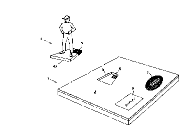
Figure 1 is a perspective view from above of a first
example of the toy;
CA 02273489 1999-06-02
WO 9$/24527 PCT/GB97/03318
6
Figure 2 is a block circuit diagram of the primary
components in the base unit shown in Figure 1;
Figure 3 is a circuit diagram showing the components
within the character of Figure 1;
Figure 4 is a view similar to Figure 1 but of a second
example;
Figure 5 is a block circuit diagram of alternative
primary components in the base unit shown in Figure 1;
Figure 6a is a representation of the frequency
response of the tuned circuit with the character
transmitting data "1";
Figure 6b is a representation of the frequency
response of the tuned circuit with the character
transmitting data "0";
Figure 7a is a representation of the phase change of
oscillation of the tuned circuit compared to that of the
drive signal with the character transmitting data "1"; and,
Figure 7b is a representation of the phase change of
the tuned circuit compared to that of the drive signal with
the character transmitting data "0".
Referring to Figure 1 there is shown a toy having a
base unit 1 in the form of a rectangular housing moulded,
for example, out of plastics. On the upper surface 2 is a
recessed portion 3 trapezoidal in shape to receive a
corresponding trapezoidal base 4a of a piece in the form of
a character 4 e.g. a cartoon or other fictitious character.
The base 4a and recess portion 3 are trapezoidal so that
the base 4a only fits into the recess portion if it is
orientated into the correct position.
Inside the base portion 4a of character 4 is a Tag 5
including a slave unit defined by an electronic circuit
shown in more detail in Figure 3. The Tag 5 is remotely
activatable from energy transmitted thereto and, when
activated, transmits information contained in its memory.
Mounted inside the base unit 2 is a master unit shown
in more detail in Figure 2. The master unit includes a Tag
reader, part of which is shown at 6 in one corner of the
CA 02273489 1999-06-02
WO 98/24527 PCTIGB97/03318
7
recessed portion 3. The Tag reader is connected to a
speake-r 7 and display 8. Batteries (not shown) may be used
to power the reader speaker 7 and display 8, which
batteries may be housed in the base unit 1.
In use of the device of Figure 1, the character 4 is
placed in the recess portion 3 on surface 2 of the base
unit 1. The Tag 5 will thus lie adjacent the part 6 of the
reader 6. The Tag 5 contains information about the
character in for example compressed speech form which is
read by the reader. This information is then displayed
visually on display 8 and/or speech is transmitted through
speaker 7. Such information could include a brief story
about the character or the character's name and what it
does for example.
It is envisaged that the base unit 1 could be -
fabricated and sold with one or more characters. The owner
could then purchase or otherwise acquire different
characters each with the ability to convey different
information.
The components of the Tag reader are shown in more
detail in Figure 2. The reader comprises a microprocessor
20 powered from batteries (not shown) along a power line
21. The microprocessor 20 is connected to the display 8
and the speaker 7 and, although not shown in Figure 1, may
also be connected to a mechanical actuator 22 and an I/0
interface 23 for connection to a remote computer (not
shown). The microprocessor 20 is controlled via software
stored in a memory 24. The microprocessor generates a
clock signal on a line 25 at a rf frequency, e.g. l6MHz,
which is fed to a divider circuit 26 which reduces the
frequency of the signal to 125kHz. This drive or "carrier"
signal is filtered in the filter 27 and amplified by an
amplifier 28 before being fed to a first part 29 of a tuned
circuit. The first part 29 of the tuned circuit includes
a capacitor 30 and a 25 turn inductor 31. In this example,
the capacitor 30 has a value of 39.8nF.
CA 02273489 1999-06-02
WO 98/24527 PCT/GB97/03318
8
The circuit 29 is connected to one input of a phase
comparator 32,- the other input of which receives the
carrier frequency on a line 33. The comparator 32 compares
the phases of the two input signals and generates a binary
output signal whose state corresponds to the determined
phase difference. This signal is fed to a converter
circuit 34, typically in the form of any exclusive-OR gate
which converts the input signal into a pulse width
modulated (PWM) signal which is fed to the microprocessor
IO 20. The microprocessor 20 responds to that signal to
control one or more of the speaker, display, actuator and
I/O interface 7,8,22,23.
Figure 3 illustrates the components within the
character 4 defining the slave unit. The circuit comprises
a second part 40 of the tuned circuit, formed by a 25 turn
inductor 41 and a capacitor 42 having a value in this
example of 28.8nF. The circuit 40 is connected in series
to a further capacitor 43 having a value of 3300pF and in
parallel with a FET 44. The output from the circuit 40 is
connected to a rectifying circuit 45 formed by two diodes
and a capacitor which generates a DC power signal of 5V for
use by the other components within the slave unit. It
should be noted that the slave unit has no internal power
source of its own.
The output from the circuit 40 is also fed to a
divider arrangement 46 of conventional form from which a
clock signal (typically l6Kbits/sec) is derived which is
fed to the clock input 47 of a serial ROM 48 and to one
input of an exclusive-OR gate 49. Data is clocked out of
an output 50 of the serial ROM 48 at half the clock rate
and is fed to the other input of the exclusive-OR gate 49.
The output from the exclusive-OR gate 49 is fed to the gate
of the FET 44.
When the character 4 is brought into proximity with
the recess 3, the part 6 of the Tag reader (corresponding
to part or all of the coil 31) will be brought into
proximity with the coil 41 and the tuned circuit comprising
CA 02273489 1999-06-02
WO 98/24527 PCT/GB97/03318
9
the first and second parts 29,40 will be completed. This
effectively forms an inductive link between the first and
second parts of the tuned circuit.
Thus the application of the drive signal to the first
part 29 of the tuned circuit causes an oscillating magnetic
field to be generated by the coil 31. As long as the first
and second parts 29, 40 of the tuned circuit are
sufficiently close, the magnetic field will induce a
current in the coil 41 of the second part of the tuned
circuit. This current is used to power the processes in
the character 4, as mentioned below, and to generate a
further magnetic field in the coil 41. This further
magnetic field interacts with the field generated by the
coil 31, and as a result, changing the magnetic field
generated by the coil 41 results in a change in the
resonant frequency of the tuned circuit.
However, the magnitude of a magnetic field follows the
inverse square law and decreases proportionally to the
square of the distance from the source. Accordingly, if
the first and second parts 29, 40 of the tuned circuit are
not sufficiently close, the current generated in the coil
41 will be insufficent to power the character circuitry and
the system will not function.
The resonant frequency of the tuned circuit is
slightly different from that of the carrier or drive
signal. Accordingly, the circuit will oscillate at the
frequency of the drive signal with a phase offset to that
of the drive signal such that the comparator 32 will detect
a phase difference between the two. Following conversion
of this phase difference by the converter 34 to a PWM
signal, the state output by the comparator 32 will be
detected by the microprocessor 20. The microprocessor 20
will then momentarily inhibit generation of the carrier
frequency to allow the slave unit within the character to
reset following which the carrier frequency is restarted.
On re-start, power will be coupled from the reader to
the Tag via the tuned circuit and will be rectified by the
CA 02273489 1999-06-02
WO 98/24527 PCT/GB97/03318
rectifying circuit 45 so as to generate a 5v supply. The
alternating signal generated by the tuned circuit will also
be fed to the divider 46 from which the clock is obtained
causing data to be clocked out of the serial ROM 48. Since
5 the data is clocked out of the serial ROM 48 at half the
clock rate, each data bit applied to the exclusive-OR gate
49 will remain applied while the other input of the
exclusive-OR gate 49 receives two clock signals of
complementary value. Thus, the output of the exclusive-OR
10 gate 49 will be two bits either "01" if the data bit on the
input 50 is a "0" or "10" if the data bit on the line 50 is
a "1".
The output from the exclusive-OR gate 49 is fed to the
gate of the FET 44 with a value of "1" turning the gate on
and a value of "0" turning the gate off. When the gate is
turned on, the capacitor 43 will be effectively inserted
into the tuned circuit thus decreasing its resonant
frequency FRS slightly below the frequency of the drive
signal Fd, as shown in Figure 6a. Accordingly, as shown in
Figure 7a, which shows the drive signal Fd and the
oscillation frequency Fo, the tuned circuit will oscillate
at the frequency of the drive signal with a phase lag
compared to that of the drive signal. The comparator 32
detects this phase lag and determines that the data
transferred from the character 4 is a binary "1".
If the output from the exclusive-OR gate 49 is a
binary "0" then the gate of the FET 44 will remain open and
the tuned circuit maintains its normal resonant frequency
FRO , slightly more than that of the drive signal Fd, as
shown in Figure 6b. Accordingly, as shown in Figure 7b,
which shows the drive signal Fd and the oscillation
frequency Fo, the tuned circuit will oscillate at the
frequency of the drive signal with a phase advance compared
to that of the drive signal. The comparator 32 detects
this phase advance and determines that the data transferred
from the character 4 is a binary "0".
CA 02273489 1999-06-02
WO 98/24527 PCT/GB97/03318
11
The oscillation frequency of the tuned circuit will
thus vary in phase relative to the input carrier from the
amplifier 28, depending upon its resonant frequency, the
difference in phase between the two conditions (binary "1"
and binary "0" from the exclusive-OR gate 49) being
typically about 30°.
The difference in phase is detected by the comparator
32, as explained above, and a signal is generated by the
comparator 32 defining the phase difference which is fed to
the converter 34 which in turn generates a pulse width
modulated signal which is fed to the microprocessor 20.
The response of the microprocessor 20 to the signal
from the converter 34 will depend upon the type of
information being transmitted. Typically, the serial ROM
48 will contain header information which is initially
downloaded to the microprocessor 20 and this will define
the type of data which is to follow, for example programme
data, display data, audio data or the like. The
microprocessor 20 responds to the header information by
processing the following data as appropriate.
If the following data defines a programme then it will
be fed, if necessary after further modification by the
microprocessor 20, to the memory 24 for storage, following
which the microprocessor 20 will carry out the stored
programme.
If the data defines audio information, for example it
may comprise compressed audio data, the microprocessor 20
will decompress the data and then apply appropriate control
signals to the speaker 7 which will generate an audio
message.
If the data defines display information, typically in
compressed form, the microprocessor 20 will decompress that
data and convert it into suitable control signals (for
example R, G, B signals) which are then applied to the
display 8 which typically comprises a monitor.
If the data comprises mechanical movement data, the
microprocessor 20 will generate from it suitable control
CA 02273489 1999-06-02
WO 98/24527 PCT/GB97/03318
12
signals which are fed to the actuator 22. The actuator 22
may be. connected to an arm or signal or the like.
In addition the data may be at least temporarily
stored.
Instead of the pieces being in the form of characters
or models, they could simply be cards or other objects
incorporating slave units. In such an instance the
recessed portion 3 on surface 2 might take a different form
to accommodate the cards. It is pointed out that it is not
essential for the surface of the base unit 1 to have a
recess portion to receive the pieces. Thus, as shown in
Figure 4, the base unit 2A has no recess, the Tag Reader
part 6A being positioned under the surface of the base
unit. Also it is not essential for the reader to be
adjacent and in close proximity to the Tag in a piece in
order for the reader to interface with the Tag. The reader
and Tag could be distanced apart, for example by up to 2cm.
In a further application, the game could involve a
ball and goal, a slave unit incorporated in the ball and a
master unit in or adjacent to the goal. When the ball
passes into the goal, data is transmitted to the master
unit which will thus detect a goal scored and optionally
generate relevant information obtained from the slave unit
store.
The master unit could also include its own data which
is used to control one or more of the output devices either
separately from or with data from the slave unit.
It will be realised that any suitable tuned circuit
that allows inductive coupling between the master unit and
the character 4 could be used. An alternative example of
such a circuit is shown in Figure 5. This apparatus is
similar to that of Figure 2, with the first part 29 of the
tuned circuit replaced by an alternative first part 129 of
a tuned circuit. The first part 129 comprises a 25 turn
inductor 131 coupled to the comparator 32 and the output of
the amplifier 28. A capacitor 130 is coupled from the
connection between the inductor 131 and the comparator 32
CA 02273489 1999-06-02
WO 98124527 . PCT/GB97/03318
13
to ground, for optimising the resonant frequency of the
first part 129 of the tuned circuit.