Note: Descriptions are shown in the official language in which they were submitted.
CA 02273858 1999-06-O1
WO 98126631 - PCTIDK98/00521
POWER SUPPLY FOR MICROPHONE
The invention concerns a circuit for the amplification,
analog signal processing and A/D conversion of signals from
a microphone as defined in the preamble to claim 1.
It is known within microphone and audio technology to
integrate D/A conversion and microphone amplification in
one unit, so that the sampling point is moved as close as
possible to the microphone, and herewith reduce signal
distortion, noise and hum which can arise with long signal
paths. To reduce noise pulses, it is known from patent
application GB-A-2 293 740 to build A/D converters and
microphone power supplies on the same circuit board, where
the microphone power supply works with pulse modulation at
a frequency which is derived from the sampling frequency in
the A/D converter. This patent application forms the basis
for the two-part form of claim 1.
Where a wide range of portable products within
telecommunication, video and audiometrics are concerned, as
well as hearing aids and other micro-electronics, the
weight and the physical dimensions of the equipment play an
important role for the equipment's fields of application
and marketability.
The power consumption belongs typically among the important
factors which, together with the relevant battery
technology, are determinative for precisely the weight and
the physical dimensions of the portable equipment.
Therefore, in many connections it is decisive that attempts
are made to reduce the power consumption as much as
possible.
With active microphones, such as electret microphones,
these are normally supplied with a constant current which
CA 02273858 1999-06-O1
WO 98J26631 - PCT/DK96J00521
2
is in the magnitude of 100 - 600 ~A. For the above-
rnentioned applications, this constitutes a high current
consumption. It is therefore a principle object of the
present invention to reduce the current consumption.
This is achieved with the invention as defined in claim 1.
According to the invention as defined in claims 2 - 4, a
strongly reduced current consumption is achieved, in that
the microphone coupling is provided with current pulses of
such a short duration that the microphone current reaches a
usable value. The current consumption in such a coupling is
typically only 0.01 - 0.03 uA per duty cycle.
According to the invention as defined in claim 5, a
particularly advantageous coupling is achieved, in that the
coupling together of the microphone and amplifier in one
unit makes a high signal/noise ratio possible.
With reference to the figures, the invention will be
described in more detail in the following, in that
fig. 1 shows a principle diagram of the circuit,
fig. 2 shows an example embodiment of the invention, and
fig. 3 shows the signal sequences for the circuit
according to the invention.
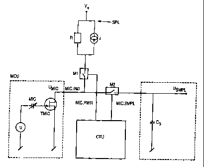
In the principle diagram, fig. 1, is shown an electret
microphone which, for example, can have an upper limit
frequency of around 15 kHz. This upper limit frequency can
also lie closer to the maximum limit frequency of the
audible range if a microphone of high quality is used. The
microphone can be protected by a thin protective net, such
as a thin layer of foam material which, however, will
CA 02273858 1999-06-O1
WO 98126631 - PCTIDK96/00521
3
reduce the upper limit frequency of the microphone
membrane.
The membrane on an electret microphone comprises a variable
capacitor which changes depending on the acoustic signal to
which the microphone is exposed. In the manufacture of the
electret microphone, the membrane is provided with a
permanent charge which can remain unchanged for several
years. The equivalent diagram for an electret microphone
can thus be considered as a battery in series with a
variable capacitor.
In the principle diagram, fig. 1, a microphone unit, MCU,
comprises such an electret microphone and a transistor,
TMIC, which is placed physically close to the membrane arid
connected to the membrane's terminals. The transistor TMIC
can with advantage be a J-FET transistor because of the
ideal infinitely high input impedance of this type of
transistor. Small signals from signal sources with high
output impedance can hereby be amplified for further signal
processing.
For the registration of the membrane movement, according to
the invention there is disclosed a voltage generator and
possibly a current generator for supplying the transistor
TMIC in the microphone and the subsequent signal processing
with electrical energy. Fig. 1 shows a voltage generator
and a current generator which are equivalent to a non-ideal
impedance connected in parallel with a constant current
generator. This power supply has the designation SPL.
The object of the above-mentioned generators is to provide
the transistor TMIC with a constant operating current which
is selected in accordance with the optimum working
specifications of the transistor.
CA 02273858 1999-06-O1
WO 98/26631 - PCT/DK96i00521
4
A membrane deflection for a given time will give rise to a
certain voltage across the microphone membrane's terminals,
which will result in a current which is proportional to the
membrane deflection through the transistor TMIC.
The constant working current is thus modulated by the
acoustically-derived signal, so the current through TMIC
varies around the constant working current. It is this
constant working current which is desired to be reduced by
the invention.
For reasons of cost, the current generator in the above-
mentioned coupling can be dispended with. However, this
alternative will result in a lower signal/noise ratio, the
reason being that the transistor does not work under ideal
conditions.
According to the invention, the transistor TMIC is provided
with current across an electric switch M1 which is
controlled by a digital control circuit CTU via the signal
MIC.PWR. This switch, M1, is opened and closed at periodic
intervals of T and is active for the time t1.
The voltage Umic from the microphone supplies a sampling
capacitor C5 via the electric switch M2, which is active
for the time t2 and is controlled by the signal MIC.SMPL
from the control unit CTU. This signal is converted to
digital values by a subsequent sampling circuit (not shown)
which, synchronously with M1 and M2, operates at the
sampling frequency 1/T.
The sampling frequency or the Nyquist frequency can be
selected in the normal manner to be at least double the
desired upper limit frequency of the audio signal. Sampling
can also be effected in the conventional manner with over-
sampling in order to reduce negative effects of filtration
CA 02273858 1999-06-O1
WO 98/26631 - PCTlDK96~00521
of the higher harmonic contributions from the sampling
process.
It is also possible for the sampling process to be effected
5 by a circuit working analogically.
The time sequence of the signals MIC.PWR and MIC.SMPL is
shown in fig. 3:
The time t1, where M1 conducts current to the transistor
TMIC, is considerably shorter than the time period T, and
is selected to be of sufficient length for Umic to reach a
usable value. The microphone amplifier is thus provided
with relatively short pulses seen in comparison with the
sampling time T.
Within the time t1, the output signal from the microphone
is more or less constant, seen in relation to the
variations within the time T, and a certain value higher or
lower than at the last sample. This signal change will now
give rise to a change in the current through the transistor
TMIC.
Since in practice the microphone/transistor coupling
MIC/TMIC contains parasite capacitances across the
terminals, the current through the transistor can not rise
more quickly than that speed at which these capacitances
can be charged and discharged. Umic thus follows a charging
or discharging sequence which converges asymptotically
towards a value which is proportional to the change of the
given membrane deflection in relation to the last sample.
A typical sequence of Umic 1s thus shown in fig. 3.
The magnitude of the signal Umic~ indicated by the stippled
lines in fig. 3, thus depends on the amplitude of the
CA 02273858 1999-06-O1
WO 98/26631 - PCTIDK96~00521
6
audio signal for a given time.
The sampling circuit reads Umic as late as possible within
the time t1, the reason being that Umic has the best
signal/noise ratio at the end of t1. Usmpl zs thus active
in a window with the duration t2 seen from the rear flank
of the active part of the supply pulse t/ controlled by Ml.
The time t2 is shorter than t1 and, depending on the speed
at which C5 is charged, can be selected to be considerably
shorter than t1.
Umic can be considered as being more or less constant
within the time t2, and the charging of the sampling
capacitor C5 in the time t2 can be approximated by an RC
circuit in which R can vary from 500 ohms - 5 Kohms, since
the resistance of the electric switch M2 is insignificant.
Typical values for the time constant which applies during
t2 will then be 0.05 - 0.5 us when C5 is of 100 pF.
The sampling capacitor C5 will thus be charged or
discharged at the above-mentioned time constant which
applies during t2 from the previous sample value towards a
level which asymptotically approaches the voltage across
the microphone membrane at a given time. This voltage,
IJsmpl' is seen in fig. 3.
How short t1 can be set in practice will depend on how low
a signal/noise ratio can be accepted for Umic' which among
other things must be selected in accordance with the
parasite capacitances arising in the microphone transistor
TMIC and with the accuracy of the sampling process and the
use in general. It has proved in practice that a
commencement of the sampling pulse (M2) already at t1 - t2
corresponding to the double time constant (2 RC gives exp(-
2RC/RC)=0.86) provides usable values. Typical values of t1
can lie at 0.2 - 3.0 us.
CA 02273858 1999-06-O1
WO 98126631 - PCT/DK96>00521
7
If, for example, it is desired to transfer an audio signal
of up to 20 kHz, and a sampling frequency of 44 kHz is used
( T - 23 us ) , it is seen that the low values of t1 and t2
stated above will give rise to a considerable saving in
current.
Speech signals can be transferred with acceptable results
at a sampling frequency of e.g. 10 kHz (T = 100 us), and in
this case it is evident that the saving in current is even
greater for the pulsed microphone circuit.
In fig. 2 is seen an example embodiment where the current
generator in fig. 1 is configured with an operational
amplifier OP1 which feeds the signal Usmpl back through an
electric switch M1 to the base of a transistor T1, which in
turn supplies a microphone unit MCU (not shown in fig. 2),
which couples current to the terminal MIC.IND.
The operational amplifier is connected to the resistors R4,
R5 and R6 and the capacitor C3, which removes possible
noise from OP1.
The transistor T1 is biased by the resistor network R1 and
R2.
The output from the microphone unit can be damped via a
capacitor as shown by C1 in order to avoid possible
frequency contributions over the half sampling frequency
being conducted further to the sampling circuit.
The signal from the microphone Umic is fed across the
electric switch M2, which in practice is connected to small
parasite capacitances, forward to the sampling capacitor
C5, across which there is coupled a subsequent A/D
converter circuit~with possible limiter circuit.
CA 02273858 1999-06-O1
WO 98/26b31 - PCT/DK96100521
8
M1 and M2 are controlled via the signals Micpwr and Micsmpl
by a control circuit CTU to operate as described above and
synchronously with the sampling circuit SMPL.
The object of the coupling in fig. 2 is to adjust or to
adapt the current through the microphone, so that a
suitable average value for the voltage across C5 is
obtained. The voltage across C5 is controlled in accordance
with the adjustable level V , so that TMIC in the
bias
microphone works at an optimized operation point.
The present invention is naturally not limited only to
electret microphones as described in the example
embodiment. The invention can be used with advantage for
other types of active microphones, such as capacitor
microphones with external power source and piezo-sensitive
semi-conductor microphones. Similarly, other types of semi
conductor components can be used instead of J-FET
transistors.
A limiter circuit can be inserted in the signal path before
the sampling circuit. According to the invention, these
circuit elements can similarly operate in a sampled manner
and hereby further reduce the current consumption.
Component list for the circuit in fig. 2:
R1 470 ohms
R2 330 ohms
R4 15 Kohms
R5 1 Megohm
R6 47 Kohms
C1 10 pF
c3 to uF
CA 02273858 1999-06-O1
WO 98/26631 - PCT/DK96f00521
9
C5 100 pF
T1 BSR 20 A - BF 411
M1 IC 101 A - HC 4066
M2 IC 101 B - HC 4066
Opl IC 102 B - HC 4066