Note: Descriptions are shown in the official language in which they were submitted.
CA 02273949 1999-06-02
SPECIFICATION
Circuit Chip Mounted Card and Circuit Chip Module
Technical Field
The present invention relates to circuit chip mounted cards and
circuit chip modules, and more particularly to a circuit chip mounted card
and a circuit chip module with increased reliability, reduced manufacturing
cost and the like.
Background Art
Non-contact type IC cards are used for the gate of the ski lift, the
gate at the station, automatic sorting of parcels and the like. A
conventional non-contact type IC card is exemplified in Fig. 12. An IC
card 2 shown in Fig. 12 is an IC card of a single coil type, and includes a
coil 4, capacitors C 1 and C2 and an IC chip 8.
Capacitors C1 and C2 and IC chip 8 are included in a film substrate
formed of synthetic resin. The substrate including capacitors C1 and C2
and IC chip 8 are referred to as a tab (tab: tape automated bonding) 10.
Fig. 13A is a cross sectional view showing IC card 2. A core member
12 of synthetic resin is interposed between su~~face layer matexzals 14 and
1G. Tab 10 including capacitors C1 and C2 and IC chip 8 is fixed to
surface layer material 14 which is exposed to a cavity 18 in core member 12.
A connection of tab 10 and IC chip 8 is covered with a sealing material 9 of
epoxy resin or the like.
Coil 4 is arranged between surface layer material 14 and core
member 12. A wire 20 connects coil 4 and tab 10.
Fig. 13B is a circuit diagram showing IC card 2. IC card 2 receives
an electromagnetic wave transmitted from a reader/writer (reading/writing
apparatus, not shown) by a resonance circuit 22 formed of coil 4 and
capacitor C 1 as a power source. It is noted that capacitor C2 is used for
smoothing power.
In addition, a control portion (not shown) provided in IC chip 8
decodes information transmitted by the electromagnetic wave for response.
-1-
CA 02273949 1999-06-02
The response is performed by changing an impedance of resonance circuit
22. The reader/writer obtains a content of the response by detecting a
change in an impedance (impedance reflection) of its own resonance circuit
(not shown) due to the change in the impedance of resonance circuit 22 on
the side of IC card 2.
Thus, the use of IC card 2 allows data communication in a non-
contact state without a power supply source in the card.
However, the above described conventional IC card suffers from the
following problem.
In IC card 2, coil 4 and tab 10 must be connected by wire 20. On the
other hand, IC card 2 is often put in a wallet or a pocket of a trouser, where
it is subjected to considerable bending, twisting and pressing forces.
However, a thickness t of IC card 2 shown in Fig. 13A is standard and not
so thick. Thus, it is not provided with a significant rigidity against such
bending, twisting and pressing forces. Therefore, if IC card 2 is subjected
to a significant bending force or the like, a consider able deflection is
caused.
Such deflection may result in a breakage of wire 20 or disconnection of wire
and coil 4 or tab 10. In addition, wire 20 may not be well connected to
coil 4 or tab 10.
20 Further, to ensure a space for coil 4, tab 10 must restrictively be
positioned. Thus, in some cases, tab 10 must be provided in a position
where a significant deflection is caused. This may result in significant
deformation of IC chip 8. Accordingly, IC chip 8 is cracked and does not
well function as an IC card.
As described above, the conventional IC card is difficult to handle
and lacks in reliability.
Moreover, as coil 4 and tab 10 must be connected by wire 20,
complicated assembly is involved, thereby increasing a manufacturing cost.
In addition, provision of capacitors C 1 and C2 and the like in tab 10 further
increases the manufactuxzng cost.
Disclosure of the Invention
An object of the present invention is to provide a circuit chip
mounted card with high reliability and low manufacturing cost by
-2-
CA 02273949 1999-06-02
overcoming the aforementioned problem related to the conventional card.
According to one aspect, the circuit chip mounted card of the present
invention which achieves the above object includes: an antenna for
communication utilizing an electromagnetic wave; a processing portion
performing a process for communication; a first circuit chip including at
least a portion of a processing portion and having a terminal; and a second
circuit chip including the antenna and the remaining portion of the
processing portion and having a terminal, and is characterized in that the
terminals are electrically connected by stacking the first and second circuit
chips in a direction of thickness of the card.
According to the present invention, such structure eliminates the
need for arranging the interconnection outside the circuit chip because a
function of communication is achieved simply by stacking two circuit chips
including the functions of the processing portion and antenna. Thus,
insufficient connection caused by external arrangement of the
interconnection is avoided. Further, even if the deflection is repeatedly
caused for the card, breakage of the external arrangement of the
interconnection or accidental disconnection would be avoided.
In addition, as the antenna is included in the second circuit chip
which is in turn stacked on the first circuit chip, the positional restriction
of
the circuit chip to ensure a space for the antenna is eliminated. Thus, the
stacked circuit chips with a small area when viewed from above is provided
in an arbitrary position where a significant deflection would not be caused.
As a r esult, even when a significant force is applied to the card, the
circuit
chips would not significantly be deformed.
Further, as the interconnection needs not be externally arranged,
assembly is extremely facilitated. Thus, reduction in the manufacturing
cost is achieved. In addition, as the capacitor is also included in the
circuit
chip, the work for mounting the capacitor is not necessary. This results in
further reduction in the manufacturing cost. Therefore, the circuit chip
mounted card with high reliability and low manufacturing cost is achieved.
The circuit chip mounted card according to the present invention
having the above described structure is obtained preferably by providing
-3-
CA 02273949 1999-06-02
the terminal for the first circuit chip on the side of the second circuit
chip,
providing the terminal for the second circuit chip on the side of the second
circuit chip such that it is opposite to the terminal for the first circuit
chip,
and directly connecting the first and second circuit chips in a stack.
Such structure allows two circuit chips to be readily connected to
form a module using a conventional technique for connecting the terminals.
Thus, further reduction in the manufacturing cost is achieved as
workability during manufacture increases.
According to another aspect, a circuit chip mounted card of the
present invention provided with an antenna for communication utilizing an
electromagnetic wave and a processing portion performing a process for
communication includes: a first base material; a second base material
arranged in a direction of thickness of the card spaced from the first base
material with a prescribed distance; a core member layer interposed
between the first and second base materials; and a circuit chip module
arranged in the core member layer. The circuit chip mounted card is
characterized in that it is a composition of a first circuit chip including at
least a portion of the processing portion and having a terminal and a
second circuit chip including the antenna and the remaining portion of the
processing portion and having a terminal arranged opposite to the terminal
of the first circuit chip which are stacked and connected in a direction of
thickness of the card through an anisotropic conductor to electrically
connect the terminals.
According to the present invention, such structure allows two circuit
chips to be securely connected with the anisotropic conductor interposed.
In most cases, an opening is provided in the circuit chip for external
arrangement of the interconnection before the circuit chip is mounted in
the card, which opening leads to an interconnection layer of aluminum or
the like through a protection film on a surface. Thus, the aluminum of the
interconnection layer may suffer from corrosion during a period from the
manufacture of the circuit chip to mounting in the card and due to secular
change after assembly. In the circuit chip mounted card according to the
present invention, the first and second circuit chips can be connected
-4-
CA 02273949 1999-06-02
through the anisotropic conductor after manufacture, as external
arrangement of the interconnection is not necessary when they are
mounted in the card. In other words, corrosion of the aluminum of the
interconnection layer or the like is reduced as the first and second circuit
chips are closely connected through the anisotropic conductor.
In a preferred embodiment of the circuit chip mounted card
according to the present invention, a reinforcing member including a frame
which is arranged to surround the first and second circuit chips in a
direction of the face of the chip is provided in the card.
Such structure effectively increases rigidity of the card in vicinity of
the circuit chip while ensuring a space for the stacked circuit chips. Thus,
even if significant bending, twisting and pressing forces are applied to the
card, the stacked circuit chips would not signih.cantly be deformed. In
other words, the circuit chip mounted card is provided with increased
reliability.
According to one aspect, a circuit chip module of the present
invention forming a card with a circuit including an antenna for
communication utilizing an electromagnetic wave and a processing portion
performing a process for communication includes: a first circuit chip
including at least a portion of the processing portion and a terminal; and a
second circuit chip including the antenna and the remaining portion of the
processing portion and having a terminal, and is characterized in that the
first and second circuit chips are stacked in a direction of thickness of the
card to electrically connect the terminals.
Such structure of the circuit chip module according to the present
invention enables a communication function to be performed only by a
small circuit chip module. Thus, elements in the card can more freely be
arranged. In addition, as a preliminary formed single module is merely
involved for assembly, the manufacturing cost is further reduced with
increased workability.
In a preferred embodiment of the circuit chip module according to the
present invention, a resonance frequency of a resonance circuit including a
capacitor provided inside the circuit chip and a coil for the antenna can be
-5-
CA 02273949 1999-06-02
adjusted.
Such structure allows the capacitance or inductance of the resonance
circuit to be adjusted after the capacitor and coil are formed in the circuit
chip. Thus, the resonance frequency can be adjusted after formation of
circuit elements though these circuit elements of the resonance circuit are
all formed in the circuit chip.
More specifically, the circuit chip mounted card is provided with high
reliability as the resonance frequency can be maintained at a prescribed
level to some extent even if there is a variation in manufacturing conditions.
Further, since a circuit chip corresponding to various resonance frequencies
is obtained without changing a mask pattern for forming the circuit
elements in a manufacturing process of the circuit chip, the manufacturing
cost is not increased.
According to another aspect, a circuit chip module of the present
invention is a composition of circuit chips including stacked first and
second circuit chips, and characterized in that at least one of the first and
second circuit chips is provided with a detour interconnection which
electrically connects two terminals of the above mentioned one circuit chip
and the detour interconnection electrically connects two terminals of the
other circuit chip respectively connected to the two terminals.
With such structure, the circuit chip module according to the present
invention can only perform an essential function when two circuit chips are
connected. Thus, even when the circuit chip module is divided into two
circuit chips, it is difficult to analyze the function by each terminal. A
plurality of detour interconnections would further make it difficult to
analyze the function. In other words, the circuit chip module with high
security is achieved.
Brief Description of the Drawings
Fig. 1 is a view showing an overall appearance of a non-contact type
IC card 70 according to one embodiment of the present invention.
Fig. 2 is a cross sectional view taken along the line II-II in Fig. 1.
Fig. 3A is a front view showing an IC chip module 74, and Fig. 3B is
a view showing elements of IC chip module 74 before they are connected
-6-
CA 02273949 1999-06-02
together.
Fig. 4 is a schematic diagram showing an IC chip 76 shown in Fig.
3B when viewed from above (from the side of a bump 82).
Fig. 5 is a schematic diagram showing an IC chip 78 shown in Fig.
3B when viewed from below (from the side of a bump F4).
Fig. 6 is a diagram shown in conjunction with a detour
interconnection and dummy bump.
Fig. 7 is a cross sectional view showing a non-contact type IC card 30
according to another embodiment of the present invention.
Fig. 8 is a cross sectional view showing a non-contact type IC card 50
according to still another embodiment of the present invention.
Fig. 9 is a cross sectional view showing a non-contact type IC card
170 according to still another embodiment of the present invention.
Fig. 10 is a diagram showing a resonance circuit 150 of an IC chip
module according to still another embodiment of the present invention.
Fig. 11 is a diagram showing a resonance circuit 160 of an IC chip
module according to still another embodiment of the present invention.
Fig. 12 is a view exemplifying a conventional non-contact type IC
card.
Fig. 13A is a cross sectional view taken along the line XIIIA-XIIIA in
Fig. 12, and Fig. 13B is a circuit diagralri of an IC card 2.
Best Modes for Carrying Out the Invention
Fig. 1 is a view showing an overall appearance of non-contact type IC
card 70 as a circuit mounted card according to one embodiment of the
present invention. IC card 70 is a single coil type IC card which can be
used for the gate of the ski lift, the gate at the station and automatic
sorting of parcels and the like.
Fig. 2 is a cross sectional view taken along the line II-II in Fig. 1.
IC car d 70 has a structure having a surface layer material 32 of a first base
material, a core member 34 forming a core member layer and a suWace
layer material 3G of a second base material, which are stacked in this order.
Synthetic resin such as vinyl chlo~~ide, PET (polyethylene terephthalate) or
the like is used for surface layer materials 32 and 3G. Core member 34
_7_
CA 02273949 1999-06-02
includes synthetic resin.
A cavity 72 is provided in the layer of core member 34. In cavity 72,
an IC chip module 74 is fixed as a circuit chip module in contact with
surface layer material 32.
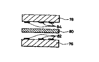
Fig. 3A is a front view of IC chip module 74. IC chip module 74 is a
composition including an IC chip 76 of a first circuit chip and an IC chip 78
of a second circuit chip which are stacked in a direction of thickness (see
Fig. 2) of IC card 70 through an anisotropic conductor 80.
Fig. 3B shows elements of IC chip module 74 before they are
connected together. IC chip 76 is provided on its top with a plurality of
bumps 82 for terminals. IC chip 78 is provided on its bottom a plurality of
bumps 84 for terminals. Bumps 82 and 84 are arranged in mutually
opposite positions.
Anisotropic conductor 80 is a conductor having a conductivity only in
one direction and provided with adhesion. As the anisotropic conductor,
anisolum (Hitachi Chemical Co., Ltd.), which is a thermosetting adhesive,
is used. Such anisotropic conductor 80 enables IC chips 7G and 78 to be
firmly adhered. Adhesion of IC chips 76 and 78 using anisotropic
conductor 80 allows bumps 82 and 84 provided in mutually opposite
positions to be electrically connected. Thus) IC chip module 74 is formed.
Fig. 4 is a schematic diagram showing IC chip 7G when viewed from
above (from the side of bumps 82). IC chip 7G is provided with a non-
volatile memory (not shown) and a modulating/demodulating circuit (not
shown) which are part of the processing portion and the like.
Fig. 5 is a schematic diagram showing IC chip 78 when viewed from
below (from the side of bumps 84). IC chip 78 is provided with a coil 44 of
an antenna, capacitors C1 and C2 which are the remaining portion of the
processing portion and the like. A metal interconnection layer is
configured in a loop like shape to form coil 44. At least one of capacitors
C 1 and C2 includes a ferroelecti~ic substance. In addition, coil 44 and
capacitor C 1 form a resonance circuit. Capacitor C2 is used for smoothing
a power supply.
Such structure enables a communication function to be achieved
_g_
CA 02273949 1999-06-02
simply by stacking IC chips 7G and 78 provided with functions of the
processing portion and the antenna, so that the interconnection needs not
be arranged outside IC chips 76 and 78. In addition, even if deflection is
repeatedly caused for IC card 70, breakage of the external interconnection
or accidental disconnection would not happen.
Further, a position in which the IC chip is arranged is not restricted
to ensure a space for a coil because coil 44 is included in IC chip 78 which
is
stacked on IC chip 7G. Thus, IC chips 76 and 78 with a small area when
viewed from above can be arranged in an arbitrary position where a
significant deflection would not be caused. As a result, even if a
significant force is applied to IC card 70, stacked IC chips 7G and 78 would
not significantly be deformed.
Since the connecting operation of the external interconnection is
eliminated, assembly operation would be extremely facilitated. Thus,
reduction in the manufacturing cost is achieved. Further, as capacitors C1
and C2 are also included in IC chip 78, operation for mounting these
capacitors C1 and C2 is not necessary. As a result, further reduction in
the manufacturing cost is achieved.
A small IC chip module 74 can perform the communication function.
Thus, the elements in IC card 70 are more freely arranged. Preliminary
formed single IC chip module 74 needs only be handled during assembly, so
that further reduction in the manufacturing cost is achieved with increased
workability.
Next, the detour interconnection) dummy bump and dummy
interconnection used in IC chip module 74 will be descxzbed. Fig. G is a
diagram shown in conjunction with the dummy bump and detour
interconnection.
For IC chips 76 and 78, bumps 8Ga to 8Ge and 88a to 88c shown in
Fig. G are provided in addition to bumps 82 and 84 shown in Fig. 4 and 5.
Further, interconnections 90a, 90b and 92 are provided. The
interconnection shown in Fig. G corresponds to the detour interconnection.
Bumps 86e and 88c are dummy bumps.
Bumps 8Ga and 8Gb provided for IC chip 76 are connected by an
_g_
CA 02273949 1999-06-02
interconnection 90a provided for IC chip 76. Bumps 8Gc and 86d are
connected by an interconnection 90b provided inside IC chip 7G. On the
other hand, bumps 88a and 88b provided for IC chip 78 are connected by an
interconnection 92 provided inside IC chip r8.
Bump 8Gb provided for IC chip 76 and bump 8Ga provided for IC chip
78 are arranged in opposite positions. Similarly, bump 8Gc provided for IC
chip 7G and bump 86a provided for IC chip 78 are arranged in opposite
positions.
Thus, when IC chips 7G and 78 are connected through anisotropic
conductor 80 (see Fig. 3B), bump 86a provided for IC chip 7G is connected to
bump 8Gd through interconnection 90a, bump 86b, bump 88a,
interconnection 92, bump 88b bump 8Gc and interconnection 90b.
With such structure, IC card 70 would not perform an essential
function unless two IC chips 7G and 78 are connected. Thus, even if IC
chip module 74 is to be divided into two IC chips) it is difficult to analyze
the function by each terminal.
Although bump SGe provided for IC chip 76 and bump 88c provided
for IC chip 78 are arranged in opposite positions, they are dummy bumps
which are not electrically connected to any other element. Further, the
interconnection (not shown) which is not connected to any element other
than bumps may be provided. This is called a dummy interconnection.
Provision of a plurality of such detour interconnection, dummy
bumps and dummy interconnections makes it more difficult to analyze the
function. In other words, an IC chip module with high security is achieved.
In addition, an IC card with high security is achieved by inclusion of such
IC chip module 74.
It is noted that thicknesses of surface layer materials 32 and 3G are
both O.lmm and an overall thickness of IC card 70 is 0.768mm. Each of IC
chips 76 and 78 is square in shape having a side of 3mm, an internal
thickness of the IC chip is 0.2mm, and thicknesses of bumps 82 and 84 are
both 0.1 lmm. A thickness of IC chip module 74 after connection is about
0.55mm. It is noted that the present invention is not limited to these
dimensions and materials.
-10-
CA 02273949 1999-06-02
An operation of IC card 70 is similar to that of conventional IC card 2.
In other words, an electromagnetic wave transmitted from a reader/writer
(writing/reading apparatus, not shown) is received by a resonance circuit
(not shown) formed of coil 44 and capacitor C1 included in IC chip 78 as a
power source. The received power is smoothed by capacitor C2.
The information transmitted by the electromagnetic wave is decoded
by a control portion (not shown) provided in IC chip 76 for response. The
response is performed by changing an impedance of the resonance circuit.
The reader/writer obtains a content of the response by detecting a change
in an impedance of its own resonance circuit (not shown) due to the change
in the impedance of the resonance circuit of IC card 77.
Thus, information is transmitted and received in a non-contact state
without providing a power supply source in the card.
It is noted that although IC chips 76 and 78 are connected together
in a stack with anisotropic conductor 80 interposed in the above
embodiment, IC chips 76 and 78 may be directly connected without
anisotropic conductor 80 interposed. In this case) for example, one of
bumps 82 and 84 may be formed of gold (Au) and the other of tin (Su), so
that they are connected by utilizing eutectic. Thus, two IC chips 76 and 78
can readily be connected to form a module using a conventional technique
of connecting terminals.
In addition, in the above described embodiment, although at least
one of capacitors C 1 and C2 is formed of a ferroelectric substance, all of
the
capacitors may be formed of general dielectric capacitors.
Although an antenna included in IC chip 78 corresponds to coil 44
formed on metal interconnection layer 6, the antenna is not limited to such
configuration. Further, although capacitors C1 and C2 are both formed in
IC chip i8, the coil and capacitor may be formed in different IC chips.
Fig. 7 is a cross sectional view showing a non-contact type IC card 30
as a circuit chip mounted card according to another embodiment of the
present invention. The appearance of IC card 30 is almost the same as
that of IC card 70. Further, IC chip module 74 looks almost the same as
that in the case of IC card 70. Thus, the operation of IC card 30 is similar
-11-
CA 02273949 1999-06-02
to that of IC card 70.
As shown in Fig. 7, IC card 30 includes a surface layer material 32 of
a first base material, a core member 34 and a surface layer material 36 of a
second base material, which are stacked in this order. Synthetic resin
such as vinyl chloxzde, PET (polyethylene terephthalate) or the like is used.
In addition, core member 34 is formed of synthetic resin.
A ceramic frame 38 is provided in the layer of core member 34.
Ceramic frame 38 includes ceramic in a cylindrical shape. Ceramic frame
38 corresponds to a frame of a reinforcing member. In other words, the
reinforcing member includes only a frame in the present embodiment.
Internal portion 38a of ceramic frame 38 is a cavity. An elastic
material 40 is provided as a shock absorbing material at a lower end of
internal portion 38a of ceramic frame 38 in contact with surface layer
material 32. Silicon rubber provided with adhesion is used as elastic
material 40. IC chip module 74 as a circuit chip module is supported by
elastic material 40.
As the reinforcing member includes ceramic, high rigidity is ensured.
Thus, provision of ceramic frame 38 in the layer formed of core member 34
greatly increases bending, twisting and pressing rigidity of IC card 30 in
vicinity of ceramic frame 38.
As a result, even if a significant bending, twisting and pressing force
or the like is applied to IC card 30, IC chip module 74 provided in internal
portion 38a of ceramic frame 38 would not significantly be deformed. Thus,
even if a bending, twisting, pressing force or the like is applied, it is
unlikely that IC chip module 74 would be damaged. In other words, IC
card 30 is provided with higher reliability.
Further, since IC chip module 74 is fixed with elastic material 40
interposed, even when a shock is applied to IC card 30, it is not directly
transferred to IC chip module 74. Thus, damage of IC chip module 74 due
to the shock is reduced.
It is noted that thicknesses of surface layer materials 32 and 36 are
both O.lmm and an overall thickness of IC card 30 is 0.7G8mm in the
present embodiment. In addition, IC chip module 74 is a square having a
-12-
CA 02273949 1999-06-02
side of 3mm. It is noted that a thickness of IC chip module 74 is set to
about 0.4mm unlike the above described embodiment.
A thickness of elastic material 40 is 0.118mm. A height of ceramic
frame 38 is 0.568mm. An inner diameter of ceramic frame 38 is set such
that a clearance with respect to the mounted IC chip module 74 is about
0.2mm to 0.3mm. Further, an outer diameter of ceramic frame 38 is about
23mm. It is noted that the present invention is not limited to these
dimensions and materials.
In the present embodiment, IC chip module 74 is fixed to surface
layer material 32 with elastic material 40 as shown in Fig. 7. However, IC
chip module 74 may directly be fixed to surface layer material 32 without
elastic material 40 interposed.
Fig. 8 is a cross sectional view showing a non-contact type IC card 50
as a circuit chip mounted card according to still another embodiment of the
present invention. An overall structure of IC card 50 is similar to that of
IC card 30.
In IC card 50, however, ceramic frame 52 is different from ceramic
frame 38 of IC card 30 in shape as shown in Fig. 8. More specifically,
ceramic frame 52 is different from ceramic frame 38 formed of only a frame
in a cylindrical shape in that it includes a cylindrical portion 52a of a
frame
and a plate like bottom portion 52b integrated with the lower end of
cylindrical portion 52a.
Further, as shown in Fig. 8, IC chip module 74 is structured to be
directly fixed to bottom portion 52b of a recessed space 52c defined by
cylindrical portion 52a and bottom portion 52b of ceramic frame 52.
Thus, as bottom portion 52b is integrated with the lower end of
cylincliical portion 52a, ceramic frame 52 is provided with higher rigidity.
Thus, even when cer amic frame 52 is incr eased in size in face directions (X
and Y directions in Fig. 1) to some extent, desired rigidity is ensured.
Accordingly, the dimension of IC chip module 74 is increased. Therefore, a
dimension of coil 44 included in IC chip module 74 is further increased.
As shown in Fig. 8, frame module 54 is formed with ceramic frame 52
and IC chip module 74 fixed to ceramic frame 52. Such module enables
-13-
CA 02273949 1999-06-02
increase in workability during manufacture and reduction in the
manufacturing cost.
Although IC chip module 74 is structured to be directly fixed to
bottom portion 52b of ceramic frame 52 in the present embodiment, elastic
material 40 as shown in Fig. 7 may be interposed between IC chip module
74 and bottom portion 52b of ceramic frame 52. Such structure reduces
the shock applied to the card.
Fig. 9 is a cross section showing a non-contact type IC card 170 as a
circuit chip mounted card according to still another eml,odiment of the
present invention. An overall appear ante of IC car d 170 is similar to that
of IC car d 30.
As shown in Fig. 9, ceramic frame 172 of IC card 170 is different
from ceramic frame 38 of IC card 30 in shape. More specifically, although
ceramic frame 170 is formed in a single cylinder shape similar to outer
ceramic fr ame 38, it is different from ceramic frame 38 in that the inner
portion thereof is formed in a stepped cylinder shape.
As shown Fig. 9, a support film 174 of a shock absorbing member is
adhered to a stepped portion 172a of ceramic frame 172. Support film 174
is a film of synthetic resin formed in a hollow disk like shape. Thus,
support film 174 is supported by stepped portion 172a of ceramic frame 172
in internal space 172b of ceramic frame 172 in a floating state.
IC chip module 74 is adhered to almost the middle portion of support
film 174. Thus, IC chip module 74 is supported by support film 174 in
internal space 172b of ceramic frame 172 in a floating state.
Such structure further ensures that the shock applied to the card is
reduced. In addition, as shown in Fig. 9, ceramic frame 172, support film
174 and IC chip module 74 form a frame module 17G. Such module
enables increase in workability during manufacture and reduction in the
manufacturing cost.
Although the film of synthetic resin in a hollow disk like shape is
used as the shock absorbing member, the shape and material of shock
absorbing member is not limited to this.
Further, although a cylinder with no base or with base is used for the
- 14-
CA 02273949 1999-06-02
reinforcing member, inner and outer shapes of the cylinder are not limited
to such cylinder. For example, the reinforcing member may assume a
hollow square pole. The reinforcing member is not limited to the cylinder,
and may assume a shape of a disk. Further, a plurality of reinforcing
members may be provided. For example, reinforcing members may be
provided on and under the circuit chip to sandwich the same.
Although the reinforcing member includes ceramic in the
aforementioned embodiment, a material other than ceramic may be
employed as long as it is provided with high rigidity. For example, a metal
material such as stainless steel, hard synthetic resin or the like may be
used.
An IC chip module as a circuit chip module according to still another
embodiment of the present invention will be described. The IC chip
module is similar to IC chip module 74 shown in Fig. 3. It is noted that
although the resonance circuit of IC chip module 74 shown in Fig. 3 is
similar to resonance circuit 22 shown in Fig. 13B, a resonance circuit of the
IC chip forming the IC chip module according to the present embodiment
corresponds to a resonance circuit 150 shown in Fig. 10 and is different.
Resonance circuit 150 is connected as shown in Fig. 10 and includes
a capacitor portion 152 having five capacitors C 1 to C5 and five laser taps
T1 to T5, and a coil L. Capacitors C1 to C5 are respectively connected in
parallel through laser taps T1 to T5 in capacitor portion 152. Laser taps
T1 to T5 are provided with conductivity and can be disconnected by
illumination of laser.
A combined capacitance of capacitor portion 152 can be adjusted by
disconnecting a suitable one of laser taps T1 to T5. The adjustment of the
combined capacitance of capacitor portion 152 allows a resonance frequency
of resonance circuit 150 to be adjusted. It is noted that the disconnection
of laser taps T1 to T5 is performed in a step subsequent to formation of
capacitors C1 to C5 and coil L in the IC chip and the like.
For example, the resonance frequency is measured while
sequentially disconnecting laser taps T1 to T5 and, when the resonance
frequency is attained to a prescribed threshold value, the disconnection is
-15-
CA 02273949 1999-06-02
stopped.
In addition, when there is little variation in the IC chips 'which have
been manufactured in the same process, an optimum disconnection pattern
is found using the IC chip of a test sample, so that laser taps T1 to T5 are
subsequently disconnected with the same disconnection pattern for the IC
chips manufactured in the same process.
When there are a plurality of kinds of IC chips) a resonance
frequency differs in kind of the IC chip can be set by changing the
disconnection pattern for laser taps Tl to T5 for every kind of the IC chip.
All of the capacitances of capacitors C1 to C5 may be same or
different. For example, capacitances of capacitors C1 to C5 may be 1~F,
2~F, 4~F, 8~F and 1G~F, respectively. This allows the combined
capacitance to be adjusted between 1~.~F and 31~F by 1~,F. It is noted that
the number of capacitors or laser taps is not limited to five.
A resonance circuit 1G0 shown in Fig. 11 may be used in place of
resonance circuit 150 shown in Fig. 10. Resonance circuit 160 is connected
as shown in Fig. 11 and includes a coil portion 1G2 including six coils L1 to
LG and five laser taps T1 to T5, and a capacitor C. Coils L1 to LG are
connected in series in coil portion 162, the connection point of each coil is
structured to be short-circuited through laser taps T1 to T5.
By disconnecting laser taps T1 to T5 in this order, a combined
inductance of coil portion 1G2 can be adjusted. The adjustment of the
combined inductance of coil portion 162 allows the resonance frequency of
resonance circuit 1G0 to be adjusted. It is noted the number of coils or
laser taps is not limited to five.
The resonance circuit which allows adjustment of the resonance
frequency is not limited to these circuits. For example, resonance circuit
150 in Fig. 10 and resonance circuit 160 in Fig. 11 may be combined to form
a resonance circuit.
Thus, as the resonance frequency of the resonance circuit can be
adjusted, the capacitance or inductance of the resonance circuit can be
adjusted after formation of the capacitor and coil in the IC chip. As a
result, although circuit elements forming the resonance circuit are all
- 16-
CA 02273949 1999-06-02
formed in the IC chip, the resonance frequency can be adjusted after these
circuit elements are formed.
More specifically, as the resonance frequency is maintained at a
prescribed level to some extent even when there is vacation in the
manufacturing conditions, the IC car d including such IC chip is provided
with higher reliability. Further, since the IC chip corresponding to
various resonance frequencies can be obtained without changing a mask
pattern for forming the circuit elements in the manufacturing process of the
IC chip, reduction in the manufacturing cost is achieved.
It is noted that although the coil which is formed in a loop Iike shape
is used as an antenna in the above described embodiments, the
configuration of the antenna is not limited to this. For example, a metal
line in a linear or meander shape may be used.
Although the present invention has been exemplified as being
applied to the non-contact type IC card with a single coil in the above
embodiments, the present invention may also be applied to a non-contact
type IC card with a plurality of coils. Further, the present invention can
be applied not only to the IC card but also to a general module or card with
a circuit chip. The card herein corresponds to a member in a general disk
like shape, and includes a credit card, pass and ticket for railroad, and the
like.
- 17-