Language selection

Search

Patent 2274420 Summary

Third-party information liability

Some of the information on this Web page has been provided by external sources. The Government of Canada is not responsible for the accuracy, reliability or currency of the information supplied by external sources. Users wishing to rely upon this information should consult directly with the source of the information. Content provided by external sources is not subject to official languages, privacy and accessibility requirements.

Claims and Abstract availability

Any discrepancies in the text and image of the Claims and Abstract are due to differing posting times. Text of the Claims and Abstract are posted:

  • At the time the application is open to public inspection;
  • At the time of issue of the patent (grant).
(12) Patent: (11) CA 2274420
(54) English Title: INEXPENSIVE CLASS D AMPLIFIER AND METHOD
(54) French Title: AMPLIFICATEUR ECONOMIQUE DE CLASSE D ET METHODE
Status: Expired and beyond the Period of Reversal
Bibliographic Data
Abstracts

English Abstract


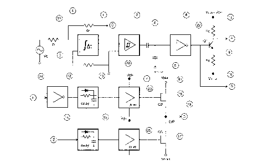
A Class D amplifier having a low-level audio signal feeding the negative input
of an Integrator
via an input resistor. Said Integrator feeds a Comparator having well-defined
Hysterisis. Said
Comparator output is connected to a First Level Shifter in order to convert a
ground-referenced
signal to a negative-voltage-rail-referenced signal so as to provide a drive
signal for a First
Switching Device which is connected to a Negative Rail Voltage (Vminus) and an
Output, where
said Output is defined as the junction of said First and a Second Switching
Device and said
junction having a time averaged signal of high power capable of driving a low
impedance load
such as a loudspeaker. A Second Level Shifter is provided so as to drive said
Second Switching
Device which is connected to the Positive Rail Voltage (Vplus) and said
Output. The signal from
said Second Level Shifter is floating and referenced to said Output. The
signal at said Output is
kept in phase with the signal of said Second Level Shifter, yielding very high
.DELTA.v/.DELTA.t immunity at said Output. A Feedback Resistor is provided
from said
Output to the negative input of said Integrator in order to ensure self
oscillation and to provide
negative feedback in order to reduce distortion and the effective output
impedance (increasing
the damping factor). A Low-Pass tilter between said Output and said Load is
desirable to reduce
unwanted RF and switching noise.


Claims

Note: Claims are shown in the official language in which they were submitted.


Claims
The embodiments of the invention in which an exclusive property or privilege
is claimed are
defined as follows:
1. A Class D amplifier, comprising:
a) a source of split DC voltage having a Negative Voltage Rail, a Positive
Voltage Rail and a
Ground,
b) an audio signal source connected to a First Input Resistor which is
connected to the negative
input of an Integrator,
c) a Comparator, having a well-defined Hysterisis, with its input connected to
said Integrator's
output,
d) a First Level Shifter comprising a First and a Second Capacitor connected
in series between
the output of said Comparator and the negative voltage rail so as to change
the Ground
Referenced Output Signal of said Comparator to said Negative Voltage Rail
Referenced signal,
e) said Negative Voltage Rail Referenced Signal at the junction of said First
and Second
Capacitor is connected to a First Buffer,
f) a Second Level Shifter utilizing a Transistor in a switched current source
configuration
wherein the signal derived from the collector of said transistor is floating
and referenced to the
output and is also in phase with the output signal achieving high
.DELTA.v/.DELTA.t immunity;
g) a First and a Second Asymmetrical Delay Network introducing the appropriate
amount of
delay in order to avoid simultaneous conduction,
7

h) a Second Buffer driven by the collector of said Transistor having low
output impedance in
order to drive said Second Asymmetrical Delay Network,
i) a First and a Second Output Switch driven by First and Second Driver stages
that deliver high
speed, high current pulses modulated by the signal from said audio signal
source, and the
junction of sail First and Second Switches is capable of driving a low
impedance load such as a
loudspeaker,
j) a First Feedback Resistor also connected between the negative input of said
Integrator, and the
Output obtained at the said junction of said First and Second Switches,
reducing non-linearities
and distortion so that the average value of the signal obtained at said Output
will be defined as
the value of said First Feedback Resistor divided by the value of the First
Input Resistor times
the Audio Input Signal.
2. A Class D amplifier circuit as claimed in claim 1, having an Input Resistor
that is connected to
an audio signal source and a Feedback Resistor connected to the negative input
of an Integrator,
wherein said Integrator has a Triangular waveform output signal.
3. A Class D amplifier circuit as claimed in claim 1, wherein said Comparator
has a well defined
Hysterisis which in turn will define the peak-to-peak value of said triangle
waveform
4. A Class D amplifier circuit as claimed in claim 1, wherein said First and
said Second
Capacitors of said First Level Shifter serve as a voltage divider of the
pulses that are generated at
the output of said Comparator and converting said pulses that are Ground
Referenced to pulses
that are Negative Voltage Rail Referenced.
5. A Class D amplifier circuit as claimed in claim 1, wherein said First
Buffer is utilized to drive
said First Asymmetrical Delay Network and said Second Level Shifter.
6. A Class D amplifier circuit as claimed in claim 1, wherein said First
Asymmetrical Delay
8

Network consists of a First Resistor, First Capacitor and is made asymmetrical
by means of
bypassing the first Resistor with First Switching Diode.
7. A Class D amplifier circuit as claimed in claim 1, wherein said Second
Asymmetrical Delay
Network consists of a Second Resistor, Second Capacitor and is made
asymmetrical by means of
bypassing the Second Resistor with Second Switching Diode.
8. A Class D amplifier circuit as claimed in claim 1, wherein said Second
Level Shifter includes
a Transistor configured as a switched current source in order to convert a
Negative Voltage Rail
Referenced Signal to an Output Referenced Signal.
9. A Class D amplifier circuit as claimed in claim 1, wherein said First
Driver stage is utilized to
deliver high speed, high current pulses to the gate of said First Output
Switch which is connected
to said Negative Voltage Rail and said Second Output Switch.
10. A Class D amplifier circuit as claimed in claim 1, wherein said Second
Driver stage is
utilized to deliver high speed high current pulses to the gate of said Second
Output Switch which
is connected to said Positive Voltage Rail and said First Output Switch.
11. A Class D amplifier circuit as in claim 1, wherein the positive input of
said Integrator is
connected to Ground via a Second Input Resistor paralleled with an Integrating
Capacitor and a
Second Feedback Resistor which is connected between said positive input of
said Integrator and
the output junction of a Third and Fourth Output Switches which are driven by
an identical drive
signal processing circuits as in claim 1 wherein the Output signal is defined
as that signal
appearing between the junction of said First and Second Output Switches and
the junction of said
Third and Fourth Output Switches; said Second Input Resistor should be chosen
to be equal in
value to said First Input Resistor and said Second Feedback Resistor should be
chosen to be
equal in value to said First Feedback Resistor to ensure that the two
amplifiers so connected have
equivalent gain, so as to allow a doubling of available average power while
maintaining
feedback for both amplifying stages.
9

12. Class D amplifier circuit as in claim 11, wherein the feedback signals
provided to the
negative and positive inputs of said Integrator will force the duty cycle of
the signal appearing at
said Output to be limited to a well defined value at the extremes of
modulation, which provides a
highly desirable feature in that it prevents the Class D amplifier of claim 11
from operating too
close to edge of modulation thus maintaining stability under all signal
conditions.

Description

Note: Descriptions are shown in the official language in which they were submitted.


CA 02274420 2002-02-13
Description
FIELD OF THE INVENTION
The present invention is related in general to high efficiency power
amplification. In particular, it
is related to the Class D type switching amplifier wherein voltage and current
stresses are never
simultaneously present, yielding efficiencies in the ~)0'%+ region. The
present invention achieves
this objective with the minimum number of inexpensive "off the shelf'
components while
maintaining a high degree of functionality and reliability.
BACKGROUND OF THE INVENTION
In the prior art as depicted in FIG. I, the low level aLrdio signal (8) is
injected into the input of a
Pulse Width Modulator ( 1 ) having a signal which is referenced to ground.
Said signal is then
referenced to a negative voltage rail with the aid of Level Shifter ('?). The
negative rail
referenced, pulse width modulated signal is typically fed to Driver (4) with
the aid of High Side
and Low Side Dead Zone (3) processing circuitry in order to avoid the
simultaneous conduction
of Output Switching Devices (6) and (7). Customarily a Feedback Resistor (9)
is employed
between Output (7) and the Pulse Width Modulator ( 1 ) in order to reduce non-
linearities.
FIG. 2 depicts the typical circuitry within Driver (F1G. 1 (4)). In the prior
art depicted in FIG. 2,
the Low and High Side Logic Level signals are fed to a pair of R/S Flip-Flops
( 1 ). The Signal
Output of said R/S Flip-Flops is then fed to Level Shiner (2) in order to
obtain a drive signal for
the high current output Low Side Drive (6).
The High Side high current Driver (5) is driven by (tlS Flip-Flop (~). The
input to said R/S Flip-
Flop (4) is also driven by another Level Shifter (3) to obtain a floating High
Side signal. Pulse
Generator (7) is introduced between Level Shifter (2) and Level Shiner (3) to
ensure noise

CA 02274420 2002-02-13
immunity and freedom from false triggering.
Level Shifter (3~) is the most critical in high voltage, high frequency
applications. The
simultaneous presence of high voltage and high frequency requirements will
introduce a thermal
component in addition to that produced by the High Side Driver (5) and Low
Side Driver (6).
The two thermal components can be computed as CV<sup>2</sup> F. Said two thermal
components will
limit the Power-Frequency product to approximately 125,000 WkE-Iz.
The present invention exhibits a constant thermal component in respect to
frequency, total
freedom from false triggering, and a Power-Frequency product of 125,000 WkHz.
In its most common form, the functionality described above is implemented in a
commercially
available high density Integrated Circuit. FIG. 2 and the above description
shows the large
number of signal processing stages that said Pulse Width Modulated signal
obtained at the output
of the High Side and Low Side Dead Zone processing circuitry (FIG. 1 (3)) has
to undergo.
The large number of said signal processing stages depicted in Driver (4)
result in propagation
delays in excess of the 100 nS range. For a (:lass D amplifier of relatively
high power, say 200W
into 8.OMEG,A,., a 100 kHz switching frequency can not be exceeded without
impairing
reliability. However, a 100 kHz switching frequency yields unacceptably high
distortion in the
higher registers, of the audio band. A further limiting factor is the maximum
DELTA.v/.DELTA.t that can be obtained at the Output (7) without causing false
triggering. A
false triggering condition can lead to destruction of the Output Switching
Devices (5) and (6).
The present invention overcomes the complexity and high cost of the prior
solution by achieving
the same functionality using discrete, inexpensive, "ofd the-shelf' components
while
simultaneously increasing the flexibility of the resulting circuits, allowing
the same topology to
satisfy requirennents from SOWRMS to over 100WRMS. Most importantly, the
present invention
allows higher switching speeds while improving reliability through superior
DELTA.v/.DELTA.t immunity Typically, one may obtain a switching speed with no
loss of
reliability up to~ 5 MHz at 40V and 500 kHz at 200V.

CA 02274420 2002-02-13
Matching the propagation delays of the High Side and Low Side Drives is not a
critical issue in
the present invention as these are readily adjusted by appropriately choosing
the component
values of the Asymmetrical Delay Networks.
BRIEF DESCR;1PTION OF THE DRAWINGS
The present invention will now be described, by way of example only, with
reference to the
following drawings in which:
FIG. I is a schE;matic diagram of the components of a prior art Class D
amplifier;
FIG. 2 is a schematic diagram of the circuit layout of a driver of the Class D
amplifier of FIG. I;
FIG. 3 shows in diagrammatic form the circuit layout of a Class D amplifier
made in accordance
with the preferred embodiment of the present invention; and
FIG. 4 shows in diagrammatic form the circuit layout of a full bridge Class D
amplifier made in
accordance with an alternate embodiment of the present invention.
DETAILED DESCR1PTION OF THE PREFERRED EMBODIMENT
FIG. 3 shows the preferred embodiment of a Class D amplifier utilizing the
present invention.
Signal Generator (3) is fed to the negative input of Integrator ( 1 ) through
Input Resistor (18). A
Feedback Resistor (4) is also connected from the Output (19) to said negative
input. The signal
from Integrator ( 1 ) is an input for the Comparator (2) that has a Hysterisis
which can be used to
set the frequency of self oscillation of the Class D amplifier. The signal at
the output of
Comparator (2) is referenced to Ground (20) and is therefore not suitable to
drive directly the
output devices ~Q2 (I6) and Q3 (17).
To obtain a Nel;ative Rail Voltage (5) referenced signal a capacitive level
shifter is utilized

CA 02274420 2002-02-13
consisting of C',apacitor (6) and Capacitor (7) that are connected in series.
Capacitor (7) is
connected to Vminus (5) and the other side, which is the junction of the two
capacitors, is fed to
First Buffer (8). The other side of Capacitor (6) is connected to the
Comparator (2) output. The
output of said E~irst Buffer (8) is connected to Transistor (9) base. The
emitter of said Transistor
(9) is connected to Vminus(5) through an Emitter Resistor ( 10) so as to
produce a switched
current source. The collector of said Transistor (10) is connected to the
Positive Rail Voltage (5)
incremented by gate supply voltage, Vplus+-VgH (22), through a Collector
Resistor ( l l). The
signal appearing at the collector of Transistor (9) will float with the output
signal. This is then
fed to Second I3uf~er (24) driving a First Asymmetrical Delay Network { 12)
which is then fed to
input of Mosfet Driver ( l3). The output obtained at Mosfet Driver ( 13) thus
will have sufFcient
current driving capabilities for Switching Device (1G). Similarly the signal
generated at the
output of Butler (8) is fed to the input of Second Asymmetrical Delay Network
( 14) and the
output of said Second Asymmetrical Delay Network ( 14) is fed to the Mosfet
Driver (1 S) which
also has high current switching capability.
The timing of the switching sequence is set by First and Second Asymmetrical
Detay Networks
(12) and (14) and will insure that no cross-conduction will take place between
Output Switching
Devices ( 16) and (17). The signal gain will be defined by the ratio of the
values of said Feedback
Resistor (4) and said Input Resistor (18).
FIG. 4 shows an alternative embodiment for which the present art is
particularly well suited.
Class D amplifiers offer the greatest advantage for high power applications,
where their
et~ciency can translate into cost savings in power supply and heat sink
components. Therefore a
Full Bridge configuration is highly desirable. However, in such a
configuration, in order to
remove non-linearities, a feedback loop would have to be incorporated which
includes both
output stages. Said feedback loop is readily achieved in the present invention
by connecting
another Feedback Resistor from the Second Output Stage to the positive input
of the Integrator.
Illustrated in FIG. 4 is a Fult Bridge Class D Amplifier with negative
feedback around both
outputs. Signal Generator ( 13) is connected through First input Resistor ( I
) to the negative input
of integrator (5). A Second Input Resistor (3) is connected between the
positive input of said

CA 02274420 2002-02-13
Integrator (5) and ground. An integrating Capacitor (;14) is connected is also
connected from said
positive input to the ground. The output of said Integrator is fed to Class D
Drive (6). The output
of said Class D Drive (6) supplies the high current required to switch the set
of Output Devices
(11) & (12). Another output is derived from said Class D Drive (6) which is
connected to the
input of Inverter (8) so as to a 180° phase shift between the output
signal of the First &
Second Output Stages. Class D Drive (?) has a similarly high current output to
ensure rapid
switching of Switching Devices (9) & ( 10).
Feedback Resistor (15) is connected between the negative input of Integrator
(5) and the junction
of Switching Devices (11) & (12). Feedback Resistor (4) is connected between
the positive input
of Integrator (5) and the junction of Switching Devices (9) & (10).
If Feedback Resistors (4) & (IS) are chosen to be equal in value, and Input
Resistors (1) & (3)
are also of equal value, then the total gain is derived by the Feedback
Resistance divided by the
Input Resistance.
Thus, while what is shown and described herein constitutes preferred
embodiments of the subject
invention, it should be understood that various changes can be made without
departing from the
subject invention, the scope of which is defined in the appended claims.
e>

Representative Drawing
A single figure which represents the drawing illustrating the invention.
Administrative Status

2024-08-01:As part of the Next Generation Patents (NGP) transition, the Canadian Patents Database (CPD) now contains a more detailed Event History, which replicates the Event Log of our new back-office solution.

Please note that "Inactive:" events refers to events no longer in use in our new back-office solution.

For a clearer understanding of the status of the application/patent presented on this page, the site Disclaimer , as well as the definitions for Patent , Event History , Maintenance Fee  and Payment History  should be consulted.

Event History

Description Date
Time Limit for Reversal Expired 2013-05-31
Inactive: Adhoc Request Documented 2013-03-04
Letter Sent 2012-05-31
Inactive: Late MF processed 2010-05-26
Inactive: Office letter 2009-09-24
Inactive: Payment - Insufficient fee 2009-09-24
Letter Sent 2009-06-01
Change of Address or Method of Correspondence Request Received 2009-02-06
Inactive: Late MF processed 2008-09-29
Letter Sent 2008-06-02
Inactive: Office letter 2007-11-06
Inactive: Office letter 2007-10-17
Inactive: Late MF processed 2007-07-20
Letter Sent 2007-05-31
Inactive: IPC from MCD 2006-03-12
Change of Address Requirements Determined Compliant 2005-02-02
Inactive: Office letter 2005-02-02
Change of Address or Method of Correspondence Request Received 2005-01-19
Change of Address or Method of Correspondence Request Received 2004-01-26
Change of Address or Method of Correspondence Request Received 2003-12-08
Grant by Issuance 2002-10-15
Inactive: Cover page published 2002-10-14
Inactive: Inventor deleted 2002-09-19
Inactive: Applicant deleted 2002-09-19
Inactive: Inventor deleted 2002-09-19
Inactive: Final fee received 2002-07-30
Pre-grant 2002-07-30
Notice of Allowance is Issued 2002-03-22
Letter Sent 2002-03-22
Notice of Allowance is Issued 2002-03-22
Inactive: Approved for allowance (AFA) 2002-03-13
Amendment Received - Voluntary Amendment 2002-02-13
Inactive: S.30(2) Rules - Examiner requisition 2001-10-16
Change of Address or Method of Correspondence Request Received 2001-10-03
Amendment Received - Voluntary Amendment 2001-08-20
Inactive: S.30(2) Rules - Examiner requisition 2001-05-18
Letter sent 2001-04-20
Advanced Examination Determined Compliant - paragraph 84(1)(a) of the Patent Rules 2001-04-20
Request for Examination Received 2001-04-05
Request for Examination Requirements Determined Compliant 2001-04-05
Inactive: Advanced examination (SO) fee processed 2001-04-05
All Requirements for Examination Determined Compliant 2001-04-05
Inactive: Advanced examination (SO) 2001-04-05
Inactive: Office letter 2001-01-10
Inactive: Applicant deleted 2001-01-10
Inactive: Compliance - Formalities: Resp. Rec'd 2000-12-08
Inactive: Delete abandonment 2000-12-04
Application Published (Open to Public Inspection) 2000-11-30
Inactive: Cover page published 2000-11-29
Inactive: Status info is complete as of Log entry date 2000-10-12
Inactive: Abandoned - No reply to Office letter 2000-09-01
Inactive: Correspondence - Formalities 1999-09-17
Inactive: Filing certificate - No RFE (English) 1999-09-17
Inactive: Correspondence - Formalities 1999-09-03
Inactive: First IPC assigned 1999-08-03
Inactive: Applicant deleted 1999-07-29
Inactive: Filing certificate - No RFE (English) 1999-07-16
Application Received - Regular National 1999-07-15
Small Entity Declaration Determined Compliant 1999-05-31

Abandonment History

There is no abandonment history.

Maintenance Fee

The last payment was received on 2001-05-15

Note : If the full payment has not been received on or before the date indicated, a further fee may be required which may be one of the following

  • the reinstatement fee;
  • the late payment fee; or
  • additional fee to reverse deemed expiry.

Patent fees are adjusted on the 1st of January every year. The amounts above are the current amounts if received by December 31 of the current year.
Please refer to the CIPO Patent Fees web page to see all current fee amounts.

Fee History

Fee Type Anniversary Year Due Date Paid Date
Application fee - small 1999-05-31
2000-12-08
Advanced Examination 2001-04-05
Request for examination - small 2001-04-05
MF (application, 2nd anniv.) - small 02 2001-05-31 2001-05-15
MF (application, 3rd anniv.) - small 03 2002-05-31 2001-05-15
Final fee - small 2002-07-30
MF (patent, 4th anniv.) - small 2003-06-02 2003-04-11
MF (patent, 5th anniv.) - small 2004-05-31 2004-05-03
MF (patent, 6th anniv.) - small 2005-05-31 2005-05-24
MF (patent, 7th anniv.) - small 2006-05-31 2006-05-29
Reversal of deemed expiry 2009-06-01 2007-07-20
MF (patent, 8th anniv.) - small 2007-05-31 2007-07-20
MF (patent, 9th anniv.) - small 2008-06-02 2008-09-29
Reversal of deemed expiry 2009-06-01 2008-09-29
MF (patent, 10th anniv.) - small 2009-06-01 2009-09-04
Reversal of deemed expiry 2009-06-01 2009-09-04
MF (patent, 11th anniv.) - small 2010-05-31 2010-05-28
MF (patent, 12th anniv.) - small 2011-05-31 2011-05-31
Owners on Record

Note: Records showing the ownership history in alphabetical order.

Current Owners on Record
IVAN MESZLENYI
Past Owners on Record
None
Past Owners that do not appear in the "Owners on Record" listing will appear in other documentation within the application.
Documents

To view selected files, please enter reCAPTCHA code :


To view images, click a link in the Document Description column. To download the documents, select one or more checkboxes in the first column and then click the "Download Selected in PDF format (Zip Archive)" or the "Download Selected as Single PDF" button.

List of published and non-published patent-specific documents on the CPD .

If you have any difficulty accessing content, you can call the Client Service Centre at 1-866-997-1936 or send them an e-mail at CIPO Client Service Centre.


Document
Description 
Date
(yyyy-mm-dd) 
Number of pages   Size of Image (KB) 
Description 1999-05-30 4 212
Abstract 1999-05-30 1 51
Claims 1999-05-30 4 150
Drawings 1999-05-30 4 67
Abstract 2001-08-19 1 35
Description 2001-08-19 6 220
Claims 2001-08-19 4 159
Abstract 2002-02-12 1 42
Claims 2002-02-12 4 145
Description 2002-02-12 5 234
Representative drawing 2000-11-20 1 12
Filing Certificate (English) 1999-07-15 1 165
Filing Certificate (English) 1999-09-16 1 174
Request for evidence or missing transfer 2000-05-31 1 110
Notice: Maintenance Fee Reminder 2001-02-28 1 120
Commissioner's Notice - Application Found Allowable 2002-03-21 1 166
Notice: Maintenance Fee Reminder 2003-03-02 1 122
Notice: Maintenance Fee Reminder 2004-03-01 1 116
Notice: Maintenance Fee Reminder 2005-02-28 1 119
Notice: Maintenance Fee Reminder 2006-02-28 1 119
Notice: Maintenance Fee Reminder 2007-02-28 1 118
Maintenance Fee Notice 2007-07-11 1 172
Late Payment Acknowledgement 2007-11-05 1 164
Notice: Maintenance Fee Reminder 2008-03-02 1 122
Maintenance Fee Notice 2008-07-13 1 171
Late Payment Acknowledgement 2008-10-08 1 164
Notice: Maintenance Fee Reminder 2009-03-02 1 120
Maintenance Fee Notice 2009-07-12 1 171
Notice of Insufficient fee payment (English) 2009-09-23 1 91
Second Notice: Maintenance Fee Reminder 2009-11-30 1 118
Notice: Maintenance Fee Reminder 2010-03-01 1 122
Late Payment Acknowledgement 2010-06-06 1 163
Notice: Maintenance Fee Reminder 2011-02-28 1 120
Notice: Maintenance Fee Reminder 2012-02-29 1 119
Maintenance Fee Notice 2012-07-11 1 171
Second Notice: Maintenance Fee Reminder 2012-12-02 1 118
Notice: Maintenance Fee Reminder 2013-03-03 1 121
Correspondence 2003-12-07 1 21
Correspondence 2002-03-21 1 56
Correspondence 2002-07-29 1 54
Correspondence 2001-10-02 2 87
Fees 2001-05-14 1 133
Correspondence 1999-07-19 1 46
Correspondence 1999-09-02 1 39
Correspondence 1999-09-16 2 59
Correspondence 2000-02-28 1 35
Correspondence 2000-12-03 1 16
Correspondence 2000-12-07 1 24
Correspondence 2001-01-09 1 8
Fees 2004-05-02 1 125
Correspondence 2005-01-25 3 84
Correspondence 2005-01-18 1 30
Correspondence 2005-02-01 1 19
Fees 2005-05-23 1 76
Fees 2006-05-28 1 45
Correspondence 2007-10-16 1 14
Correspondence 2007-11-05 2 61
Fees 2007-07-19 1 26
Fees 2008-09-28 1 30
Correspondence 2009-02-05 1 28
Correspondence 2009-09-23 1 19
Fees 2009-09-03 1 31
Fees 2009-09-23 1 22
Fees 2009-09-23 1 21
Fees 2010-05-25 1 32
Fees 2010-05-27 1 31
Fees 2011-05-30 1 28