Note: Descriptions are shown in the official language in which they were submitted.
CA 02274529 1999-06-08
WO 98/33272 PCT/US97/23657
HIGH DYNAMIC RANGE VARIABLE GAIN AMPLIFIER
BACKGROUND OF THE INVENTION
I. Field of the Invention
The present invention relates to variable gain amplifiers (VGAs) and
particularly to VGAs used in communication devices.
II. Description of the Related Art
In a wireless communication environment, a wireless
communications receiver may receive a signal -which experiences rapid and
wide variations in signal power. In receivers such as are used in a wideband
digital code division multiple access (CDMA) mobile station, it is necessary
to control the power of the demodulated signal for proper signal processing.
Furthermore, in transmitters such as are used in a CDMA mobile station, it
is necessary to control the transmit power in order to avoid excessive
interference to other mobile stations. These same power control
considerations apply to narrowband analog frequency modulation (FM)
wireless communication system receivers and transmitters.
Dual-mode CDMA/FM wireless communications devices exist which
are required to provide power control of transmitted and received signals of
both digital CDMA and analog FM modulation. In these dual-mode mobile
stations, the control process is complicated by the differing dynamic ranges
and industry regulation standards associated with the CDMA and FM
signals. That is, the magnitude of the received CDMA signals may vary over
a range of approximately 80 dB, whereas the magnitude of the received FM
signals may vary over a range of as much as 100 dB. The provision of
separate automatic gain control (AGC) circuitry for both the CDMA and the
FM signals increases the complexity and expense of such dual-mode mobile
stations. Accordingly, it is desirable to provide AGC circuitry capable of
operating upon both the CDMA and FM signals.
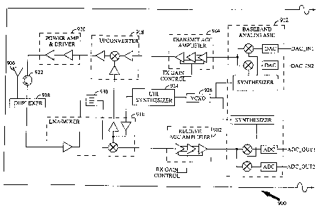
FIGS. 1A and 1B illustrate an exemplary environment for a VGA
performing AGC functions. FIGS. 1A and 1B are a block diagram of a dual
mode CDMA/FM cellular telephone 900 designed, for example,, in
accordance with the telecommunication industry standard "Mobile Station
Base Station Compatibility Standard for Dual-Mode Wideband Spread
Spectrum Cellular System," TIA/EIA/IS-95, generally referred to simply as
IS-95.. A VGA is used for receive and transmit AGC amplifiers 902, 904
respectively, of cellular telephone 900. The front end receiver portion of
CA 02274529 1999-06-08
WO 98/33272 PCT/L1S97/23657
2
cellular telephone 900 comprises antenna 906, duplexer 908, low noise
amplifier (LNA) and mixer circuit 910, and filter 930. As cellular
telephone 900 travels throughout the coverage area of a CDMA system, the
signal level at antenna 906 varies from about -110 dBm to - 30 dBm. Note
that each of these front end elements generally provides the same gain no
matter what signal level is applied to it over the operating range such that
the dynamic range of the signal which is applied to receive AGC
amplifier 902 is the same as the dynamic range of the signal at antenna 906,
approximately 80 dB. Similarly, when the cellular telephone 900 travels
throughout the coverage area of an FM system, the signal level at the
antenna varies approximately 100 dB.
The output of receive AGC amplifier 902 is provided to baseband
analog application specific integrated circuit (BAASIC) 912 which converts
the analog signal to a digital signal. The analog to digital signal conversion
process works best if the signal level which is applied to the analog to
digital
converter remains constant. Receive AGC amplifier 902 performs the
function of compensating for the variations input power such that the
output power of receive AGC amplifier 902, and thus the input to the analog
to digital converter, remains constant.
Mobile station modem ASIC 914 provides demodulation for both the
CDMA and FM signals, as well as various digital and power control
functions associated with CDMA operation. Such functions are well known
in the art and not critical to the present invention, and thus are not
described further herein. User interfaces 916 provide the interface to the
human operator. Such user interfaces 916 are also well known in the art
and not critical to the present invention, and are thus not described further
herein.
Mobile station modem ASIC 914 also provides a baseband modulated
digital representation of the CDMA waveform, or a modulated analog
representation of the FM waveform to BAASIC 912. BAASIC 912 converts
the baseband signals representation to analog intermediate frequency (IF)
form at a constant signal level and supplies it to transmit AGC amplifier 904.
Transmitter AGC amplifier 904 provides power control to the signal and
supplies it to upconverter 918, power amplifier and driver circuitry 920,
isolator 922, duplexer 908 and antenna 906. As cellular telephone 900 travels
throughout the coverage area of a cellular system, the transmit signal level
at antenna 906 varies inversely from receive power in that when the receive
power is at a minimum the transmit level is near the maximum. This
variation in transmit power level is accomplished by AGC amplifier 904.
__...~..~.~. T T .. ..... _ .~ _
CA 02274529 1999-06-08
WO 98/33272 PCT/US97/23657
3
Note that the input power to AGC amplifier 904 is typically fixed, and the
gain of power amplifier 920 may also be fixed.
More information about the automatic gain control loop in a wireless
communication system and about power control in general can be found l n
U.S. Patent No. 5,283,536, entitled "HIGH DYNAMIC RANGE CLOSED
LOOP AUTOMATIC GAIN CONTROL CIRCUIT" issued February 1, 1994,
U.S. Patent No. 5,107,225, entitled "HIGH DYNAMIC RANGE CLOSED
LOOP AUTOMATIC GAIN CONTROL CIRCUIT" issued April 21, 1992, U.S.
Patent No. 5,267,262 entitled "TRANSMITTER POWER CONTROL
SYSTEM" issued November 30, 1993, U.S. Patent No. 5,469,115 entitled
"METHOD AND APPARATUS FOR AUTOMATIC GAIN CONTROL IN A
DIGITAL RECEIVER" issued November 12, 1995 and U.S. Patent No.
5,283,536 entitled "HIGH DYNAMIC RANGE CLOSED LOOP AUTOMATIC
GAIN CONTROL CIRCUIT" issued October 26, 1993, each of which is
assigned to the assigned hereof and incorporated herein by reference.
Mobile communication receivers and transmitters like those
described above are designed to have a high compression point, low noise
injection and low power consumption. Receivers with a high compression
point and low noise injection have a high dynamic range in that they can
detect signals over a wide range of power levels. Transmitters with a high
compression point and low noise injection have a high dynamic range in
that they can transmit signals over a wide range of power levels. Receivers
and transmitters with low power consumption increase battery life. Hence,
these characteristics are important when designing a variable gain amplifier
for a communication system in which signals are transmitted and received
over a large range of power levels.
A receiver should be able to detect information from both a strong
signal broadcast by a nearby and powerful transmitter and a weak signal
broadcast by a distant and low power transmitter. The extent over which the
receiver can detect weak to strong signals is termed its dynamic range.
Likewise, a transmitter should be able to transmit low powered signals to a
nearby receiver and high power signals to a distant receiver.
The dynamic range of a receiver is established by its minimum
detectable and maximum detectable signal levels. The minimum detectable
signal Ievel of a receiver is determined by the receiver's noise figure.
Likewise the minimum transmittable power is set by the transmitters noise
figure if the signal level falls near or below the noise floor. A VGA's noise
figure is in part a function of the noise injection properties and gain of the
CA 02274529 1999-06-08
WO 98/33272 PCT/US97/23657
4
VGA. In general, the higher the receiver's gain, the better it's noise figure;
i.e. the better able it is to detect a very weak signal in the presence of
noise.
The maximum detectable signal level of a receiver may be established
by the receiver's intermodulation distortion (IMD) performance. When
multiple signals pass through any device, mixing action between the signals
occurs because of the non-linearities of the device. For example, in a
location where CDMA and analog FM systems co-exist, third-order IM
products from the analog FM system generally fall within the CDMA
passband. This IM products act as "jammers" that contribute to IMD which
can interfere with detection and demodulation of the desired signal within
the receiver. A VGA's IMD performance is in part a function of its linearity
and its gain. In general, the lower the receiver's gain, the better it's IMD
performance. This is in contrast to the noise figure requirements as
described above. Thus, design of a VGA for a receiver with a large dynamic
range includes the difficult tradeoff between IMD performance and noise
figure.
Similar design considerations are relevant with respect to transmitter
VGAs, with the difference being that generally, receiver VGAs are designed
to provide a relatively constant output power level for a varying range of
input power levels while transmitter VGAs are designed to receive
relatively constant input power levels and provide a varying range of
output power levels.
Furthermore, mobile receivers are designed to be compact,
lightweight, and have a long operating lifetime. Mobile receivers are
powered by a minimal number of battery cells to reduce their size and
weight to enhance their portability. Because battery voltage is proportional
to the number of battery cells, the AGC circuitry, including the variable gain
amplifier (VGA}, must operate at low supply voltages. It is also desirable to
enhance battery lifetime in order to increase the period between battery
replacement or recharging. Therefore, the AGC circuitry, including its VGA,
should consume little DC current and power.
This requirement for low DC power consumption also implies a
design tradeoff similar to that already mentioned. More DC power is
required for a high gain amplifier that has good noise figure. However, less
DC power is required for a low gain amplifier that has good IMD
performance. Existing VGA designs are inefficient in that they are unable to
conserve DC power sufficiently at low gain levels.
What is needed is a VGA with a high dynamic range, good noise
figure and IMD performance, as well as low DC power consumption.
____ __T T _.__ ..~..__. _ . _
CA 02274529 1999-06-08
WO 98/33272 PCTlUS97/23657
SUMMARY OF THE INVENTION
In accordance with the present invention, there is provided a VGA
having a high dynamic range, good noise figure and IMD performance, and
5 minimal DC power consumption. The VGA may be used in automatic gain
control (AGC) amplifiers for the receiver and transmitter chains in a cellular
telephone. The VGA achieves power gain by converting an input voltage
signal to a current signal and amplifying the current signal. The amplified
current signal may be converted to a voltage signal by terminating the VGA
with an appropriate impedance.
The VGA is comprised of at least two cascaded stages, an input stage
and a current amplifier. The input stage may be further separated into a
CDMA input stage and an FM input stage, with the outputs of both input
stages being coupled to the input of the current amplifier, and being
selectable by a CDMA/FM mode signal. In one embodiment, the FM input
stage is single-ended, and the CDMA input is balanced. The gain of the VGA
may be increased by successively cascading two or more current amplifier
stages. The transconductance gain of the input stages may be controlled by a
control signal.
The high dynamic range, low power VGA is made using a
combination of techniques. In a first embodiment, well suited for a dual-
mode receive AGC amplifier such as amplifier 902 of FIG. 1, the CDMA
input stage is comprised of a variable transconductance amplifier cascaded
with a Gilbert cell attenuator. The variable transconductance amplifier
converts a varying voltage signal to an output current signal with a
transconductance that is controlled by a FET transistor acting as a variable
emitter degeneration resistor. The emitter degeneration provides variable
local series feedback which allows the CDMA input stage to handle a wide
dynamic range of input signals, while providing good noise figure and IMD
performance. In the presence of a low level input signal, the channel
resistance of the FET transistor may be varied to increase the gain of the
input stage, thereby improving the receiver's noise figure and ability to
detect weak signals. On the other hand, in the presence of a high level input
signal, the channel resistance of the FET transistor may be varied to decrease
the gain of the input stage, thereby improving the receiver's IMD
performance. The Gilbert cell attenuator provides additional current
attenuation so that any later current amplification stages to not get
overdriven into their non-linear range when a large input signal is applied.
CA 02274529 1999-06-08
WO 98/33272 PCT/US97/23657
6
In this first embodiment, the FM input stage is a bipolar differential
amplifier with emitter degeneration, followed by a Gilbert cell attenuator.
The differential pair converts the input voltage to a current and feeds the
Gilbert cell attenuator, which further attenuates the current flowing into the
next stage of the current amplifier. Unlike the CDMA input stage, the FM
input stage uses a fixed gain transconductance stage rather than variable
emitter degeneration because the industry standard (IS-95) linearity
requirement for FM signals is much more relaxed than that for CDMA
signals, allowing the amplifier to saturate into non-linearity much sooner.
In a second embodiment, well suited for a transmit AGC amplifier
such as amplifier 904 of FIG. 1, both FM and CDMA signals may be handled
by an fixed-gain transconductance input stage comprising a differential pair
with shunt-series feedback at the input, followed by a transconductor and
Gilbert cell attenuator. The shunt-series feedback at the input allows for an
accurate and linear input impedance without using a brute force match. The
output of the differential pair may be AC coupled to the transconductor by a
pair of capacitors. The transconductor converts the voltage output of the
differential pair to a current using an emitter-degenerated differential
amplifier. The current is then fed to the Gilbert cell attenuator which
further attenuates the current flowing into the next stage of the current
amplifier. A variable gain input stage is not required because the input level
to the transmit AGC amplifier 904 is generally constant.
In the first embodiment, suited for use as receive AGC amplifier 902,
each of the current amplifiers are comprised of two sections, a differential
Darlington amplifier and a differential cascode amplifier. These current
amplifiers are translinear circuits which allow the current gain to be
controlled by varying the ratio of the "tail currents" which bias the
translinear loop. The current gain of each current amplifier stage may be
independently controlled by one or more control signals.
In the second embodiment, suited for use as a transmit AGC amplifier
904, each of the current amplifiers is comprised of two sections, a
differential
Darlington amplifier, and a simple differential pair. This current amplifier
is a hybrid of a feedback current amplifier and a translinear loop.
In each of the above-mentioned embodiments, the gain of the
variable-gain stages is controlled by a gain control circuit which varies the
gain of the current amplifiers according to the AGC control voltage applied
(either RX GAIN CONTROL or TX GAIN CONTROL of FIG. 1). The gain
control circuit includes an exponential function generator which ensures
the linearity (in dB) of the VGA over the wide dynamic range.
CA 02274529 1999-06-08
WO 98/33272 PCT/US97123657
7
It is accordingly a benefit of the present invention to provide a VGA
that has a high dynamic range over both CDMA and FM signals. A mobile
receiver utilizing such a VGA can detect signals over wider input power
ranges. A further benefit is that the VGA consumes minimal DC power.
Therefore, the VGA may be used in a mobile communication device and
advantageously conserve the operating lifetime of the batteries. An
additional benefit is that the VGA's gain can be varied approximately
linearly in dB by linearly adjusting DC control voltages.
BRIEF DESCRIPTION OF THE DRAWINGS
The features, objects, and advantages of the present invention will
become more apparent from the detailed description set forth below when
taken in conjunction with the drawings in which like reference characters
identify correspondingly throughout and wherein:
FIGS. 1A and 1B are a schematic diagram of an exemplary dual-mode
CDMA/FM communication device capable of use with the present
invention;
FIG. 2 is a block diagram of an exemplary triple stage variable gain
amplifier of the present invention;
FIG. 3 is a diagram of the CDMA input stage of FIG. 2;
FIG. 4 is a diagram of the transconductance amplifier bias control
circuit of FIG 2.;
FIG. 5 is a diagram of the exponential function generator of FIG. 4;
FIG. 6 is a partial combination of elements in FIGS. 2 and 3
constructed to illustrate the beneficial properties of the present invention;
FIG. 7 is a diagram of the current amplifiers of FIG. 2; and
FIG. 8 is a diagram of the tail current generator of FIG. 7.
DETAILED DESCRIPTION OF THE PREFERRED
EMBODIMENTS
The present invention is directed to a monolithic integrated circuit
variable gain amplifier (VGA). The VGA provides gain in proportion to a
control voltage. The VGA provides exponential voltage gain as a function
of linear increases in the applied control voltage thereby providing
approximately linear power gain in decibels (dB) in direct proportion to
linear increases in applied control voltage. The VGA can provide linear
power gain over a large dynamic range in excess of 80 dB (or a factor of 1 to
CA 02274529 1999-06-08
WO 98/33272 PCT/LJS97/23657
8
100,000,000.) The VGA provides a linear power gain which is tolerant of
process variations which occur during VGA fabrication.
The VGA can be used in many applications including in receivers and
transmitters. If the VGA is functioning in a receiver, the input to typically
varies over a large dynamic range while the output of the VGA is relatively
constant. When the signal level input into the VGA functioning in a
receiver is small the gain of the VGA must be relatively large. When the
signal Ievel input into the VGA functioning in a receiver is large, the gain
of
the VGA must be relatively small. Thus a VGA functioning in a receiver
must typically have good noise performance when it is providing relatively
high gain and good intermodulation performance when providing
relatively low gain.
If the VGA is functioning in a transmitter, the input is typically
constant while the output of the VGA varies over a wide dynamic range.
When the signal level output of the VGA needs to be large, the gain of the
VGA must be relatively large and the intermodulation performance must
support the resulting large signal levels. When the signal level output from
the VGA functioning in a transmitter needs to be small, the gain of the VGA
must be relatively small and the noise performance of the VGA may be
important.
FIG. 2 is a block diagram of one embodiment of variable gain
amplifier (VGA) 100 that adjusts the power level an input signal over a wide
dynamic range. The embodiment of FIG. 2 is suitable for use as receive AGC
amplifier 902 of FIG. 1. VGA 100 comprises three stages: input stage 120 and
two cascaded current amplifier stages 160A and 160B. More than one current
amplifier stage 160 is successively cascaded after input stage 120 to increase
the dynamic range of VGA 100. In a first embodiment, input stage 120
comprises a separate FM input stage 121 and CDMA input stage 122 with
respective input ports 171 and 170. FM input stage 121 and CDMA input
stage 122 are alternately connected to current amplifier 160A through
switches 123, which are controlled by the CDMA/FM mode select signal.
When the communication device is in CDMA mode, the switches 123
connect the CDMA input stage 122 to the current amplifier 160A and
disconnect the FM input stage 121. Conversely, when the communication
device is in the FM mode, the switches 123 connect the FM input stage 121 to
current amplifier 160A and disconnect the CDMA input stage 122.
FIG. 2 also illustrates bias ports 110, 130, 150A, 150B for the control
voltages to be applied to VGA 100. The gain of each stage is controlled by
control voltages which, for example, may be generated by receiver detection
T T ___.._. ._ . _.. .._~._
CA 02274529 1999-06-08
WO 98/33272 PCT/US97/23657
9
circuitry that determines the signal strength. Each stage is comprised of a
variety of components, including an active device such as a transistor.
The VGA input signal provided on input ports 170 of CDMA input
stage 122 is balanced, i.e. split into two signal paths each carrying a signal
one
hundred and eighty degrees out of phase from the another. The VGA input
signal is injected via VGA's input port 170. However, the VGA input signal
provided on input ports 171 of FM input stage 121 is single-ended. The
output of input stage 120 and the input of current amplifier 160A are
coupled through port 190.
Because it operates with a low supply voltage, about 3.6 volts, input
stage 120 converts the input voltage signal to a current signal to prevent the
VGA active devices from operating in their non-linear region, and
distorting the input signal. The low supply voltage of VGA 100 also reduces
the power consumption of VGA 100.
FIG. 3 illustrates one embodiment of the CDMA input stage 122. The
balanced signal is injected into VGA's input port 170. CDMA input stage 122
comprises variable transconductance amplifier 227 coupled to Gilbert cell
attenuator 226 and serves four functions. First, the variable
transconductance amplifier 227 converts the input voltage signal to a
current signal. Second, the combination of the variable transconductance
amplifier 227 and Gilbert cell attenuator 226 permits variable amplification
of the signal, which may be varied exponentially (linearly in dB) by linearly
adjusting control voltages at bias port 110. Third, increased emitter
degeneration in variable transconductance amplifier 227 reduces the IMD of
VGA 100 when the input signal voltage is large and the IMD would be most
prominent. As emitter degeneration in the variable transconductance
amplifier 227 is increased, the transconductance, and thus the IMD, of input
stage 120 are decreased. Finally, decreased emitter degeneration in variable
transconductor amplifier 227 improves the noise figure of VGA 100 when
the input signal voltage is small and noise performance is the most critical.
As emitter degeneration in variable transconductance amplifier 227 is
decreased, the transconductance of the input stage 120 is increased,
improving the noise figure of the receiver.
Variable transconductance amplifier 227 is comprised of two bipolar
junction transistors (BJTs) 235 and 236, two current sources 238, 239, and
field effect transistor (FET) 237. Current sources 238, 239 are serially
connected to the emitters of the BJTs 235 and 236. Source connection 228
and drain connection 229 of FET 237 are respectively connected to the
emitters of the BJTs 235 and 236 . The balanced signal at VGA input port 170
CA 02274529 1999-06-08
WO 98/33272 PCTIUS97/23657
is applied to the bases of BJTs 235 and 236. The balanced current output of
variable transconductance amplifier 227 flows from the collectors of the BJTs
235 and 236.
The transconductance of variable transconductance amplifier 227 may
5 be adjusted by varying the emitter degeneration of BJTs 235 and 236. As a
result, the gain of VGA 200 may be varied. Emitter degeneration of BJTs 235
and 236 is created by varying the channel resistance of FET 237: The FET 237
is operated like a variable resistor in its ohmic region and provides variable
emitter degeneration for both BJTs 235 and 236 . The drain-source bias
10 voltage of the FET 237 must therefore be less than the knee voltage of the
FET 237. The channel resistance may be varied by adjusting the bias across
the gate-source junction of the FET 237 by varying the voltage applied at bias
port 290. The transconductance of variable transconductance amplifier 227
can be increased by decreasing the channel resistance of the FET 237. Thus,
the present invention, by providing the variable channel resistance through
FET 237 allows both the competing design considerations of noise figure and
IMD performance to be accommodated. Furthermore, the DC efficiency of
the VGA 100 is improved because the CDMA input stage 122 draws enough
DC current as is necessary to amplify low level input signals, while reducing
the DC current consumption of later current amplification stages when
lowering its transconductance for high level input signals.
The differential output currents of variable transconductance
amplifier 227 are coupled to Gilbert cell attenuator 226. Gilbert cell
attenuator 226 varies the current amplitude of a signal applied to its inputs.
Gilbert cell attenuator 226 comprises first pair of BJTs 231 and 234, and
second pair of BJTs 232 and 233. The attenuation level of Gilbert cell
attenuator 226 is established by a control voltage applied at bias port 110.
Gilbert cell attenuator 226 attenuates the output current of variable
transconductance amplifier 227 when first pair of BJTs 23T and 234 are biased
by the control voltage applied to bias port 110 so that a component of the
variable transconductance amplifier's output current flows through the first
pair of BJTs 231 and 234 rather than through the second pair of BJTs 232
and 233. Hence the balanced currents at port 190 of Gilbert cell
attenuator 226 are diminished. Both variable transconductance
amplifier 227 and Gilbert cell attenuator 226 are biased by common power
supply 230.
The preferred embodiment of the FM input stage 121 is similar to that
of CDMA input stage 122 except that FET 237 is replaced by a fixed resistance.
As previously mentioned, the fixed resistance of the FM input stage 121
_ . _ T _.r__... .
CA 02274529 1999-06-08
WO 98/33272 PCT/US97/23657
11
provides a fixed transconductance because industry standards, such as IS-95,
allow compression of the input signal {i.e. the VGA is allowed to go non-
linear) at a much lower input level than that of the CDMA input signal.
Alternatively, the input stage 120 may comprise only a single fixed
transconductance stage similar to that of the FM input stage 121. This
alternate embodiment would be especially well suited for use as the transmit
AGC amplifier 904 of FIG. 1.
As noted above, one aspect of the design is that transconductance of
the variable transconductance amplifier 227 varies exponentially as the
control voltage applied to bias port 130 of transconductance bias control
circuitry 140 is linearly adjusted. To effect this result, FET 237 channel
resistance also varies exponentially as the control voltage at bias port 130
of
the transconductance bias control circuitry 140 is linearly adjusted. FIG. 4
illustrates one embodiment of transconductance bias control circuitry 140
which facilitates this result. Transconductance bias control circuitry 140
includes exponential function generator 360, first and second operational
amplifier circuits 353 and 354, low pass filter 352, and current source 341.
Exponential function generator 360 converts the control voltage
applied at bias port 130 to two output currents flowing from output 358 of
exponential function generator 360 to first operational amplifier circuit 353.
The ratio of the amplitudes of these currents is exponentially proportional
to the control voltage. The control voltage, in the exemplary embodiment
of FIG. 1 is either RX GAIN CONTROL or TX GAIN CONTROL or a scaled or
temperature compensated version thereof. The generation of this control
voltage is beyond the scope of the present invention, and described
elsewhere such as U.S. Patent No. 5,469,115, incorporated by reference above.
FIG. 5 illustrates one embodiment of exponential function
generator 360. Exponential function generator 360 comprises differential
amplifier 465 having outputs which drive a pair of FET current mirrors 474.
Differential amplifier 465 comprises a parallel pair of BJTs 461 and 462
connected to current source 472. Pair of FET current mirrors 474 comprises
four FETs 464, 466, 468, and 470. Due to exponential input voltage-output
current relationship of BJTs 461 and 462, the ratio of their collector
currents
is proportional to the differential base voltage between BJTs 461 and 462,
which is determined by the control voltage signal. Thus, the linear
differential voltage change across bias port 130 is translated to an
exponentially related (linear in dB) current at output 358. The current
mirrors 474 simply take the exponentially related current generated by the
bipolar differential pair 461 and 462 and provide it for use throughout the
CA 02274529 1999-06-08
WO 98/33272 PCT/US97/23657
12
amplifier. Exponential function generator 360 is biased by a power
supply 400.
Referring again to FIG. 4, first and second operational amplifier
circuits 353 and 354 act in cooperation with exponential function
generator 360 to control the channel resistance of FET 237 of FIG. 3. The
first
operational amplifier circuit 353 comprises master FET 344, which is
preferably identical to FET 237, reference resistor 346 and differential
operational amplifier 348. The output currents from exponential function
generator 360 are coupled to master FET 344 and reference resistor 346.
Differential operational amplifier 348 forces the voltage across the drain and
source terminals of master FET 344 and the terminals of reference resistor
346 to be equal by varying the bias voltage applied to the gate of master FET
344. The bias voltages applied to the gates of FET 237 and master FET 344 are
generally equal. However, the gate bias voltage applied to FET 237 through
bias port 122 is low pass filtered to prevent thermal noise from the
transconductance bias control circuitry 140 from being injected onto FET 237.
The low pass filtering is accomplished by a low pass filter 352 formed by
series resistor 350 and shunt capacitor 351.
Second operational amplifier circuit 354 forces master FET 344 and
FET 237 to have the same source voltage. Second operational amplifier
comprises a non-inverting, unity gain operational amplifier 349 and
resistors 345 and 347, that sense the drain-source voltage across FET 237 via
source connection 228 and drain connection 229.
Exponential function generator 360 and current source 341 connected
around master FET 344 and reference resistor 346 are designed so that the
voltage drop across reference resistor 346, and hence across the drain-source
of the master FET 344, is less than the FET's knee voltage. As a result, the
operation of operational amplifier circuits 353 and 354 force FET 237 and
master FET 344 to operate at similar quiescent points in their ohmic regions.
Therefore, the channel resistances of both FET 237 and master FET 344 are
generally identical and vary exponentially with a linearly adjusted control
voltage applied to the bias port 130.
FIG. 6 is a partial combination of elements in FIGS. 2 and 3
constructed to illustrate the beneficial properties of the present invention.
One of the issues overcome by the arrangement shown in FIG. 6 is the
process variation of ~~CoX and hence the channel resistance of FET 237 as a
function of voltage applied at its gate. As previously mentioned with
respect to FIG. 3, FET 237 controls the transconductance of variable
transconductance amplifier 227. The variable emitter degeneration
__ _T 1 __~_ .. ..___~_.__~..~.~...
CA 02274529 1999-06-08
WO 98/33272 PCT/US97/23657
13
provided by FET 237 enables input stage 120 to handle a wide range of
signals.
Because the attenuation caused by input stage 120 is so critical to the
operation of the circuit and the characteristics of the stage are set by FET
237,
precisely setting the resistive value of FET 237 is very important. Because
the channel resistance as a function of applied gate voltage is hard to
control
from part to part in the manufacturing process, the external control loop is
used to achieve consistency. FIG. 6 shows the control loop used to
immunize the operation of the CDMA input stage 122 to the process
variations of FET 237.
Resistor 346 is an on-chip resistor. This resistor is made large to
minimize process variations. Resistor 346 is used as a reference resistance
for the control loop.
Note that the total current from output 358 of exponential function
generator 360 is set by current source 341. Thus if current through one of the
balanced outputs of output 358 increases the current through the other one
of the balanced outputs of output 358 decreases. Also note that the voltage
drop across resistor 346 is the same as the voltage drop across master FET
344. The voltage drop is the same because each voltage is one of the inputs
to op amp 348. The output of op amp 348 controls the resistance of master
FET 344 such that the voltage drop across it is the same as the product of the
current through resistor 346 and value of resistor 346. Thus as the current
through resistor 346 increases and the current through current master FET
344 decreases, the voltage drop across resistor 346 increases. In response,
the
channel resistance of master FET 344 must also increase so that the voltage
drop remains the same. The same output voltage of op amp 348 which is
applied to the gate of master FET 344 is also applied to the gate of FET 237.
Resistor 350 and capacitor 351 provide a low pass filter between the output of
op amp 348 and the gate voltage of FET 237 but the D.C. voltage applied to
the gate of master FET 344 and the gate of FET 237 is the same.
In the preferred embodiment, master FET 344 and FET 237 are in close
proximity to each other on a common substrate. In this way, even though
the process variations from VGA part to VGA part are significant, within a
single VGA part, the gate voltage versus channel resistance characteristics of
master FET 344 and FET 237 closely track one another. in this way the
resistance of FET 237 is set to be equal to the resistance of master FET 344.
As
the channel resistance of FET 237 decreases, the current flow through
transistors 235 and 236 increases. Thus, the present invention provides a
CA 02274529 1999-06-08
WO 98/33272 PCT/LTS97/23657
14
way to accurately perform the variable emitter degeneration of CDMA input
stage 122.
FIG. 7 illustrates one embodiment of current amplifiers 160A, 160B as
shown in FIG. 2. The input of current amplifier 160 as shown in FIG. 7 may
be coupled to output of input stage 120 or the output of another current
amplifier 160. Current amplifier 160 comprises Darlington differential
amplifier 510, cascode differential amplifier 520, and tail current
generator 570. Current amplifier 160 is biased by power supplies 508 and 506
and current sources 596 and 598. Darlington differential amplifier 510
comprises BJTs 580, 586, 588 and 594 and resistors 582, 584, 590, 592 in a
topology shown in FIG. 7 such that Darlington differential amplifier 510 has
resistive shunt-series feedback to provide enhanced current gain and process
variation insensitivity.
In the present invention, it should be noted that the resistive shunt
series feedback provided by resistors 582, 584, 590, 592 of the present
invention attempts to force the feedback current through the resistors to be
equal to the input current through input port 190. Thus, since they also
provide a current divider, they enhance the current gain of the differential
Darlington amplifier 510 by the ratio of the feedback resistors.
Cascode differential amplifier 520 provides a translinear loop which
provides variable current amplification according to the ratio of the tail
currents 512 generated by tail current generator 570. The cascode differential
amplifier comprises BJTs 500, 502, 504 and 506 in the topology of a
differential current mirror (translinear loop), which allows the gain of the
current amplifier to be varied by varying the tail currents 512.
The gain of current amplifier 160 is controlled by tail current
generator 570. Tail current generator 570, through differential port 512, is
connected to both Darlington differential amplifier 510 and cascode
differential amplifier 520. The current amplification of each of current
amplifiers 160 may be varied exponentially by using the control current
generated by exponential function generator 360 of FIGS. 4 and 5 applied to
control ports 150. Tail current generator 570 is biased by a power supply 509.
FIG. 8 illustrates one embodiment of tail current generator 570. Tail
current generator 570 comprises an exponential function generator 861
which may be similar or the same element as exponential function
generator 360 (FIGS. 4 and 5) which produces output 859 which are similar
or the same as output 358 of exponential function generator 360.
Exponential function generator 861 is coupled to pair of bipolar current
mirrors 860. In FIG. 8, both circuits are coupled to a power supply 509,
_.. _~ T _T__..__._..
CA 02274529 1999-06-08
WO 98/33272 PCT/US97/23657
however they may also be coupled to different power supplies. Pair of
bipolar current mirrors 860 are comprised of first BJT group 822, 824 and 830,
and second BJT group 832, 834 and 840 and first resistor group 826, 828, and
844, and second resistor group 836, 838, and 842. The purpose of the pair of
5 bipolar current mirrors is to take the control current provided by
exponential function generator 861 and transform it into the tail currents
512.
In one embodiment of the present invention, exponential function
generator 360 and 861 are the same element, thus advantageously providing
10 a single control current which may be mirrored to CDMA input stage 122, as
well as current amplifiers 160A and 160B. This embodiment provides even
further DC efficiency by reducing the current gain (and thus the DC current
drain on the batteries) of current amplifiers 160A and 160B at the same time
and in the same proportion as the transconductance of CDMA input stage
15 122 is reduced. Furthermore, this arrangement ensures that all current
amplification in all stages are exponentially related (linear in dB) to the
control voltage of the AGC amplifier.
Thus, the present invention provides a VGA that has a high dynamic
range over both CDMA and FM signals, with a maximum of sharing of
elements in both CDMA and FM modes. A mobile receiver utilizing such a
VGA can detect signals over wider input power ranges. The VGA also
consumes minimal DC power. Therefore, the VGA may be used in a mobile
communication device and advantageously conserve the operating lifetime
of the batteries. Finally, the VGA's gain can be varied linearly in dB by
linearly adjusting DC control voltages.
The previous description of the preferred embodiments is provided to
enable any person skilled in the art to make or use the present invention.
The various modifications to these embodiments will be readily apparent to
those skilled in the art, and the generic principles defined herein may be
applied to other embodiments without the use of the inventive faculty.
Thus, the present invention is not intended to be limited to the
embodiments shown herein but is to be accorded the widest scope consistent
with the principles and novel features disclosed herein.
I CLAIM: