Note: Descriptions are shown in the official language in which they were submitted.
CA 02274996 1999-06-15
FEED-FORWARD AMPLIFIER
$ACKGROUND OF THE INVENTION
1. File of the Invention
The present invention relates to a feed-forward amplifier
and, more particularly, to a feed-forward amplifier having a
satisfactory linearity immediately after its activation.
2. Description of the Related Art
To amplify high-frequency carrier signals under low
distortions, a feed-forward amplifier or the like is used since
a feedback amplifier such as used for a low frequency band is
inappropriate. The feed-forward amplifier has function to
eliminate distortions by extracting a distortion occurring in a
linear amplifier itself and adding a compensation signal, which
is obtained by adjusting the gain and phase shift of the distortion
signal, to the output of the linear amplifier for cancellation.
Fig. 2 shows in block form the basic circuit structure of
a feed-forward amplifier (see, e.g., p. 168 of "Digital Radio
Communications" written by Masayoshi Muroya and Heiichi Yamamoto
and published by Sangyo Tosho). As shown in Fig. 2, the
feed-forward amplifier comprises a signal divider 31, a main
amplifier 32, a delay line 33, an error extraction coupler 34,
an auxiliary amplifier 35, a delay line 36 and an error elimination
coupler 37.
As shown in Fig. 2, this feed-forward amplifier has two loops,
CA 02274996 1999-06-15
2
i . a . , an error detection loop and an error elimination loop. The
error detection loop extracts an error (composed of a distortion
component and noise) generated in the main amplifier (the target
for distortion-compensation). The error elimination loop
cancels the error by amplifying the extracted error and inverting
the phase of the amplified error, and by combining the amplified
error to the output of the main amplifier.
To implement the above function, the error detection loop
is designed so that the transfer function of a path from the input
terminal to the auxiliary amplifier 35 via the main amplifier 32
and the transfer function of a path from the input terminal to
the auxiliary amplifier 35 via the delay line 33 are equal in
amplitude but reverse-phased to each other. Therefore, only a
distortion component generated in the main amplifier 32 is
extracted and applied to the auxiliary amplifier 35. Similarly,
the error elimination loop is designed so that the transfer
function of a path from the main amplifier 32 to the output terminal
via the delay line 36 and the transfer function of a path from
the main amplifier 32 to the output terminal via the auxiliary
amplifier 35 are equal in amplitude but reverse-phased to each
other. Therefore, the error elimination loop eliminates the
distortion and noise generated in the main amplifier 32. Hence,
the feed-forward amplifier 32 in Fig. 2 can achieve satisfactory
distortion characteristics.
As is apparent from the basic circuit structure shown in Fig.
CA 02274996 1999-06-15
3
2, to operate the feed-forward amplifier satisfactorily, the
error detection loop and the error elimination loop need to be
in equilibrium with high accuracy. However, it is not so easy
to maintain the equilibrium. For example, to make a distortion
compensation of -30 dB, the deviations of the amplitude and phase
need to be within about ~0.1 dB and within about ~1 degree,
respectively. However, it is difficult to maintain such
conditions in the structure shown in Fig. 2. For example, the
gain and phase shift amount of the main amplifier change between
a state in which a carrier is applied and a state in which no carrier
is applied. This is because the temperature of the amplifier
changes due to a change in the heat produced by the amplifier that
is brought about by the presence of a carrier. Thus, there
have been proposed various automatic control techniques for
maintaining the equilibrium of the feed-forward amplifier.
Fig. 3 is a block diagram of first prior art for maintaining
the equilibrium of a feed-forward amplifier disclosed in Japanese
Patent Application Laid Open No. Tokukohyou Sho 62-501603 (PCT) .
As shown in Fig. 3, the feed-forward amplifier of the first
prior art roughly comprises a signal divider 41, a coupler 42,
a main amplifier 43, a coupler 44, a delay unit 45, a coupler 46,
a coupler 47, an attenuator 48, a phase shifter 49, a delay unit
50, an adder 51, an attenuation and phase adjustment section 52,
an automatic control circuit 53, an auxiliary amplifier 54 and
a narrow-band pilot receiver 55. The narrow-band pilot receiver
CA 02274996 1999-06-15
4
55 includes a mixer 551 and an intermediate-frequency amplifier
and logarithmic detector 552.
In the feed-forward amplifier shown in Fig. 3, a test signal,
i . a . , a pilot signal is inserted into an input signal path through
the coupler 42, and the inserted pilot signal is mixed with an
input signal from one of the output terminals of the divider 41,
and thereafter applied to the main amplifier 43. The amplitude
of the resultant pilot signal is adjusted so as to be equal to
the level of a distortion component generated in the main
amplifier 43. The level of the distortion component is typically
lower than a desired signal level by about 30 dB. The amplitude
and delay of the input signal from the other output terminal of
the divider 41 is adjusted so as to be equal to the amplitude and
delay of the deteriorated output, but its phase is adjusted so
as to be exactly reversed to the deteriorated output . The adder
51 cancels the input signal received from the delay unit 50 and
the input signal component received from the coupler 44, and hence
outputs only a distortion component.
The automatic control circuit 53 uses the pilot signal as
a reference signal, which is detected by the narrow-band pilot
receiver 55. To this end, the distortion-cancelled output from
the coupler 46 is applied to the narrow-band pilot receiver 55
through the coupler 47 and the amplitude of the pilot signal is
detected by the automatic control circuit 53. By adjusting the
gain and phase of the attenuation and phase adjustment section
CA 02274996 1999-06-15
52 accurately using this information, both the pilot signal and
the distortion generated in the main amplifier 43 can be canceled
optimally.
In the above reference No. 62-501603, automatic control of
5 the error detection loop is not described in detail and, generally,
when the auxiliary amplifier has adequate output-power-to-
distortion characteristics, it is not necessary to optimize the
error detection loop at all times.
Fig. 4 is a block diagram for explaining second prior art
disclosed in Japanese Patent Application Laid Open No. Tokukai
Hei 1-198809.
As shown in Fig. 4, the feed-forward amplifier of the second
prior art comprises a distortion detection loop 61, a power
combiner 62, a distortion elimination loop 63, a directional
coupler 64, a level detector 65, a synchronous detection circuit
66 and a control circuit 67. The distortion detection loop 61
includes a power divider 611, a main amplifier 612, a variable
attenuator 613, a variable phase shifter 614, a pilot oscillator
615 and a directional coupler 616. The distortion elimination
loop 63 includes a power combiner 631, a variable attenuator 632,
a variable phase shifter 633, an auxiliary amplifier 634 and a
directional coupler 635. The synchronous detection circuit 66
includes a mixer 661, a low-pass filter 662 and a do amplifier
663.
When a signal is inputted, the level detector 65 detects the
CA 02274996 1999-06-15
6
total output power level or the signal level of a predetermined
frequency component, at the output stage of the auxiliary
amplifier 634. The control circuit 67 adjusts the variable
attenuator 613 and the variable phase shifter 614 so as to a
minimize the detected signal level, so that the transfer
characteristics of the two signal paths constituting the
distortion detection loop 61 become in the equilibrium in which
the transfer characteristics are equal in amplitude and
reverse-phased to each other.
Next, the control circuit 67 adjusts the variable attenuator
632 and the variable phase shifter 633 so that the output level
of the synchronous detection circuit 66 becomes minimum. Since
the circuit is constructed so that the conditions for cancelling
a pilot signal are the same as the conditions for cancelling a
distortion generated in the main amplifier 612, the above control
is effective, and the distortion elimination loop achieves the
equilibrium in which the transfer characteristics of the two
signal paths constituting the distortion elimination loop 63 are
equal in amplitude and reverse-phased to each other.
Thus, in the second prior art feed-forward amplifier, the
transfer functions of the error detection loop are automatically
controlled so as to minimize the output of the auxiliary amplifier
by detecting the output level of a carrier signal in the auxiliary
amplifier.
Fig. 5 is a block diagram for explaining third prior art
CA 02274996 1999-06-15
7
disclosed in Japanese Patent Application Laid Open No. Tokukai
Hei 1-198809.
As shown in Fig. 5, the feed-forward amplifier of the third
prior art comprises a distortion detection loop 71, a power
combiner 72, a distortion elimination loop 73, a directional
coupler 74, a signal selector 75, a synchronous detection circuit
76, a control circuit 77, a pilot oscillator 78, a signal selector
79 and a directional coupler 80. The distortion detection loop
71 includes a power divider 711, a main amplifier 712, a variable
attenuator 713, a variable phase shifter 714 and a directional
coupler 715. The distortion elimination loop 73 includes a power
combiner 731, a variable attenuator 732, a variable phase shifter
733, an auxiliary amplifier 734 and a directional coupler 735.
The synchronous detection circuit 76 includes a mixer 761, a
low-pass filter 762 and a do amplifier 763.
In the third prior art feed-forward amplifier, the
directional coupler 80 for injecting a pilot signal is inserted
in the input side of the feed-forward amplifier. Further, the
signal selector 75 is inserted in the input of the synchronous
detection circuit 76, and the signal selector 79 is inserted in
the output of the pilot oscillator 78.
When the signal selectors 75 and 79 are connected,
respectively, by the solid lines as indicated, the operation of
the feed-forward amplifier becomes equivalent to that of the
second prior art and its operation is also similar, and hence the
CA 02274996 1999-06-15
8
distortion elimination loop 73 can also be automatically
adjusted.
On the other hand, when the signal selectors 75 and 79 are
connected, respectively, by the broken lines as indicated, the
pilot signal injected by the directional coupler 80 is branched
by the directional coupler 735, and the level of the branched pilot
signal is detected by the synchronous detection circuit 76. The
pilot signal detected by the circuit 76 is derived from deviations
from the equal amplitude and reversed-phase relationship
requirements imposed on the two signal paths of the distortion
detection loop 71, and is, originally, of the same nature as a
signal component which is to be completely suppressed. Thus, when
the variable attenuator 713 and the variable phase shifter 714
are adjusted so that the detected level of this signal is reduced
to a minimum, any residual signal component attributable to the
disequilibrium of the distortion detection loop 71 can be reduced
satisfactorily, and hence the optimal operating condition of the
distortion detection loop 71 can be achieved.
Further, the control circuit 77 adjusts the variable
attenuator 732 and the variable phase shifter 733 so as to minimize
the output level of the synchronous detection circuit 76, so that
the transfer characteristics of the two paths constituting the
distortion elimination loop 73 achieve the equilibrium in which
the transfer characteristics are equal in amplitude and
reverse-phased to each other.
CA 02274996 1999-06-15
9
Thus, in the third prior art feed-forward amplifier, the
transfer functions of the error detection loop are automatically
controlled so as to minimize the level of the pilot signal by using
the output of the auxiliary amplifier while injecting the pilot
signal into the input of the feed-forward amplifier.
Fig. 6 is a block diagram for explaining fourth prior art
disclosed in Japanese Patent Application Laid Open No. Tokukai
Hei 5-235671.
As shown in Fig. 6, the fourth prior art feed-forward
amplifier comprises a divider 91, a variable attenuator 92, a
variable phase shifter 93, a main amplifier 94, a delay line 95,
a divider/combiner 96, a variable attenuator 97, a variable phase
shifter 98, an error amplifier 99, a delay line 100, a combiner
101, temperature sensors 102 and 103, analog-to-digital (A/D)
converters 104 and 105, a central processing unit (CPU) 106, a
nonvolatile memory 107, a memory 108, digital-to-analog (D/A)
converters 109, 110, 111 and 112, and an input/output section
(I/O) 113.
In Fig. 6, the circuit elements from the divider 91 to the
combiner 101 constitute a distortion compensation amplifier.
Further, the circuit elements from the divider 91 to the
divider/combiner 96 constitute an error detection loop. One of
the input signal components divided by the divider 91 is adjusted
by the variable attenuator 92 and the variable phase shifter 93
in amplitude and phase, respectively, and the adjusted input
CA 02274996 1999-06-15
signal component is amplified by the main amplifier 94 and applied
to the divider/combiner 96. On the other hand, the other input
signal component divided by the divider 91 is delayed via the delay
line 95 so as to synchronize with the signal from the main amplifier
5 94, and the delayed input signal component is applied to the
divider/combiner 96. The divider/combiner 96 detects from its
two input signals an error component a (composed of a distortion
component and a noise component) produced by the main amplifier
94, and outputs the detected error component a.
10 Further, the circuit elements from the divider/combiner 96
to the combiner 101 constitute an error elimination loop. The
amplitude and phase of the error component a provided by the
divider/combiner 96 are adjusted by the variable attenuator 97
and the variable phase shifter 98, respectively, and the adjusted
error component is amplified by the error amplifier 99 and applied
to the combiner 101. On the other hand, the signal containing
an error attributable to the amplification by the main amplifier
94 is provided by the divider/combiner 96, and delayed via the
delay line 100 so as to synthesize with the signal from the error
amplifier 99 and applied to the combiner 101. The combiner 101
inverts the phase of the error component provided by the error
amplifier 99 and combines the inverted error component with the
signal from the delay line 100, whereby a signal from which the
error component has been cancelled is output.
Further, the circuit elements from the temperature sensor
CA 02274996 1999-06-15
11
102 to the I/0 113 constitute a temperature compensation circuit.
Since the temperature characteristics of the distortion
compensation amplifier are regulated by the main amplifier 94 and
the error amplifier 99, the temperatures of the main amplifier
94 and the error amplifier 99 are measured by locating the
temperature sensors 102 and 103 in the vicinity of the amplifiers
94 and 99, respectively. The temperature data obtained by the
temperature sensors 102 and 103 are converted into digital data
by the A/D converters 104 and 105, respectively, and the digital
data are applied to the CPU 106. The nonvolatile memory 107, a . g. ,
an EEPROM (Electrically Erasable Programmable Read-Only Memory)
has values previously written respectively for the variable
attenuator 92, the variable phase shifter 93, the variable
attenuator 97 and the variable phase shifter 98 so that the
distortion of the distortion compensation amplifier is minimized
within a predicted temperature range. During the operation, the
CPU 106 moves the data in the nonvolatile memory 107 to the memory
108, writes an assumed intermediate temperature between the read
temperatures, reads the values in the memory 108 corresponding
to the temperatures detected by the temperature sensors 102 and
103, converts the read values into analog values through the D/A
converters 109, 110, 111 and 112, and applies the analog values
to the variable attenuator 92, the variable phase shifter 93, the
variable attenuator 97 and the variable phase shifter 98, whereby
these values are controlled so as to be optimal.
CA 02274996 1999-06-15
12
Thus, the fourth prior art feed-forward amplifier aims at
maintaining the transfer functions of the error detection loop
and the transfer functions of the error elimination loop constant
not only by locating the temperature sensors in the vicinity of
the amplifiers and controlling the transfer functions of the error
detection loop and the transfer functions of the error elimination
loop in accordance with the temperatures measured in the vicinity
of the amplifiers, respectively, but also by changing the control
values while predicting the characteristics of the amplifiers
which change due to a temperature change using the temperatures
measured in the vicinity of the amplifiers.
However, these conventional feed-forward amplifiers have
addressed the problem that their operations are not always
satisfactory.
First of all, the first prior art does not describe details
about the automatic control of the error detection loop.
Generally, it is not necessary for the feed-forward amplifier to
optimize the transfer functions of the error detection loop by
providing special automatic control means, as long as the
auxiliary amplifier has output power with a sufficient margin.
However, in order to improve the power utilization efficiency and
curtail the production cost, the output powers of the main
amplifier and the auxiliary amplifier need to be reduced to a
necessary minimum, and in order to reduce the output powers of
the amplifiers to a necessary minimum, it is preferable to employ
CA 02274996 1999-06-15
13
automatic control so that the amplifiers can accommodate
temperature changes and long term fluctuations. Thus, to
implement a more inexpensive and more highly efficient feed-
forward amplifier, automatic control is effected for the error
detection loop so that the transfer functions of the error
detection loop are optimally controlled.
Secondly, the technique disclosed in the second prior art,
in which the distortion detection loop (the error detection loop)
is automatically controlled so as to minimize the output of the
auxiliary amplifier by detecting the output level of the auxiliary
amplifier in order to automatically control the error detection
loop, does not allow automatic control to be effected unless a
carrier is actually applied since automatic control is effected
by utilizing an input signal to be amplified. Thus, this
technique addresses a shortcoming that distortion
characteristics immediately after the activation are poor. That
is, the amplifier characteristics immediately after the
application of a carrier are not satisfactory.
Further, since the input signal is generally modulated,
control is susceptible to errors unless the time constant of a
smoothing circuit in the detector is sufficiently increased
compared with the modulated signal or the like . On the other hand,
when the time constant of the detector is increased, it becomes
difficult to effect high-speed control, and this, in turn, entails
a relatively long time to converge the control. Thus, addressed
CA 02274996 1999-06-15
14
is a shortcoming that the impaired characteristics persist for
a long time.
Further, the technique disclosed in the third prior art, in
which the distortion detection loop (the error detection loop)
is controlled so as to minimize the pilot signal in the output
of the auxiliary amplifier by injecting the pilot signal instead
of a carrier in order to automatically control the error detection
loop, causes the pilot signal to leak outside in theory, and hence
addresses a shortcoming that means for preventing the leakage of
the pilot signal needs to be provided separately.
Further, the technique disclosed in the fourth prior art,
in which control is effected in accordance with the temperatures
measured in the vicinity of the amplifiers by locating the
temperature sensors in the vicinity of the amplifiers,
respectively, imposes difficulties in preparing a table of
temperatures versus control values. When the temperature
characteristics are obtained for each amplifier, a highly
accurate table can be prepared. However, the measuring of the
temperature characteristics for each amplifier as a product
enormously increases the production cost, and hence is not
preferable. On the other hand, when the temperature
characteristics of amplifiers are assumed to be consistent,
production-related problems can be avoided, but when there are
fluctuations between amplifiers, arises another problem that
their characteristics deteriorate. Further, in this technique
CA 02274996 1999-06-15
in which the temperature characteristics of each amplifier does
not change during the operation, long term fluctuations of the
amplifier characteristics cannot be well taken care of.
5 SUMMARY OF THE INVENTION
The present invention has been made in view of the
above-mentioned circumstances, and therefore has an object of the
invention to provide a feed-forward amplifier which can implement
a satisfactory linearity immediately after its activation.
10 It is another object of the invention to provide a feed-
forward amplifier which has a high productivity.
It is further an object of the invention to provide a
feed-forward amplifier which exhibits lesslongtermfluctuations
of its characteristics during the operation.
15 According to the present invention, there is provided a
feed-forward amplifier comprising:
an error detection part including a signal divider for dividing
an input signal into two divided input signals, a first
level-and-phase adjusting circuit for adjusting a level and a
phase of one divided input signal, a main amplifier for amplifying
an output of the first level-and-phase adjusting circuit and a
first combining circuit for combining an output of the main
amplifier and the other divided input signal to extract a
distortion component generated in the main amplifier,
an error elimination part including a second level-and-phase
CA 02274996 1999-06-15
16
adjusting circuit for adjusting a level and a phase of the
distortion component to deliver an adjusted distortion component,
an auxiliary amplifier for amplifying an output of the second
level-and-phase adjusting circuit and a second combining circuit
for combining an output of the auxiliary amplifier and the output
of the main amplifier to deliver a resultant compensated output
signal,
a first control means for controlling the first level-and-
phase adjusting circuit such that the distortion component
becomes minimum and
a second control means for controlling the second level-
and-phase adjusting circuit such that a predetermined signal
component such as a pilot signal contained in the resultant
compensated output signal become minimum, wherein the first
control means includes a first temperature sensor for sensing
corresponding temperature of the main amplifier, the second
controlling means includes a second temperature sensor for
sensing correspondingtemperature of theauxiliary amplifier, the
first control means performs control of the first level-and-phase
adjusting circuit with controlling values preset by a sensed
corresponding temperature of the main amplifier at operation
start (activation time) and the second control means performs
control of the second level-and-phase adjusting circuit with
controlling values preset by a sensed corresponding temperature
of the auxiliary main amplifier at operation start.
CA 02274996 1999-06-15
17
In more detail, a feed-forward amplifier of the present
invention comprises:
dividing means for dividing an input signal into two divided
input signal components;
first delay means for delaying one of the divided input
signal components;
first vector adjustment means for adjusting an attenuation
amount and a phase shift amount of the other divided input signal
components;
main amplifying means for amplifying an output of the first
vector adjustment means;
first coupler for adding a pilot signal into an output of
the main amplification means;
second coupler for branching the output signal of the main
amplification means to which the pilot signal has been added;
third coupler for combining an output of the first delay
means with an output of the second coupler;
second vector adjustment means for adjusting an attenuation
amount and a phase shift amount of an output of the third coupler;
auxiliary amplifying means for amplifying an output of the
second vector adjustment means;
second delay means for delaying the output of the main
amplifying means to which the pilot signal has been added;
fourth coupler for combining the output of the auxiliary
amplifying means with an output of the second delay means to
CA 02274996 1999-06-15
18
deliver a resultant compensated signal;
fifth coupler for branching the output of the auxiliary
amplification means;
first detection means for detecting a signal level of an
output of the fifth coupler;
first temperature sensing means for detecting a temperature
in the vicinity of the main amplifying means;
first control means for controlling the first vector
adjustment means to set a first preset attenuation amount and a
first preset phase shift amount at an activation time and,
thereafter, to adjust said attenuation amount and phase shift
amount so that the value detected by the first detection means
is minimized, the preset attenuation amount and preset phase shift
amount being predetermined in accordance with temperature
detected by the first temperature sensing means;
sixth coupler for branching an output of the fourth coupler;
second detection means for detecting a signal level of the
output of the sixth coupler;
secondtemperature sensing meansfor detectingatemperature
in the vicinity of the auxiliary amplifying means; and
second control means for control the second vector
adjustment means to set a second preset attenuation amount and
a preset phase shift amount at an activation time and, thereafter,
to adjust the attenuation amount and phase shift amount so that
the value detected by the second detection means is minimized,
CA 02274996 1999-06-15
19
the second preset attenuation amount and second preset phase shift
amount being predetermined in accordance with temperature
detected by the second temperature sensing means.
Therefore, the present invention can provide a feed-forward
amplifier which can achieve a satisfactory linearity immediately
after its activation, which is highly productive, and which
exhibits less long term fluctuations of its characteristics.
BRIEF DESCRIPTION OF THE DRAWINGS
In the accompanying drawings:
Fig. 1 is a block diagram showing a feed-forward amplifier
of an embodiment according to the present invention;
Fig. 2 is a block diagram showing the principle of a
conventional feed-forward amplifier;
Fig. 3 is a block diagram showing a feed-forward amplifier
of first prior art;
Fig. 4 is a block diagram showing a feed-forward amplifier
of second prior art;
Fig. 5 is a block diagram showing a feed-forward amplifier
of third prior art; and
Fig. 6 is a block diagram showing a feed-forward amplifier
of fourth prior art.
DETAILED DESCRIPTION OF THE PREFERRED EMBODIMENT
With reference to the accompanying drawings, embodiments of
CA 02274996 1999-06-15
the present invention will hereinafter be described in detail.
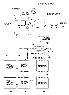
Fig. 1 shows an embodiment in block form of a feed-forward
amplifier in accordance with the present invention.
As shown in Fig. 1, the feed-forward amplifier is roughly
5 comprised of a divider 1, a vector adjuster 2, a main amplifier
3, a directional coupler 4, delay means 5, a directional coupler
6, a directional coupler 7, a pilot oscillator 8, delay means 9,
a directional coupler 10, a vector adjuster 11, an auxiliary
amplifier 12, a directional coupler 13, a directional coupler 14,
10 a detector 15, a detector 16, a temperature sensor 17, a control
circuit 18, a temperature sensor 19, a control circuit 20, a
nonvolatile memory 21 and a nonvolatile memory 22.
The divider 1 divides an input signal into two signal
components . The vector adjuster 2 adjusts the amplitude and phase
15 of a signal component from one of the output paths of the divider
1 in response to a control signal . The main amplifier 3 amplifiers
the output signal of the vector adjuster 2. The directional
coupler 4 couples a pilot signal to the output path of the main
amplifier 3. The delay means 5, e.g., a delay line, delays a
20 signal component from the other output path of the divider 1 . The
directional coupler 6 branches the signal from the output path
of the directional coupler 4. The directional coupler 7 couples
the signal extracted by the directional coupler 6 to the output
path of the delay means 5.
The pilot oscillator 8 generates the pilot signal . The delay
CA 02274996 1999-06-15
21
means 9, e.g., a delay line, delays the signal from the output
path of the directional coupler 6. The directional coupler 10
couples an output signal of the auxiliary amplifier 12 to the
output path of the delay means 9. The vector adjuster 11 adjusts
the output signal of the directional coupler 7 in amplitude and
phase. The auxiliary amplifier 12 amplifies the output signal
of the vector adjuster 11. The directional coupler 13 branches
the signal on the output path of the auxiliary amplifier. The
directional coupler 14 branches the signal on the output path of
the directional coupler 10. The detector 15 detects the strength
of the output signal of the auxiliary amplifier 12 through the
output of the directional coupler 13.
The detector 16, e.g., a synchronous detection circuit,
detects the strength (level) of the pilot signal component in the
output signal of the main amplifier 3 through the output of the
directional coupler 14. The temperature sensor 17 measures the
temperature in the vicinity of the main amplifier 3. The control
circuit 18 determines the passage loss and phase shift amount of
the vector adjuster 2 on the basis of both the value detected by
the detection circuit 15 and the temperature measured by the
temperature sensor 17. The temperature sensor 19 measures the
temperature in the vicinity of the auxiliary amplifier 12.
The control circuit 20 determines the passage loss and phase
shift amount of the vector adjuster 11 on the basis of the value
detected by the detection circuit 16 and the temperature measured
CA 02274996 1999-06-15
22
by the temperature sensor 19. The nonvolatile memory 21 stores
control values of the control circuit 18 corresponding to
temperatures measured by the temperature sensor 17. The
nonvolatile memory 22 stores control values of the control circuit
20 corresponding to temperatures measured by the temperature
sensor 19.
Next, the operation of the feed-forward amplifier of this
embodiment will be described with reference to Fig. 1.
An input signal is divided into two signal components by the
divider 1. The amplitude and phase of one of the two signal
components are adjusted by the vector adjuster 2, and the
resultant signal component is thereafter applied to the main
amplifier 3 to be amplified. The output signal is applied from
the main amplifier 3 via the delay means 9 and, at the same time,
part of it is extracted by the directional coupler 6.
The other signal component divided by the divider 1 is
appropriately delayed by the delay means 5, and the resultant
signal component is combined through the directional coupler 7
with the signal extracted from the output signal of the main
amplifier 3. The attenuation amount and phase shift amount of
the vector adjuster 2 are adjusted so that the transfer function
of a path from the input terminal to the directional coupler 7
via the main amplifier 3 and the transfer function of a path from
the input terminal to the directional coupler 7 via the delay means
5 are equal in amplitude but anti (reversed) -phase relative to each
CA 02274996 1999-06-15
23
other. Therefore, in the output of the directional coupler 7,
the main signal components (i.e., the signal components
equivalent in quality to the input signal having no distortions
added thereto) cancel each other, and hence only an error
component is output. The amplitude and phase of this error
component are adjusted by the vector adjuster 11, and the
resultant error component is thereafter amplified by the
auxiliary amplifier 12. In the output path of the auxiliary
amplifier 12 the strength of the output signal of the auxiliary
amplifier 12 is detected by the directional coupler 13 and the
detector 15. The control circuit 18 determines the passage loss
and phase shift amount of the vector adjuster 2 on the basis of
the value detected by the detector 15 and the temperature measured
in the vicinity of the main amplifier 3 by the temperature sensor
17.
The pilot oscillator 8 applies the pilot signal to the output
signal of the main amplifier 3 via the directional coupler 4, and
the delay means 9 appropriately delays the resultant output signal .
The delayed output signal is thereafter combined with the output
signal of the auxiliary amplifier 12 through the directional
coupler 10. The attenuation amount and phase shift amount of the
vector adjuster 11 are adjusted so that the transfer function of
a path from the main amplifier 3 to the output terminal via the
delay means 9 and the transfer function of a path from the main
amplifier 3 to the output terminal via the auxiliary amplifier
CA 02274996 1999-06-15
24
12 are equal in terms of amplitude but bear an anti-phase
relationship to each other. Therefore, an error component
(composed of signal distortion and noise) produced along the
transfer path via the main amplifier 3 does not appear at the output
terminal. Likewise, the pilot signal injected from the
directional coupler 4 is present only on the transfer path via
the main amplifier 3 in a manner similar to the error component.
Thus, if a distortion compensation is properly made, the pilot
signal does not leak at the output terminal. After the distortion
compensation has been made by the directional coupler 10, the
directional coupler 14 and the detector 16 detect the strength
of the pilot signal component in the output signal. The control
circuit 20 determines the passage loss and phase shift amount of
the vector adjuster 11 on the basis of the value detected by the
detector 16 and the temperature measured in the vicinity of the
auxiliary amplifier 12 by the temperature sensor 19.
Next, a technique for setting the passage losses and phase
shift amounts of the vector adjusters in the feed-forward
amplifier of this embodiment will be described.
In the feed-forward amplifier of this embodiment, control
values at the time of its activation are determined by
temperatures. More specifically, the temperature in the
vicinity of the main amplifier 3 is detected by the temperature
sensor 17, and the control value for the vector adjuster 2
corresponding to the detected temperature is determined by
CA 02274996 1999-06-15
referring to the value stored in the nonvolatile memory 21, and
the temperature in the vicinity of the auxiliary amplifier 12 is
detected by the temperature sensor 19, and the control value for
the vector adjuster 11 corresponding to the detected temperature
5 is determined by referring to the value stored in the nonvolatile
memory 22. Control values corresponding to temperatures are
previously written to the nonvolatile memories 21 and 22.
The control values during normal operations are controlled
by a similar technique to those disclosed by, e.g., the
10 aforementioned second and third prior arts. The transfer
function of the vector adjuster 2 is given by the control circuit
18 in such a manner that the detector 15 detects the strength of
part of the output signal of the auxiliary amplifier 12 extracted
by the directional coupler 13 and that the circuit 18 controls
15 the detected strength of that signal from the auxiliary amplifier
12 so as to be minimal. The transfer function of the vector
adjuster 11 is given by the control circuit 20 in such a manner
that the detector 16 detects the strength of the output signal
component of the pilot oscillator 8 injected via the directional
20 coupler 4 from the distortion-free output signal extracted by the
directional coupler 14 and that the circuit 20 controls the
detected strength of the distortion-free pilot signal so as to
be minimal . The pilot signal injected via the directional coupler
4 is present only on the transfer path via the main amplifier 3
25 in a manner similar to the distortion component. Therefore, if
CA 02274996 1999-06-15
26
a distortion compensation is properly made, the pilot signal does
not leak at the output terminal. Thus, by utilizing this
characteristic, the strength of the pilot signal is measured by
the detector 16 via the directional coupler 14 from the output
terminal, and the vector adjuster 11 is adjusted by the control
circuit 20 so that the strength of the pilot signal is minimized.
It should be noted that the level of the pilot signal injected
through the directional coupler 4 must be smaller than that of
the error component of the main amplifier 3 so as not to adversely
affect the detector 15 in its detecting the error component.
Here, a technique for writing the temperature-versus-
control-value data to the nonvolatile memories will be described.
The simplest technique for setting the control values of the
vector adjusters is to optimize the control values by artificially
changing the transfer functions of the vector adjuster 2 and those
of the vector adjuster 11. If temperature characteristics are
to be considered as disclosed by the fourth prior art, the control
values may be optimized for each temperature by changing the
temperatures around the amplifiers. However, this is not
productive, and hence elevates the manufacturing cost. On the
other hand, also available is a technique in which the optimal
control value is found for a specific temperature by hypothesizing
standard temperature characteristics and the control value
corresponding to a temperature change may be calculated from that
optimal control value . A simple technique to achieve this is to
CA 02274996 1999-06-15
27
change the control value in function of a temperature change using
a linear function. However, this technique addresses a
shortcoming that the total characteristics are impaired due to
a change in the error detection loop and error elimination loop
characteristics when there are deviations in the temperature-
versus-gain-change characteristics and temperature-versus-
phase-change characteristics of the amplifiers used.
As described above, the feed-forward amplifier of the
present invention provides means for implementing optimal
transfer functions corresponding to the temperatures at the time
of its activation and an automatic control mechanism for optimally
controlling the distortion characteristics during the actual
operations. As a result of this structure, a table of
temperatures versus control values can be prepared extremely
easily.
First of all, as a first technique, a regular signal is
applied to the feed-forward amplifier to carry out automatic
control in the aforementioned steady state, and when the
temperature characteristics become satisfactory under the
automatic control, a control value is written to the nonvolatile
memory 21 by referring to the value detected by the temperature
sensor 17, and a control value is written to the nonvolatile memory
22 by referring to the value detected by the temperature sensor
19. As a result of this operation, a table of temperatures versus
optimal control values can be obtained with ease.
CA 02274996 1999-06-15
28
Next, as a second technique, a regular signal is applied to
the feed-forward amplifier to carry out automatic control in the
aforementioned steady state while performing such a mild
temperature cycle as to allow the automatic control to follow and
the feed-forward amplifier to maintain the thermal equilibrium.
While keeping the distortion characteristics satisfactory under
the automatic control, a control value is written to the
nonvolatile memory 21 by referring to the value detected by the
temperature sensor 17, and a control value is written to the
nonvolatile memory 22 by referring to the value detected by the
temperature sensor 19. As a result of this operation, a table
of temperatures versus optimal control values can be prepared with
ease.
Further, as a third technique, a control value is written
to the first nonvolatile memory 21 by referring to the value
detected by the first temperature sensor 17, and a control value
is written to the second nonvolatile memory 22 by referring to
the value detected by the second temperature sensor 19 during the
actual operations with distortion characteristics maintained
satisfactory. As a result of this operation, a table of
temperatures versus optimal control values can be updated with
ease in accordance with long term fluctuations.
While the embodiment of the present invention has been
described in detail on the basis of the drawings in the foregoing,
specific structures of the present invention are not limited to
CA 02274996 1999-06-15
29
this embodiment, and therefore, the present invention includes
such design modifications and variations as not to depart from
the scope of its novel concepts. For example, the input signal
to the feed-forward amplifier of the present invention may be a
single-frequency signal or a mufti-frequency signal. Further,
the nonvolatile memories 21 and 22 may be constructed of EEPROMs .
As described above, according to the present invention, the
transfer functions immediately after the activation of the
feed-forward amplifier are determined immediately after the
activation by utilizing a previously prepared table of
temperatures versus control values. Therefore, a feed-forward
amplifier having satisfactory linearity characteristics
immediately after its activation can be constructed.
Further, the table of temperatures versus control values of
the feed-forward amplifier can be prepared automatically.
Therefore, a highly productive feed-forward amplifier can be
constructed.
Still further, the table of temperatures versus control
values can be updated automatically during the operation of the
feed-forward amplifier. Therefore, long term fluctuations of
the amplifier characteristics can be corrected, and hence a
feed-forward amplifier exhibiting less long term fluctuations of
its characteristics can be implemented.