Note: Descriptions are shown in the official language in which they were submitted.
CA 02275632 1999-06-18
WO 98127596 PCT/SE97102178
HIGH DENSITY ELECTRICAL CONNECTORS
TECFI~TICAL FIELD OF TfiE INVENTION
The present invention relates to interconnection of electric
devices, more particular to self-aligned) flexible high density
and impedance adjusted electrical connectors.
DESCRIPTION OF RELATED ART
The technical evolution in the field or integrated circuits,
IC: s, has resulted in a demand for faster and more compact
systems. In many applications a compact structure combined with
a low weight is in itself a requirement. The technical evolution
l0 also tends towards more complex systems involving a greater and
greater number of components which need ~., communicate with each
other. T_n order for the new systems to meet the requirement of
quick access between different components, the length of the
paths between different components of the system must be kept
within certain limits.
when the complexity of a system grows, the length of the paths
between components also grows. In order not to exceed the
maximutr; usable distance between. such comuonents, these
components have been bull t smaller ar.d smaller and ti:e~,~ have
also been packed more and more densely. Thus) mufti-chip modules
have been developed, which makes a very dense packaging of
unencapsulated IC:s possible.
In face, the distance between different active components do not
become much larger than if the whole system had been integrated
' 25 on the same plane monolith. The maxima. distanc, deter-: fined by
the performance requirements, between components which need to
communicate with each other in a complex. syster~ becomes
unnecessarily large if only one plane of connected
chips~ccmDOnents can be used, since oTl~~ comooner_=s fir. the sar.:=
1 .,~ -,n°_ = °C~:~_~. ''~ ~ i,o
n a__ ~ n ca:: b re~ wit____. t__ r;:Gxir,:al d=stance .
CA 02275632 1999-06-18
WO 98/2759b PGTISE97/02178
2
Three dimensional constructions can be used to overcome this
problem. This means that the communication lines extending from
one component can not only reach components in the same plane
but also components in planes located above and underneath the
component can be directly accessed. This can be obtained in some
different manners: firstly, systems having modules connected to
a back plane; secondly, systems consisting of chips glued
together; thirdly, systems having vertical connections at the
side of a tower built of chips are in one sense three
dimensional. These three dimensional constructions do not solve
the problem with short paths between all components. This can
not be achieved when components are close in space and are
connected by long lines. This becomes obvious when two
components are connected according to the first of the methods
described above, e.g. connection of two centrally located
components on two different neighbouring multi-chip modules,
which are in their turn connected through a lateral path, a
short vertical path at the side of the chips, and then a final
lateral path on the other chip. If more than one pile of chips
is used, the second described method does not either make short
interconnection lines between adjacent chips possible. This is
easily realised if one considers the case of two chips located
next to each other, but on the top of each pile, which are to
communicate with each other.
As the complexity of electronic circuits increases there is a
growing demand on the density of in/out-connections having
properties not to deteriorate the performance, i.e. impedance
adjustment cr negligible inductance/capacitance. As the density
increases t'.~.~ demand on alignment is also increased and the
create= this demand the more important becomes the use oz sel=-
CA 02275632 1999-06-18
WO 98!27596 PCTISE9710Z178
3
aligning procedures due to the accelerating costs of active
alignment at high precision.
When connecting parts of a complex system, the risk of having to
replace one or more of these parts to obtain a functioning
system increases with the complexity of the system. The
difficulty accelerates to fully test the constituent parts at
relevant frequencies and operating conditions.
There are concepts that use high density micro bumps, but these
are not really impedance controlled, which also implies quasi
impedance control.
The European patent application 0 295 914 A3, Maracos Karnezos,
describes elastic bumps which are metallized. The bumps are used
to connect two surfaces electrically through clamp connection.
Through the elasticity almost all thermal induced mechanical
stress can be eliminated. Conducting surfaces can be separated
without disordering.
SLT~ff~iARY
This invention describes a technology to achieve elastic
electrical connectors which are impedance controlled, have high
density of interconnects and are high precision self-aligned
during mounting and under performance. The functions of
alignment and electrical interconnect are in the same structure.
The alignment is based on protruding V-shaped bumps in one part
and V-grooves in the other part. The groove may be of 5 corner
pentahedron or pyramidical form and the bump may be of
. truncated 5 corner pentahedron or truncated pyramidical form.
The bumps and grooves have corresponding connector paths.
CA 02275632 1999-06-18
WO 98127596 PCT/SE97l02178
4
The basic idea with this invention is that it is using the
alignment of the structure itself. This means that the site of
multiple contact points may be obtained by high impedance
controlled contact densities, while the aligning structure is
relatively much larger. This results in high precision and at
the same time elastic connections. This invention handles minor
imperfections in the metal or other layers and possible thermal
mismatch when in use. Simultaneous multiple, more than three,
connections require individual contact point flexibility or
deformability or else, the demand on precision, i.e. the
requirement that all the contact points be ir. the same plane,
will be enormous and hardly realisable.
This invention has a mufti-path impedance controlled very high
density bus, made by patterning metal lines, e.g. paths, on a
precision moulded elastic bump which mates to similarly
patterned lines on the walls of a precision etched groove.
This invention is able to obtain impedance adjusted high density
mufti-path connectors at no physical fan out using low cost
lithography and Si micro structure technology. It is also a
self-aligning concept requiring no separate body and made
essentially simultaneously with the patterning of the metal
interconnects on the substrate utilising a pre-made change of
the structure of the substrates.
This invention could be used in various microelectronic systems,
for instance miniature high density modules, between modules and
motherboards, between IC:s and modules or boards, between
different levels in 3D structures, or generally as a very high
density dismountable connection between substrates.
CA 02275632 1999-06-18
WO 98/27596 PCT/SE97I02178
In many cases there is a requirement to be able to disassemble
electronic systems and to put them back again without using
soldering or equivalent. This implies using connectors. There
are numerous connectors available, but none that has the density
5 corresponding to this one, which is both impedance controlled,
for frequencies up to several GHz, as well as very high density,
i.e. without requiring physical fan out. The elasticity is an
important feature securing sufficient contact pressure for all
paths even if there are slight physical defects or variation in
size due to different thermal or other expansions. Regarding
alignment, many connectors utilise the contact points for
alignment. For very small sizes of the individual contact
points, this would require a high degree of pre-alignment or
might lead to destruction when forcing alignment. Instead,
elastic alignment structures and corresponding mating grooves
are patterned with similar metal lines which are part of the
metal lines extending from the circuit. This implies that a
robust alignment yet at very high precision is obtained, and
which does not occupy extra space. By making ground paths or
planes and contact paths in the grooves and also make similar
ground paths on the substrate and contact paths on the bumps it
will result in an connector structure. With the exception of the
formation of the bump and the groove, which requires simple
extra steps, the contact points and the connection of the
electrical lines are integral to the general interconnect
patterning processes.
One advantage of the present invention is that it offers a
solution for systems where very short electrical pathways are
reauired.
CA 02275632 1999-06-18
WO 98/27596 PCTISE97I02178
6
Another advantage of the present invention is that it offers a
compact packaging system.
A further advantage of the present invention is that the hole
system is easy to repair and, because of that, individual parts
are easy to replace and it could be done without any real costs
or potential damages associated with the removal of faulty
parts. An attachment does not involve soldering or gluing etc.
The invention is now being described further with the help of
the detailed description of the preferred embodiments and the
attached drawings.
BRIEF DESCRIPTION OF THE DRAWINGS
Figure 1 shows a cross-section of a three dimensional multi-chip
module.
Figure 2 shows a schematic cross-section of self-aligned and
impedance adjusted connector.
Figure 3 shows an alternative schematic cross-section of self-
aligned and impedance adjusted connector with double density
conductors.
4 shows an alternative schematic cross-section of self-aligned
and impedance adjusted connector with ground paths following the
signal paths through the connector.
Figure 5 shows a schematic top view of the Fig. 3.
Figures 6a-b show a cross section of an alternative connector.
Figure 7 shows a cross-section of an alternative double density
connector with conductors.
DETAILED DESCRIPTION OF EI~ODIMENTS
This invention can be used in various micro-electronic systems,
which are used for elastic electrical contacts and built-in chip
alignment. __ could ':~ used -n mul~=-chip mcdules, especia__v.~
CA 02275632 1999-06-18
WO 98/27596 PCT/SE97102178
7
where it is hard to determine the quality of chips before they
are mounted. The invention would be used where there presently
are several problems, e.g. with flip-chip or on board due to
high mis-match of thermal expansion coefficients between board
and chip. Repair can often be risky and expensive and, in some
types of MCM, essentially impossible.
First figure shows an example where this invention can be used,
but it is not restricted to this area. This invention can of
course be used in any kind of micro or even sub-micro systems .
Figure 1 shows a cross section for a three dimensional, 3D,
multi-chip module 100. The 3D module is formed by two
dimensional, 2D, multi-chip modules consisting of Si substrates
106-114 having integrated circuit chips 122-136 mounted thereon.
The Si substrates 106-114 are provided with a grounded plane
whereby a good screening is obtained between the different
planes of the module as well as for the entire 3D multi-chip
module 100. On the substrate 106-114, in particular the ones not
located at the top 106 or the bottom 114 of the stack of two
dimensiona~, 2D, multi-chip modules, there are also mounted
passive chips, via chips or vias 116-121 constituting
interconnections between adjacent levels of the 3D multi-chip
module 100.
In order to obtain impedance matched connectors, see Fig. 2, V-
groove etched contact grooves 202 are used. On the top of the
via chips 116-121 elastic bump structures 206 are applied and on
the backsides of the substrates V-shaped contact grooves 202 are
made, which are provided for obtaining a connection which is
easy to assemble/disassemble and for obtaining a good alignment,
see simultaneously filed patent application "Packaging structure
o; i ~earated circuits" .
CA 02275632 1999-06-18
WO 98127596 PCTlSE97102178
8
The IC chips 122-136 and the via chips 116-121 are, in the
preferred embodiment, flip-chip mounted on the substrates 106-
114. This arrangement makes it possible to provide a good
thermal contact between the backsides of the flip-chip mounted
IC chips 122-136 and the backside of the adjacent substrates
106-114.
Each level of the IC chip 122-136 and each individual via chip
116-121 of the 3D mufti-chip module 100 is only kept together by
a compressing force 142 applied on top plane 138 of the top
cooler 102 and bottom plane 140 of the bottom cooler 104 of the
structure.
In order to accomplish this piled structure, elastic bumps are
provided which connect via chips 116-121 to adjacent planes of
the substrates 106-114, and contact is obtained by pressing the
module together at the top plane 138 and the bottom plane 140 of
the cooler 102, 104. The compressing force 142 is provided by
means of clamps applied to the outermost part of the module 100.
Patterned metal layers are used to establish multiple electrical
pressure type, non permanent, connections which are impedance
adjusted for high speed data transmission.
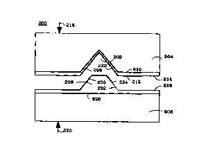
Figure 2 shows a cross-section of one such connector structure
200. A first part 204 consists of two metal layer structures, a
first signal path 212 and a first ground path or plane 210 with
a dielectric between them, covering the anisotropically etched
V-groove 202. A second part 208 consists of corresponding metal
layers, a second ground plane 226, and a second signal path 224
covering the elastic bump 205, which fits into the V-groove 202.
The first and th°_ seco_~.~, signal path 212 and 224 are in
contact
'.
471t:! ~aCn Ot~''_°_r When -~-' ~==sand the Second part 2~ = aWd 2~G
CA 02275632 1999-06-18
WO 98127596 PCT/SE97/02178
9
are brought together. The contact is self aligned 'when put
together, see a simultaneously filed patent application "Bumps
in grooves for elastic positioning". Because of the elastic bump
206, electrical contact will remain even if displacement due to,
for example, the thermal expansion occurs. The first and the
second signal paths 212, 224, configured as in Fig. 2 implies
double safety since both side walls of the elastic bump 206 and
the V-groove 202, respectively, are covered with the same paths.
In other words, if large displacement occurs and only one side
wall of the bump 206 is touching the V-groove 202, then
electrical contact will still remain. The first and the second
ground paths or planes 210, 226 consist of any suitable metal.
The first signal path metal 212 needs to be a metal free from
any insulating surface oxide layer, i.e. any noble metal. The
second signal path metal 224 needs to be a ductile metal free
from any insulating surface oxide layer, e.g. gold. The paths
and ground metal layers are separated by dielectric layers 214
and 216. The first dielectric layer 214 consist of any
dielectric layer conformally covering the V-groove walls, e.g.
Parylene. The second dielectric layer 224 consist of any
dielectric layer, or of the same elastic material as in the bump
206.
This invention is based on high precision, elastic alignment of
two parts of any function, where elastic bumps are
simultaneously used for high precision alignment and flexible,
elastic, electrical connectors. Patterned metal layers are used
to establish multiple electrical pressure type, non permanent
connections. These connections are impedance adjusted for high
speed data transmission.
CA 02275632 1999-06-18
WO 98/27596 PCT/SE97I02178
The most precise alignment will be obtained when the alignment
groove 202 is made using anisotropic etching of e.g. Si (100)
wafer. Likewise, the most perfect elastic bump 206 will be
formed by using: an anisotropically etched (100) Si wafer and
5 high precision lithography, a conformally covering release agent
layer, and a curable silicone compound. In simultaneously filed
patent applications "Method for making elastic bumps" and "Bumps
in grooves for elastic positioning" are described a more
detailed way how the bumps and the grooves are made and
10 alignment thereof. When the V-groove 202 and the truncated bump
206 have been made, parts will be placed by some pre-alignment
such that the top of the bump 206 is within the periphery of the
groove 202. By cautiously applying pressure 218) 220, possibly
gravity, inclined walls 230, 232 of the bump will slide on
inclined walls 222, 228 to get very precise alignment in the
directions parallel to a base surface of the bump 206 or the
groove 202 and then aligning the bump 206 in the groove 202. The
paths 212, 224 which were placed at high precision using
lithography relative to the bump 206 in the groove 202 are
2o automatically aligned and, utilising the elasticity of the bump
206, the paths 212, 224, will contact its counterpart regardless
of minute thickness, metal roughness due to micro
crystallisation etc., differences. Also, due to the elasticity,
small differences in expansion between the parts 204, 208 could
occur without losing contact or exposing the parts 204, 208 for
severe strain.
How to make the connector 200 is hereby described. A polished
(100) silicon wafer, this wafer is fror:, here on referred to as
the mould wafer, is covered using SiN after which resist is
deposited aTd patterned using a mas'.~ whic: is well aliened
rel alive tc t'_he crystGl axi s direc~ic~s c- z'_~_e moul d wa=e= .
CA 02275632 1999-06-18
WO 98/27596 PCT/SE97/02178
11
Openings as defined by the mask are then etched in the SiN
layer, then the mould wafer is exposed to an anisotrophic
etchant, which produces grooves which side walls are limited by
the silicon {111} planes. The etch may be continued until
complete, elongated, structure has been etched or preferably may
be stopped prior to this, such that truncated, elongated,
structure is formed.
A similar, but mirrored, mask which with very high precision,
rer~licates the first mask is then used to, by equivalent
procedure, obtain similar but mirrored grooves in a wafer which
contains th' parts which are to be aligned. These grooves must
be as deep or deeper than those in the first wafer . The mould
wafer may also contain some further alignment structures to
enable it to be self aligned to the substrate onto which the
elastic bumps are moulded. The mould wafer is covered with some
release agent, which is deposited very thinly and conformally in
order to preserve the precise geometry. For the part to be
provided with bumps the most rational procedure is to first
create the metal and dielectric layers as usual. Either the
plate with the unseparated substrates or the mould wafer is then
covered with a curable elastic compound to a controlled
thickness using spinning, scraping or spraying. Then the mould
wafer and the unseparated substrates are pressed using the
alignment features for precision alignment of the bumps versus
the substrate structures, allowing the compound to wet the
opposing s~.:rfaces. The package is then possibly placed in a
vacuum to remove air bubbles, and then at elevated temperature
to cure the compound. The mould wafer is then separated from the
substrate. Using stiff mould wafers and substrates this would be
no r ~tju:;, dale L:r th° ~':erm2L~C L °
3 0 do.__ i_. a va,. , it of th compound to tin
CA 02275632 1999-06-18
WO 98/27596 PCT/SE97102178
12
mould. For special applications the substrate could be made of
flexible material, which would facilitate separation.
For the bump structure part the most rational procedure is to
first create the metal layer 226 and the dielectric layer 214 as
S usual, then to make the bump, then a separate metal path 224 is
patterned over the bump and makes contact to the previous metal
layers through vias. It would, in principle, be possible to
first make the ground path or plane, then continue with the
depositions of metals and dielectric on the bump. This would,
however, exclude the possibility to pass lines or ground planes
beneath the bump and it is not always the case that the various
dielectric and metal paths would be flexible enough to survive
on the flexing bump.
By using photolithographic masking aligned to already existing
structures on e.g. lasers or IC:s or substrates before they have
been separated, grooves are made either using anisotropic
etching or other techniques. The grooved part 204 is then
processed normally, i.e. depositing the metal layer 210 and
dielectric layer 214, with the exception that tine dielectric
layers 214 and patterning the metal path 212 have to be
deposited conformally, in order to preserve the alignment
properties of the groove 202. Also, the resist has to be
deposited sufficiently conformally to allow resolution of the
exposed pattern in the resist and the depth of focus of the
exposing equipment must be sufficient.
After separation of the grooves etc. they may now be placed ontc
the bumped part, self-aligning grooves with the bumps. Depending
o.~. the shape and size of the bumps and the grooves the degree of
p=~-alignment varies.
CA 02275632 1999-06-18
WO 98127596 PCT/SE97102178
13
It would, in principle, be possible to first make the general
deposition and patterning of the dielectric layer and metal
path, then to etch away metal and dielectric from the area of
the groove, pattern and etch the groove, further to re-deposit
and pattern the metal path and the dielectric and resist, which
would only be used locally.
As the parts are mating together using external pressure no
permanent attachment is made, allowing the part to be easily
separated from its aligning structure for replacement or repair.
In the 'thin parts of the moulded material outside of the bump,
iT
vias are formed to the metal paths, which are to be contacted
very close to the bump.
In Figure 3 is a first alternative embodiment described. This
figure shows a possibility of having a double density connector.
The manufacturing process steps and materials involved are
identical with the case described in Fig. 2 However, in this
case shown in Fig. 3 there are two different paths on each side
of the bump as well as the grove. The paths pattern is also
illustrated in the schematic top view of a bus contact in Fig.
5.
A second alternative embodiment of the present invention is
described in Fig. 4. The manufacturing process steps and
materials involved are identical with the case described in Fig.
2 except that the ground plane is connected up to the level of
the signal lines using vias. Fig. 4 shows schematically a cross-
section of self aligned and impedance adjusted connector with
ground paths following the signal paths through the connector.
To achieve ultimate electrical performance both the signal line
CA 02275632 1999-06-18
WO 98/27596 PCTISE97102I78
14
and the ground plane are connected at essentially the same
position using the same elastic bump.
Figure S shows schematically a top view of, self aligned and
impedance adjusted connector with double density conductors'of
the alternative embodiment, Fig 3.
Figures 6a-b show a cross section of an alternative connector
600. The connector 600 having a first part 602 and a second part
604. The first part having signal paths 606 along the edge of
the part 602, see Fig. 6b, connected to contact pads 612 at
bottom of the first part. The second part 604 having a guiding
frame 610 on a substrate 614 and signal paths 608 along the
guiding frame 610. The two parts have such a structure that at
least one edge of each of the parts have inclined walls 616,
618. If chips are provided with inclined walls the normal pads
could be exchanged with paths extending over the inclined walls
and mating the guiding frame with patterned metal paths as
described earlier.
The previously described preferred embodiment could be modified,
but at some loss of precision. The bumps could have a different
shape than the grooves. For this, one would not use anisotrophic
etching, but rather some other etching, or machining. For this,
the grooves and the bumps do not have to have the same shape as
long as the bump would fit in the groove, in a self centring
fashion, and contacts were being made. The compound could be
other than Silicone, e.g. polyurethane or some other elastic or
semi-elastic compound.
By replicating using several steps) a flexible mould could be
made, faci?itating the detachment of the mould from the
substrate but only at a loss e. accuracy.
CA 02275632 1999-06-18
WO 98127596 PCTISE97/02178
Assuming that the metal patterning resolution is better than the
minimum size of the bumps the preferred embodiment gives the
highest contact density in one dimension) i.e. the closest
possible line spacing. If the minimum size of the bumps is
5 equivalent to the metal patterning resolution it would be
possible to obtain higher contact densities per area. In this
case self centring multiple super micro bumps densely packed on
a surface, where the metal is patterned not on the bump but
outside the bump would be used.
In this case the connections would also appear to be impedance
controlled due to the very small size of the bumps. This,
however, would be much harder to pre-align as the peak of the
bump must be within the perimeter of the now very small groove,
unless there are also some gross alignment features in the
structure.
If elastic material could be "perfectly" conformally deposited
on the walls of the groove a stiff bump could be used instead.
One way to accomplish this would probably be to use a mould,
which would fill part, but not all of the groove so as to leave
a thin distance to the groove walls where the elastic compound
would cure.
There are several possible applications for the present type of
connection. Bus contacts between MCM:s in the same plane, or
also vertical signal transmission between stacked MCM:s are
achievable) in combination with through-hole vias. In
combination with different fan out schemes as required, these
can be used as general fine pitch high frecruency connectors.
They would occupy much less space per connection than
cOIlvt''I:==.0:1 ~ el °r't= 1CS 1 ones , Vl:ll! ~ malT:4 ?.:llng .~_Or
r °C
CA 02275632 1999-06-18
WO 98/27596 PCTlSE97/02178
16
characteristic impedance. This is due to the fine pitch and high
alignment, and the fact that the ground plane is brought into
contact point.
Except for standard process technology for fabrication of
electronic devices, this connector device requires processes
such as a V-groove etching, casting of bumps, deposition of
conformal insulator coating, and lithography over large steps.
All these can be achieved by existing or modified
semiconductor/thin film processes.
In order to get maximum precision, there must be means to cover
the mould with releasing agents as very conformal and thin
layers. Methods for this were described above. For this maximum
precision case single crystals with surfaces well aligned to the
crystal directions that can be used for anisotrophic etching are
available as commercial Si-wafers.
The dielectric metal and resist layers are required to be
deposited relatively conformally, in comparison to the layer
thickness and topography of the groove and the bump. For the
metal layer deposition, this is normally the case using standard
thin film deposition techniques. For the dielectric, spin-
coating can most likely not be used, limiting the choice of
materials. However, there is still a number of materials and
processes to choose from, e.g. the Parylene method. The choice
of resist becomes more narrow as the vast majority of resists
are made to be deposited by spin-coating, which is not deemed
possible in this case. There are still two known alternatives.
One is using novel resist materials, which are deposited by
evaporation in vacuum. For this method there is no real
comc~ercial process available, but there exist commerciallw
aVG_1 ab! °_ m3=~rl~lS, ~~':llCi. na':°_ reSlSL
prOperL1°S and ca~: D.
CA 02275632 1999-06-18
WO 98127596 PCT/SE9710Z178
17
deposited this way. The other alternative is a type of resist,
which is electroplated. It is commercially available and
primarily used to protect the metal in through-plated holes on
printed circuit boards. These electroplated resists require that
there be a metal layer which can be biased for growth to occur,
which will be the case as the only layer that needs to be
patterned on the bumps and in the grooves are the metal layers.
The dielectric also needs to be patterned to get vias, however
this will not be on the bumps or in the grooves but rather
outside of these where more conventional resists can be used
provided they cover the hole or the groove to allow patterning,
even if they are too unevenly thick. It is also possible to
deposit and pattern a metal hard mask for patterning of the
dielectric.
Using micro machining technologies, very high density connectors
have been shown to create micro parts looking much the same as
conventional connectors, but being much smaller in size. These
are edge type connectors and can, in principle, be made so small
that they require no physical fan out of the line pattern.
However, they are not made as an integral part of the
metallization. Instead, they are separate parts that require
soldering or equivalent to be used. Little is known about their
robustness and wear resistance.
Elastic bumps have been shown to be used for single path
purposes. Here each path has one separate bump mating a surface
on the opposing substrate. In principle these could be made as
small as to not require physical fan out. In this case they
could also be regarded as impedance controlled. However, these
schemes lack any inherent means of alignment.
CA 02275632 1999-06-18
WO 98127596 PCT/SE97/02178
18
Solutions requiring separate micro parts that have to be
individually precision handled will never be very cheap compared
to thin film like processes where many items pre-placed are
produced with lithographic methods.
Figure 7 shows a cross section of an alternative connector bump
700. The connector bump consist of a two metal layer structure,
a dielectric medium 704 and a elastic structure 216. The metal
layer structure can be a ground path or plane 702 and a signal
path 706. The ground plane 702 is made on the bump 206 where the
l0 bump is including in the elastic structure 216. The ground plane
also has a connection through the dielectric medium 704 up over
and covering partly the dielectric medium 704. The other metal
layer structure, the signal path 706, is made on the dielectric
medium 704.
The invention described above may be embodied in yet another
specific forms without departing from the spirit or essential
characteristics thereof. Thus, the present embodiments are to be
considered in all. respects as illustrative and not restrictive,
the scope of the invention being indicated by the appended
claims rather than by the foregoing descriptions, and all
changes which come within the meaning and range of equivalency
of the claims are therefore intended to be embraced therein.