Note: Descriptions are shown in the official language in which they were submitted.
CA 02275640 1999-06-15
PATENT 1 M 1990-4
W:\USERS\LYMAMwpdataVvt 1990-4
MANUFACTURE METHOD FOR ,A MONOCRYSTAL AND
MONOCRYSTAL MANUFACTURING DEVICE
BACKGROUND OF THE INVENTION
This invention relates to a method and device for directly crystallizing a
monocrystal without using a seed crystal. This is achieved by first
supercooling
a melt of molten raw material which is floating under microgravitational
conditions, then generating a crystal nucleus, and solidifying the melt. This
invention relates to an art which is particularly suitable for the manufacture
of
granular monocrystals of single elememt semiconductors and granular
monocrystals of compound semiconductors.
Single element semiconductor crystals, such as silicon or germanium or
the like, two-element compound semiconductor crystals, such as GaAs, GaP,
GaSb, InAs, InP, InSb, ZnSe, CdTe, or the like, or mixed crystals in which 2
two-element compound semiconductors are mixed have been used as materials for
electronics devices. The quality of these semiconductor crystals has a large
effect
on device performance. As a result, the art of manufacturing high quality bulk
monocrystal (monocrystal), having few crystal defects and having a controlled
composition ratio of the component elements and impurity concentration
distribution, is extremely important.
If monocrystals can be manufactured by directly synthesizing a chemical
compound melt from the semiconductor raw material and directly solidifying
this
melt without using seed crystals, the performance of the electronics device
can be
improved. This is also preferable in terms of l:he manufacturing cost.
Presently,
CA 02275640 1999-06-15
PATENT 2 M 1990-4
W:\USERS\LYMAN\wpdataUv1I990-4
known methods in which large bulk monocrystals are grown by solidifying melt
of semiconductor raw material include CZ method, FZ method, Bridgemam
method, and the like.
However, with all of these methods, the: monocrystal is grown from a seed
crystal, and as a result, a good quality seed crystal must be prepared first.
Generally, the method which is adopted is a method in which the seed crystal
is
cut from a large monocrystal which is manufactured separately. However,
depending on the type of semiconductor, it can be difficult to manufacture a
good
quality monocrystal. In these cases, a sintered body or a precious metal rod
is used
as a seed, and a polycrystal is grown. A monoc~rystal portion with a
comparatively
large grain is cut from this polycrystal and malde into the seed crystal.
However,
it is difficult to obtain a good quality seed crystal.
In the method for growing crystals from a melt of the prior art, complex
fluid motion is generated within the melt due to the influence of gravity, and
it is
known that this can have a large effect on the quality of the growing crystal.
As
its most important drawback, a crucible for storing the melt is needed. A
reduction
in the purity of the crystal or defects in the crystal are generated because
of the
chemical physical actions of the crucible. Thermal convection is generated
when
there are temperature differences within the: melt. Because of the resulting
fluctuation in the temperature and composition at the solid/liquid interface,
crystal
defects are readily generated, and quality is unstable. This results in a
crystal with
non-uniform composition and many crystal defects.
In order to eliminate the negative effect of gravity, various experiments
have been conducted on growing crystals under microgravitational conditions
which are achieved in space stations, space: shuttles, rockets, and airerafts.
CA 02275640 1999-06-15
PATENT 3 M 1990-4
W:\USERS\LYMAMwpdataUN 1990-4
However, the costs for crystal manufacture becomes enormous, and the materials
which can be used become limited. In addition, because of minute gravitational
disturbances called G jitters, shaking is generating during the crystal growth
period. This is not ideal. Recently, a free-fall facility located on the
ground has
achieved microgravitational conditions with few G jitters, although only for
the
short period of time of approximately 10 seconds. There is much anticipation
on
its use, but methods for directly growing monocrystals from melts have not
been
proposed.
For example, in US Patent number 4,021,323, there is described a
technology, wherein: molten silicon droplet is shot from a small nozzle which
is
placed on the upper end of a shot tower; silicon melt is allowed to free fall
in air
from the shot tower, and granular crystals of silicon are created. However
with
this technology, an adequate microgravitationa.l environment is not created
due to
the air resistance during the fall. In addition, impurities from the nozzle
may
become dissolved into the molten silicon.
The present invention is based on new facts discovered by the present
inventors while conducting various experiments of creating spherical crystals
from
semiconductor melt under microgravitational conditions generated by a free
fall
facility.
OBJECTS AND SUMMARY OF THE IN'~ENTION
The obj ect of the present invention is the following: to provide technology
for manufacturing monocrystals from melts of various semiconductor materials
(single element semiconductors, a plurality of types of single element
CA 02275640 2002-10-17
semiconductors, compound semiconductors) without using seed crystals; to
provide
technology for manufa.eturing kvgh quality monocrystals with few crystal
defects; to provide
technology for manufacturing monocrystals from melts Qf various other
materials without
using seed crystals; and the Like.
According to opt aspect of the present invention, there is provided a method
of
making a monocrystal comprising. heating a raw material to at least its
melting point to form
a molten nnass; reducing a temperature of said molten mass, thereby forming a
supercooled
molten r~taass; reducing surface energy of at least a portion ofa surface of
said supercooled
molten mass, while levitating said supercooled molten mass under
microgravitational
1o conditions, thereby forming a crystal nucleus; and solidifyix~ said
supercooled molten mass
having said crystal nucleus under microgravitational car~ditioras to form a
granular
mofi~OGt'ySta~.
According to preferred embodiments of the invention, while being ievitxtod
under
microgravitational conditions of a gravitational acceleration o~ approximately
10''to 10'' G,
15 the melt, where raw material such as a semiconductor has bten melted,
becomes a spherical
malt in which the action of surface tension maintains a free surface. While
maintaining
levitation, the tempCraturc is lowered, and it is superroolod. Because it is
being levitated
undtr microgravitational conditions and without contact, there is no non-
uniform nucleus
generation. Because thtre is little variation in the temperature or density
within the milt, the
2 0 free energy barrier to uniform nucleus generation is high, and the degree
of supercooling
btcomes high. A crystal nucleus is generated by lowering the surface free
energy of a potion
ofthis spherical melt which has been supercooled tQ a high degree. With this
generation of
2S
34
the crystal nucleus, the supercooled spherical melt r8riidlv qnlidifiea infn a
CA 02275640 1999-06-15
PATENT 5 M 1990-4
W:\USERS\LYMAMwpdata\M1990-4
granular monocrystal. In order to lower the surface free energy of a portion
of the
surface of the spherical melt, a highly chemically stable solid, which is to
become
the site of nucleus generation, can contact one end of the surface of the
spherical
melt for a short period of time, for example. 'JVhen this method was
experimented
with semiconductors such as germanium (<ie), gallium antimonide (GaSb),
indium antimonide (InSb), or the like, it was possible to manufacture granular
monocrystals which were solidified spherical melts. In this manner, various
single
element semiconductor materials can be used for the raw material, and various
compound semiconductor materials can also be used. When the raw material is
a multi-element semiconductor compound which has a composition of 3 elements
or greater, the raw material can be a polycrystal which has the stoichiometric
composition of the compound, or the raw material can comprise the
semiconductor material which already has each of the component elements
weighed and mixed in the stoichiometric composition. However, this method is
not limited to monocrystals of semiconductors, and monocrystals of various
metal
materials and various insulating materials cam also be manufactured. It is not
completely understood scientifically how it is possible to grow monocrystals
with
this method. When a spherical melt is under microgravitational conditions and
is
not in contact with other substances and becomes spherical due only to the
force
of surface tension and reaches a supercoole~d state where free energy is at a
minimum, although the configuration of the spherical melt is a loose bonding
between atoms, there is believed to be a regularity in the atomic alignment
similar
to that of a solid monocrystal. Because of this, iit can be hypothesized that
with the
generation of a crystal nucleus, a rapid monoc:rystal growth is initiated.
CA 02275640 2002-10-17
When the raw mAttrial includes a semiconductor material with a high vapor
pressure,
it is prerferable to conduct steps I..4 while housing the raw materials within
a capsule. In this
situation, tht semiconductor materials other than the semiconductor with the
high vapor
pressure can be housed in advance in the main compartment of the capsule; the
s semiconductor material with the high vapor pressure cars be haustd in
advance in an auxiliary
compartment which connects with the main compartment ofthc capsule; and in the
first step,
it is possibly to heat the semiconductor material inside the main compartment
and the
semiconductor material inside the auxiliary compartment to different
temperatures. It is
preferable to conduct steps t-4 under one of the following environments:
vacuum
environment, inert gas environment, axidizang gas environment. Furthermore, by
irradiating
an ion beam for a short period of limo at a portion oftho surface of the
superGOOted spherical
melt, surface frte energy can be towered.
By the method of making manacrystals of the present invention, moaocrystals
can be
manufactured from the meh of various single element sernicanductor materials
without using
~.5 a seed crystal. Without using lead crystals, monocrystals of compound
semiconductors can
be manufactured from the melt of a plurality of types of single element
semiconductor
materials ar from the melt of cornpound senuconductor materials. Monocrystals
can be
manufactured from the melts of various materials without using seed crystals
by using a
simple method which makes use of a microgravitational environment.
z o According to a second aspect of the invention, there is provided a device
for
manufacturing a monocrystal from a mw material comprising; a chamber case
forming an air-
tight chamber; means for achierring rnicrogravitational canditians in said
chambeir case; a raw
material container located in said air-tight chamber staring said raw
material; means for
heating said raw material inside said raw material container; and an actuator
supporting said
2 5 raw material container in said chamber case, said actuator for moving said
raw material
container with respect to said chamber case.
In preferred embodiments of this second aspect of the presort invention, the
raw
material inside the raw material container is heated and melted by the heating
means. Inside
the raw material~comainer, while being levitated without contact under
microgravitational
3 o conditions, the meat is cooled to a supercooled spherical melt. While
being levitated without
contact under microgravitational conditions, the raw material container is
moved with respect
CA 02275640 2002-10-17
7
to the chamber case by the actuator. As a result, a portion of the surface of
the suporcooied
spherical melt contacts the solid surface of the raw material cantainer, and a
crystal nucleus
is generated in the spherical melt. The spherical melt is solidified, and a
granular rtvonocrystal
is rraanufactured.
The heating means can have a construction, comprising: an ellipsoidal
reflective
surface; and a halogen lamp which is placed at the focal point of this
ellipsoidal reflective
surface. The monocrystat manufacturing device of the present invention is a
monocrystal
mxrmfacturing device which can be used with a variety of means for achieving
microgravitational conditions. A monocrystal manufacturing device with a
simple
1o constructions is provided. Otherwise, all the same advantages as the
monocrystaJ
manufacturing method is exhibited.
According to a third aspect of the present invention, thore is provided a
device for
. manufacturing a monocrystal from a raw material comprising: an air-tight
drop tube,
extending vertically; retaining means to hold said raw material at x top of
said drop tube;
releasing means to release said raw material from said retaining means;
heating means for
heating and melting said raw material retained by said retaining means to form
a molten mass;
crystal nucleus generating means to generate a crystal nucleus in said molten
mass while said
molten mass is retained under said microgravitational conditions; said crystal
nucleus
generating means lawcring a free energy of a portion of a surface of said
molten mass during
2 o free fall of said molten mass along said drop tuba after said molten mass
is supercaoled while
free falling inside Bawd drop tube; and a recovery pa~~ said recovery part
recovering said
manoarystal formed fraxx~, solidification of said molten mass uain~ said
crystal nucleus as a
nucleus.
There is a suctioning means which suctions the air inside the drop tube and
makes a
2 3 vacuum. The spherical melt drops in a vacuum inside the drop tube. The
heating means can
have a construction comprising; an ellipsoidal reflective surface; and a
halogen lamp located
at the focal point ofthis ellipsoidal reflective,surface. The crystal nucleus
generating means
can have a construction of a rotating plate of a highly chemically stable
solid material which
is placed in the falling pathway of the spherical melt inside the drop tube.
According to this
3 o monocrystal manufacturing device, microgravitational conditions era
achieved by free fall,
CA 02275640 2002-10-17
g
and therefore it is possible to have the device installed on the ground.
Otherwise, the same
advantages as the monocrystal manufacturing method are exhibited.
According to a fourth aspect of the present invention, there is provided a
device far
manufacturing x moc~ocrysts,l from a raw material comprising: a,n air-tight
drop tube
3 extending vertically; a capsule containing said raw material; retaining
means to bald said
capsule at a top of said drop tube; releasing means to release said capsule
from said retaining
means; heating moans to heat arid melt mid raw material into a molten mass
inside said
capsule while said capsule is held by said retaining means; crystal nucleus
generating moans
to generate a crystal nucleus in said molten mass, said crystal nucleus
generating means
lowering a free enargy of a portion of a surface of said molten mass during
free fall of said
molten mass inside said capsule along said drop tube after said molten mass
inside said
capsule is supercooled during its free fall inside said drop tube; and a
recovery part, Said
recovery part recovering said capsule and said monocrystal which, during free
fall, solidified
into a manocrystal using said crystal nucleus as a nucleus.
CA 02275640 1999-06-15
PATENT 9 M 1990-4
W:\USERS\LYMAMwpdata\M 1990-4
The raw material is heated and melted while :housed in the capsule. The melted
raw material is dropped together with the capsule. In this case, because the
spherical melt can not be contacted with a rotating plate of solid material
during
the fall, the crystal generating means is preferably a construction which
includes
means for deceleration which is placed in the fall pathway of the capsule
inside
the drop tube and which can decelerate the capsule during the fall.
According to this monocrystal manufacturing device, monocrystals of
compound semiconductors which contain semiconductor materials with a high
dissociation pressure can be manufactured without using seed crystals.
Otherwise,
the same advantages as the monocrystal manufacturing method are exhibited.
The above, and other objects, features and advantages of the present
invention will become apparent from the; following description read in
conjunction with the accompanying drawings, in which like reference numerals
designate the same elements.
BRIEF DESCRIPTION OF THE DRAWI:~1GS
Figure 1 is a longitudinal cross-section. of the monocrystal manufacturing
device of Embodiment 1.
Figure 2 is a longitudinal cross-section. of the monocrystal manufacturing
device of Embodiment 2.
Figure 3 is a longitudinal cross-section. of the monocrystal manufacturing
device of Embodiment 3.
Figure 4 is the longitudinal cross-section of the top portion of the
monocrystal manufacturing device of Figure :3.
CA 02275640 1999-06-15
PATENT 10 M 1990-4
W \USERSU.YMAI~wpdataUN 1990-4
Figure 5 is the longitudinal cross-section of the rest of the monocrystal
manufacturing device of Figure 3
Figure 6 (a)-(e) is an explanatory figure explaining, in 5 stages, the state
and behavior of the raw material inside the ampule when a monocrystal is
manufactured by the monocrystal manufacturing device of Figure 3.
DETAILED DESCRIPTION OF THE PREFERRED EMBODIMENTS
Embodiment 1 (refer to Figure l~
The monocrystal manufacturing device of the present embodiment is a
monocrystal manufacturing device suitable fer using with means for achieving
microgravitational conditions. The monocrysvtal manufacturing device, aided by
the microgravitational conditions achieved by the microgravity achieving
means,
manufactures monocrystals from raw materials.
The microgravity achievement means include: formats which achieve
microgravitational conditions by dropping objects, such as drop tubes, drop
towers, airplanes and small rockets, and formats which achieve
microgravitational
conditions by balancing the force of gravity with centripetal force in an
orbit, such
as space shuttles, free flyers, recovery capsules and space stations, or the
like.
Referring to Figure l, among the various microgravity achieving means,
this monocrystal manufacture device is suitable for use with a microgravity
achievement means which has comparatively few restrictions in terms of usage
space or usage time. This monocrystal manufacture device will be described
first.
Referring to Figure 1, there is a monocrystal device l, comprising: a
stainless steel chamber case 3, which is air tigl-~t and forms a chamber 2
which has
CA 02275640 1999-06-15
PATENT 11 M I 990-4
W:\USERS\LYMAMwpdataVv11990-4
a circular cross-section; a graphite raw material container 5, which is placed
inside
chamber 2 and stores raw material 4a; a stainless steel support rod 6, which
supports raw material container 5 onto charrcber case 3; a solenoid actuator
7,
which, via support rod 6, drives an up and down motion of raw material
container
5 relative to chamber case 3; a gold image furnace 8 as the heating means for
heating raw material 4a inside raw material container 5.
Raw material container 5 comprises: a tray Sa at the lower end for placing
raw material 4a; a plurality of support poles Sb; a ceiling Sc. Small rod 6a
on the
bottom of support rod 6 is fixed to a stainless steel holder 6b which is
connected
to ceiling Sc of material container 5. The 9 particulate raw materials 4a are
placed
on a plurality of concave areas Sd (there are 9 with a diameter 2.2 mm, depth
1.5
mm, and a length and breadth pitch of 3 mm) formed on tray Sa. A thermocouple
9 is attached to the bottom surface of tray Sa for temperature measurement.
Its
lead wire (not shown) extends along support pole Sb of material container 5,
1 S passes through a wire pathway inside support: rod 6, extends to the
outside, and
is connected to a control unit (not shown). Solenoid actuator 7 is constructed
so
that, by a solenoid coil, it can drive the up and down motion of support rod 6
at
a specified stroke (for example, approximately 2 mm). Solenoid actuator 7 is
controlled by the control unit.
Chamber case 3 comprises a cylindrical tube 3a and a top plate 3b which
closes the top end. On the side of tube 3a, an opening window (not shown)
which
observes raw material 4a is formed. In order t~o make the inside of chamber 2
an
inert gas (for example argon gas or the like) environment, tube 3a is provided
with
the following: a port 10 for exhausting air by a vacuum pump and for supplying
inert gas, an exhaust port 11 for allowing inert: gas to flow inside chamber
2, and
CA 02275640 1999-06-15
PATENT 12 M 1990-4
W:\USERS\LYMAN\wpJata\h11990-4
an closing valve 12 which can open and close discharge port 11. At least
during
the time when raw material 4a is being melted and solidified, the flow of
inert gas
is stopped, and air tight conditions can be maintained.
A transparent quartz plate 13, which has excellent light transparency,
creates a partition between chamber 2 and gold image furnace 8. There are O
rings
14 around the perimeter on both sides of duartz 13. Gold image furnace 8
comprises: a furnace body 16 of an aluminun>/magnesium alloy; a gold-plated,
ellipsoidal, reflective surface 17 which is formed on the inner surface of
furnace
body 16; a halogen lamp 18 (maximum power consumption of 1 kW), which has
its light emitting part positioned on the focal point of ellipsoidal
reflective surface
17; a fine adjustment mechanism for fine adjustments to the position of
halogen
lamp 18; a pathway formation 21, which forrr~s a cooling water pathway 20.
When electrical current is supplied from lamp terminal 22 of halogen lamp
18, infrared light, which radiates from the light-emitting part of halogen
lamp 18,
is reflected off of ellipsoidal reflective surface 17, passes through quartz
plate 13,
and converges onto the other focal point of ellipsoidal reflective surface 17.
Because tray Sa of raw material container 5 is positioned on the other focal
point,
raw material 4a inside raw material container 5 can be melted at the specified
temperature.
Furthermore, in monocrystal manufacturing device 1, raw material
container 5 and support rod 6 and solenoid actuator 7 correspond to the
crystal
nucleus generating means. However, an up/down driving actuator other than
solenoid actuator 7 can also be used.
Monocrystal manufacturing device 1 is placed inside a drop capsule which
is used for a drop shaft at the Underground :?ero gravity Experimental Center
CA 02275640 1999-06-15
PATENT 13 M 1990-4
W:\USERS\LYMAMwpdata\M 1990-4
(located in Hokkaido of Japan). Under microgravitational conditions
(maintained
for 10 seconds) of 10-4 G or lower which is .achieved when the drop capsule is
falling at the gravitational acceleration, the crystal growth experiment was
executed as follows. It was possible to directly grow a granular monocrystal
from
a spherical melt of semiconductor raw material without using a seed crystal.
First, each of a total of 9 particles of raw material 4a, which were cubic Ge
crystals with a purity of 9N and with a side of 1.47 mm, was housed on each of
the 9 concave areas Sd. Next, air was exhausted from inside chamber 2 to
create
a vacuum, and afterwards, as argon gas was flowing inside chamber 2, raw
material 4a was heated and melted by halo;;en lamp 18. For the temperature
setting of gold image furnace 8, the temperature at which there is complete
melting under a gravity of 1 G was confirmed by eye in advance, and the
temperature was set for 2-3 degrees C higher than this temperature.
Next, after raw material 4a was melted, closing valve 12 was closed, and
the inside of chamber 2 was made into a still environment of argon gas. After
maintaining the melting temperature for around 15 seconds, the fall of the
drop
capsule was initiated. After 1-3 seconds after the initiation of the fall, the
power
to halogen lamp 18 was shut off, and at the sarrre time, solenoid actuator 7
was
operated so that raw material container 5 was moved approximately 0.2 mm
downward (in the direction of the fall of the drop capsule) at a speed of
20mm/sec.
As a result, from concave area Sd of tray Sa, melt 4b floated upwards relative
to
raw material container 5, becoming a spherical melt. While cooling naturally,
it
entered a supercooled state. Due to inertial motion, within a few seconds,
spherical melt 4b collided with the solid surface of ceiling Sc or support
pole Sb
of raw material 5. By the contact with the solidl surface, the surface free
energy on
CA 02275640 1999-06-15
PATENT 14 M 1990-4
W:\USERSU.YMAMwpdata\M 1990-4
a portion of the surface of supercooled spherical melt 4b was lowered, and a
crystal nucleus was generated at a portion of spherical melt 4b. The behavior
of
melt 4b was recorded in real time with a video camera. Afterwards, during the
fall
of the drop capsule, melt 4b continued to radiate heat, and a crystal
continued to
grow and solidify from the crystal nucleus of spherical melt 4b, and this
resulted
in a granular monocrystal. After the 10 second , of microgravity environment
time
(the time during which the drop capsule is falling at the gravitational
acceleration), the drop capsule received a braking force by a brake and was
received and stopped at the bottom of the drop tower. Afterwards, monocrystal
manufacturing device 1 was removed from the drop capsule, and the monocrystal
was removed from monocrystal manufacturing device 1.
Some of the monocrystals had returned to the bottom of tray Sa after
contacting with a solid surface, and others remained adhered to the solid
surface.
On all of the monocrystals, there was evidence that they had contacted a solid
surface. The monocrystals in which the collision with the solid surface was
gentle
had a nearly spherical shape. The monocrystals which had a more severe
collision
with the solid surface had a projectile shape. However, in all of the
monocrystals,
when the crystal properties were examined wiith X ray analysis, a periodic
Laue
spot was observed, and they were confirmed as being monocrystals.
Referring to Figure 1, the changes witlh time of a typical raw material 4a
is shown. The unmelted raw material 4a is indicated on the right edge of tray
Sa,
and to the left of this, melt 4b, before it enters microgravitational
conditions, is
shown. As indicated underneath the ceiling surface, spherical melt 4b, after
it
enters microgravitational conditions, levitates, and, due to inertial motion,
contacts ceiling Sc of raw material container _'..
CA 02275640 1999-06-15
PATENT 15 M 1990-4
W:\USERS\LYMAMwpdata\M 1990-4
Other than the raw material of germanium (Ge), the same experiment was
conducted using the raw materials of gallium antimonide (GaSb) and indium
antimonide (InSb). For both of these, the raw materials which were used had
sizes
which were cut to 0.4 mm3. l -4 particles were stored in each of concave areas
Sd.
These were melted, and melts were made' for each. The heating melting
temperatures were set according to the raw material. The time until the raw
material 5 was lowered was in the range of 1-:p seconds after the initiation
of the
fall. The levitating time until the spherical melt contacted a surface was
within 2,
3 seconds. After the fall of the drop capsule was completed, the monocrystals
were collected and examined by X-ray analysis. They were confirmed to have
been monocrystallized.
In the manufacturing technology for tlhe monocrystal which is described
above, monocrystal manufacturing device 1 is used in a microgravity achieving
means. Monocrystal manufacturing device 1 solidifies spherical melt 4b, which
has been supercooled under microgravitational conditions, into a monocrystal.
With this monocrystal manufacture technology, various advantages are
achieved. There are few space and time restricaions needed in order to utilize
the
microgravitational conditions achieved by the microgravity achieving means,
and
various conditions for crystal growth can be s~>ecified. The technology is
suitable
for manufacturing monocrystals in the microg;ravitational environment of
space.
A granular monocrystal can be manufactured from the melt of a raw material
without a using seed crystal. Monocrystals of various materials (single
element
semiconductors, compound semiconductors, metal material, insulating material,
or the like) can be manufactured. A monocrystal can be manufactured with a
small
device.
CA 02275640 1999-06-15
PATENT 16 M 1990-4
W:\USERSU.,YMAMwpdata\M 1990-4
Embodiment 2 (refer to Figure 2~
The monocrystal manufacturing device of this embodiment is a device for
manufacturing monocrystals utilizing microgravitational conditions created by
free fall on the terrestrial surface. The method of manufacturing monocrystals
with this device is relatively easily implemented.
First, referring to Figure 2, this mono<;rystal manufacture device will be
described.
Referring to Figure 2, monocrystal manufacture device 31 comprises: a
chamber case 34, which forms a chamber 3?.; chamber 33, which houses raw
material 32a and creates a vacuum atmosphere; a gold image furnace 35, which
is placed as a heating means above chamber 33; an upper drop tube 36, which is
connected to the lower end of chamber case 34 and extends vertically to a
specified length (for example 4m); upper drop tube 36 allows for a
perpendicular
free fall of the spherical melt 32b which is the melted raw material 36a; a
lower
drop tube 37, which extends downward from the bottom of upper drop tube 36
and which has the drop length (for example 1 O~m) needed for the time required
to
solidify melt 32b; a raw material supply/retention mechanism 38 which supplies
raw material 32a to the inside of chamber 33 and retains raw material 32a so
that
it can be either retained or released; a graphite rotating piece 39, which is
installed
near the top of lower drop tube 37 and which contacts melt 32b for a short
period
of time during its fall; a recovery vat 40, which is connected to the bottom
of
lower drop tube 37 and which is equipped with a liquid vat which absorbs the
impact of the crystallized monocrystal and cools it.
Referring to the Figure, a transparent quartz plate 41 creates a partition
CA 02275640 1999-06-15
PATENT 17 M 1990-4
W:\USERS\LYMAN\wpJataU11990-4
between chamber case 34 and gold image furnace 35. An air lock 42 creates a
partition between chamber case 34 and upper drop tube 36. An air lock 43
creates
a partition between upper drop tube 36 and lower drop tube 37. When air lock
42
is opened, chamber 33 and the inside of upper drop tube 36 are in
communication.
When air lock 43 is opened, the inside of upper drop tube 36 and the inside of
lower drop tube 37 are in communication. Gold image furnace 35 has the same
construction as in Embodiment 1. An ellipsoidal reflective surface 45 is
formed
on the bottom surface of a furnace body 44. A halogen lamp 46 is installed at
the
focal point of ellipsoidal reflective surface 4:i. The infrared rays radiated
from
halogen lamp 46 converge onto the other focal point inside chamber 33. Raw
material 32a, which is retained by raw material supply/retention mechanism 38,
is placed at this lower focal point.
Raw material supply/retention mechanism 3 8 comprises: a quartz rotating
pole 47; a holding compartment 47a, which is formed on the left end of
rotating
pole 47 and retains raw material 32a; a quartz sleeve 48; a quartz raw
material
inserting pole 49; a pivoting actuator 50, which pivots rotating pole 47 180
degrees; a reciprocating actuator 51, which drives a reciprocating motion of
raw
material inserting pole 49; a raw material input opening 52, which is formed
on
sleeve 48; and the like. Rotating pole 47 is introduced into chamber 33 by
passing
through the right wall of chamber case 34. On the left end of rotating pole
47, a
holding tube, which has a circular cross section and is open on the left end,
is
formed. Inside the holding tube, a holding compartment 47a, which retains raw
material 32a, is formed. An opening 47b, which is for dropping melt 32b, is
formed on the top end of the holding tube.
Sleeve 48 is introduced into chamber 33 by passing through the left wall
CA 02275640 1999-06-15
PATENT 18 M 1990-4
W:\USERSU.YMAMwpdata\M 1990-4
of chamber case 34. The right end of sleeve 48 is fitted into the holding tube
and
can rotate freely. Raw material insertion pole 49 is inserted from the left
end of
sleeve 48 into sleeve 48. Raw material 32a, which is supplied to the inside of
sleeve 48 from raw material input opening 52, is pushed into holding
compartment 47a by raw material inserting pole 49. Raw material input opening
52 can be sealed by a cap 53 and an O ring. Thf: left end of sleeve 48 can be
sealed
air tight by a box nut 54 and an O ring.
In order to change the interior of chamber 33 into a vacuum or an inert gas
environment, chamber case 34 is equipped with an exhaust port 58 and a closing
valve 59 which can open or close exhaust port 58. A vacuum pump and an inert
gas supply device are connected to exhaust port 58 in a switchable format.
Similarly, in order to change the interior of upper drop tube 36 into a vacuum
or
an inert gas environment, upper drop tube 36 is equipped with an exhaust port
60
and a closing valve 61 which can open or close: exhaust port 60. A vacuum pump
and an inert gas supply device are connected to exhaust port 60 in a
switchable
format. Similarly, in order to change the interior of lower drop tube 37 and
recovery vat 40 into a vacuum or an inert gas f;nvironment, lower drop tube 37
is
equipped with an exhaust port 62 and a valve E.3 which can open or close
exhaust
port 62. A vacuum pump and an inert gas supply device are connected to exhaust
port 62 in a switchable format. Rotating plate :39 is installed so that it can
contact
spherical melt 32b while spherical melt 32b is free falling. Furthermore,
there is
a mechanism (not shown) which can adjust the angle at which rotating plate 39
collides with spherical melt 32b and the rotation speed of rotating plate 39.
In order to soften the impact of falling monocrystal 32c and in order to
cool monocrystal 32c, a silicone cooling liquid 65 is stored in liquid
container 64
CA 02275640 1999-06-15
PATENT 19 M 1990-4
W:\USERS\LYMAMwpdata\M 1990-4
at the bottom of recovery vat 40. An opening window 66 for removing
monocrystal 32c and an air lock 67, which can open or close opening window 66,
are located on the side wall of recovery vat 40. Furthermore, there is a
control unit
(not shown) which drives and controls halogen lamp 46, pivoting actuator 50,
reciprocating actuator 51, closing valve 59, closing valve 61, closing valve
63, air
lock 42, air lock 43, air lock 67, vacuum pumps, inert gas supply devices, and
the
like. Furthermore, in monocrystal manufacture device 31, rotating plate 39
corresponds to the means for generating the crystal nucleus.
Next, the method by which a granular monocrystal is manufactured from
semiconductor raw material using monocryst;al manufacturing device 31 will be
explained.
This monocrystal manufacturing method is characterized by the following:
raw material 32a, comprising semiconductor material, is melted and allowed to
free fall; under the microgravitational conditions during the fall, the
supercooled
spherical melt 32b is contacted with a solid surface, and a crystal nucleus is
generated; afterwards, while there is further free falling, melt 32b is
solidified and
crystallized into monocrystal 32c.
First, after closing air lock 42 at the bottom of chamber 33, raw material
32a, which has had its shape and volume determined in advance, is put inside
sleeve 48 through raw material input opening :i2. Raw material 32a is pushed
into
holding compartment 47a by raw material inserting pole 49. Cap 53 and box nut
54 are closed and made air tight, and the air inside chamber 33 is released to
create a vacuum. Similarly, air is released from the inside of upper drop tube
36
and lower drop tube 37 and recovery vat 40 to create a vacuum. When raw
material 32a is dropped, air lock 42 and air lock 43 are opened so that
spherical
CA 02275640 1999-06-15
PATENT 20 M 1990-4
W:\USERS\1.YMAMwpdata\M 1990-4
melt 32b can fall in a vacuum.
Raw material 32a is heated by halogen Vamp 46 to a temperature which has
been determined in advance, and raw material 32a in holding compartment 47a
is melted. Melt 32b becomes a hemispherical melt due to surface tension, but
the
melt is held at a constant temperature for a set period of time. Afterwards,
rotating
pole 47 is pivoted 180 degrees, and opening window 47b is directed downwards
to allow melt 32b to free fall.
Due to surface tension, melt 32b becomes spherical melt 32b. While it free
falls inside upper drop tube 36, melt 32b rapidly releases heat under
microgravitational conditions. The temperature is lowered, and melt 32b
becomes
supercooled.
Supercooled melt 32b comes into contact with the solid surface of rotating
plate 39 for a very short time. As a result, a crystal nucleus is generated in
a
portion of the surface of melt 32b. Afterwards., the direction of fall of melt
32b is
deflected, and free fall is continued. While microgravitational conditions are
maintained, it solidifies rapidly in a spherical shape, and the monocrystal
grows
to become spherical monocrystal 32c. This drops into silicone cooling liquid
65
in liquid container 64 at the bottom of recovery vat 40. Monocrystal 32c is
rapidly
cooled and stops at the bottom of liquid container 64.
By this monocrystal manufacturing method, the temperature of the melt
before the fall is controlled by adjusting the output of halogen lamp 46. The
temperature can be set to the optimal temperature depending on the material.
The
following parameters relate to the degree of supercooling: the temperature of
melt
32b before the fall; the type and size of melt 32b; the time or the dropping
distance before contact with rotating plate 3~~; and the like. As a result,
these
CA 02275640 1999-06-15
PATENT 21 M 1990-4
W v\USERS\LYMAN\wpdata\M 1990-4
parameters must be reflected in the design of the device. Furthermore, in
order to
achieve optimal results, it is preferable to control the following: the angle
at which
rotating plate 39 contacts spherical melt 32b; the contact pressure; contact
time;
and the like. Although the contact surface of rotating plate 39 needs to be of
a
material which is chemically stable, it is preferable that the material for
the
contact surface be selected according to the type of melt. It is preferable to
set the
falling distance of the device such that, after contacting rotating plate 39,
melt 32b
can complete its solidification by the time it reaches cooling liquid 65.
This monocrystal manufacture method is preferably used for raw materials
which have a low vapor pressure and which are of a material which does not
readily thermally decompose in a vacuum. Silicon, germanium, mixed crystal of
silicon germanium, or indium antimonide, gallLium antimonide, mixed crystals
of
these, and the like can be used. However, it goes without saying that
monocrystals
can also be manufactured using metal materials and insulating materials.
By this monocrystal manufacturing technology, the following advantages
are achieved: spherical monocrystals can be crystallized directly from the
melt of
raw materials without using seed crystals; a spherical monocrystal of high
quality
with few crystal defects can be manufactured; unevenness in the composition or
doping impurities due to the differences in densities of substances within the
melt
is reduced; monocrystals can be manufactured from various materials (single
element semiconductors, compound semiconductors, metal materials, insulating
materials, and the like); monocrystals can be manufactured with a device which
is installed on the ground; the construction of the crystal nucleus generating
means
is simplified; and because raw material can be continuously supplied by raw
material supply/retention mechanism 38, the mass production of monocrystals
CA 02275640 1999-06-15
PATENT 22 M 1990-4
W:\USERS\LYMAN\wpdata\M 1990-4
become possible.
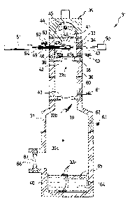
Embodiment 3 (refer to Figures 3-6~
For compound semiconductor crystal:; which have component elements
with a high dissociation pressure, in order to prevent the dissociation of
elements
from melts or from solidified crystals, crystal ~;rowth is often conducted
inside an
ampule or a capsule, and the Bridgeman method is used.
However, with the prior art, it is irr~possible to directly crystallize a
monocrystal from a melt without using a seed crystal. In the monocrystal
manufacturing technology of the present embodiment, a melt of a compound
semiconductor crystal is synthesized, and a monocrystal is directly
crystallized
from this melt without using a seed crystal.
First, the monocrystal manufacturing device is explained. Referring to
Figure 3, the entirety of a monocrystal manufacturing device 71 is shown.
Referring to Figure 4, the top portion of monocrystal manufacturing device 71
is
shown. Referring to Figure 5, the remaining portion of monocrystal
manufacturing
device 71 is shown. Referring to Figures 3-5, monocrystal manufacturing device
71 comprises: a quartz ampule 72 (this corresponds to the capsule), which
vacuum
seals the raw material; a double ellipsoidal gold image furnace 73; a short
furnace
tube 74, which connects to the underside of gold image furnace 73; a drop tube
75, which connects to the bottom of furnace tube 74 and extends vertically to
a
specified length (for example, approximately 14m); a recovery vat 76, which
connects with the bottom of drop tube 75; a hanging copper wire 78
(corresponds
to the means for holding the capsule), which holds ampule 72 inside chamber 77
of gold image furnace 73; a thermocouple 79 for detecting temperature; a
CA 02275640 1999-06-15
PATENT 23 M 1990-4
W'.\USERS\LYMAMwpdata\M I 990-4
deceleration mechanism 80, which is installed somewhere in the middle of the
vertical direction of drop tube 75; a control unit (not shown); and the like.
An air
lock 81 creates a partition between furnace tube 74 and drop tube 75, and an
air
lock 82 creates a partition between drop tube 75 and recovery vat 76.
In double ellipsoidal gold image furnace 73, a pair of ellipsoidal gold
image furnaces 73a, 73a are opposite each other in the horizontal direction.
They
have a single common focal point. Referring to the figure, ampule 72 is held
by
hanging copper wire 78 so that the raw material housed in ampule 72 is
positioned
at the common focal point. The raw material can be heated and melted. A
hermetically sealed terminal 83 is installed at the top of gold image furnace
73.
Hanging copper wire 78 extends from hermetically sealed terminal 83. A Pt-PtRh
thermocouple 79, which also extends from hermetically sealed terminal 83, is
connected so that it can detect the temperature in auxiliary compartment 72b
of
ampule 72. On hermetically sealed terminal 8~t, there are an external terminal
84,
which is connected to hanging copper wire 78, and an external terminal 85,
which
connects to thermocouple 79.
On furnace tube 74 which is in communication with gold image furnace
73, a port 86 and a closing valve 87, which can open and close port 86, are
installed. Port 86 is connected to a vacuum pump and is constructed so that
the air
inside chamber 77 can be evacuated. Air can also be introduced into the
interior
as needed. A transparent air-tight window (not shown) for observing the raw
materials or the melt inside ampule 72 is formed on a terminal attachment
member
98 which attaches hermetically sealed terminal 83. Referring to Figures 3 and
4,
a port 88 and a closing valve 89 which can open and close port 88 are
installed on
the side wall of drop tube 75. Port 88 is connected to a vacuum pump and is
CA 02275640 1999-06-15
PATENT 24 M 1990-4
W .\USERS\LYMAN\wpdata\M 1990-4
constructed so that air can be evacuated from drop tube 75. Port 88 can also
introduce air into the interior as required. Decelerating mechanism 80 is for
decelerating ampule 72 which is falling inside drop tube 75. It is constructed
somewhere along the height direction of the interior of drop tube 75.
Decelerating
mechanism 80 has a pair of right and left rotating plates 80a which are
impelled
in the opposite direction as the arrows by a weak spring. The upper end of
each
rotating plate 80a is joined to the side walls b:y a hinge. When falling
ampule 72
comes into contact with the pair of rotating plates 80a, it is decelerated
and,
without stopping, continues to fall.
Silicone oil 91, which acts to soften the impact of ampule 72 and to cool
ampule 72, and a cushion 92 of a silicone rubber or the like, which is for
impact
absorption, are housed in liquid container 90 at the bottom of recovery vat
76. On
the side wall of recovery vat 76, there is an .opening window 93 for removing
ampule 72. Opening window 93 is constructed so that it can be opened or closed
by an air lock 94.
On the side wall of recovery vat 76, a port 96 and a closing valve 97 which
can open and close port 96 are installed. Port 96 is connected to a vacuum
pump
and is constructed so that air can be evacuated from the inside of recovery
vat 76.
Air can also be introduced into the interior as required.
Referring to Figure 4, quartz ampule 72 comprises: a main compartment
72a, which forms a monocrystal from melt 9.5b of a raw material; an auxiliary
compartment 72b, which is positioned above main compartment 72a and where
an element with a high vapor pressure is evaporated and is dissolved into melt
95b
inside main compartment 72a; a dispersion barrier 72d, which is installed
between
main compartment 72a and auxiliary compartment 72b and in which a small hole
CA 02275640 1999-06-15
PATENT 25 M 1990-4
W:\USERS\I.YMAN\wpdataUyt 1990-4
72c for regulating vapor diffusion is formed. When manufacturing a monocrystal
of a compound semiconductor which contains an element with a high dissociation
pressure, the raw materials are sealed in ampule 72 and dropped.
In this case, raw material, in which each of the component elements have
been measured in advance to achieve the s,toichiometric composition of the
compound semiconductor at its melting point, can be housed inside main
compartment 72a. Or alternatively, raw material, which is a polycrystal which
has
the composition of the compound semiconductor, can be housed in main
compartment 72a. This raw material is heated and melted by gold image furnace
73, and a melt of the compound semiconductor is created.
The raw material of an element with a :high dissociation pressure is stored
in auxiliary compartment 72b. Heating temperature is provided so that, at the
melting point of the element, enough vapor pressure equivalent to dissociation
pressure is generated in order for the melt in main compartment 72a to achieve
the
stoichiometric composition. Ampule 72 and deceleration mechanism 80
correspond to the crystal nucleus generating means.
Next, using monocrystal manufacture device 71, an example of the
manufacture of a monocrystal of In0.97Ga0.03As semiconductor is explained. Ga
and In, which are component elements of In0.97Ga0.03As semiconductor, was
placed at the bottom of main compartment 72;~ of ampule 72. The amount which
is placed inside corresponds to the amount of l;allium (Ga) and indium (In) in
the
melt composition at the melting point of Ino,9,Gao o3As. Similarly, an amount
of As
which is necessary to generate the arsenic (As) pressure to balance the
dissociation
pressure of arsenic at the melting point of In o 9,Gao o3As is placed in
auxiliary
compartment 72b. After storing the raw materials of these component elements,
CA 02275640 1999-06-15
PATENT 26 M 1990-4
W:IUSERS~L.YMAMwpdataUv11990-4
the air inside ampule 72 is evacuated to create a vacuum, and ampule 72 is
then
sealed.
Ampule 72 is hung by passing hanging; copper wire 78 through a ring 72e
at the top of ampule 72. Ampule 72 is positioned at the common focal point of
gold image furnace 73. After the air inside chamber 77 is evacuated to create
a
vacuum, current is run to halogen lamp 73b. The bottom of main compartment
72a of ampule 72 is heated to 1070 degrees C, which is slightly higher than
the
melting point of IrIO.9,Gao o3As, and auxiliary compartment 72b is heated to
approximately 600 degrees C. By the heating. initially, a melt comprising In
and
Ga is formed at the bottom of main compartn-ient 72a. In auxiliary compartment
72b, a portion of As is sublimated, and iit diffuses as a gas inside main
compartment 72a and reacts with the melt of In and Ga. A melt with a
composition of Irlo 9,Gao.o3As is synthesized. In order to allow free fall of
ampule
72 in drop tube 75 and in recovery vat 76, which have had their air evacuated
to
a vacuum in advance, air locks 81, 82 are opened before melt 95b is completely
synthesized,. Next, once the synthesis of melt 95b of IrIO.9~Gao.o3As has been
completed, current is run through hanging copper wire 78, and wire 78 is
melted.
Ampule 72 free falls, and at the same time, the power to halogen lamp 73b is
turned off.
Ampule 72 free falls through a vacuum, and during the fall, it contacts a
pair of rotating plates 80a and is decelerated. Afterwards, its free fall is
continued,
and ampule 72 plunges into silicone oil 91 of recovery vat 76. Finally, it
collides
with cushion 92 of silicon rubber and is stopped.
After initiation of the drop, the inside of ampule 72 changes into a
microgravitational environment. Melt 95b Of IrIO9~Gao,o3As IS levitated and
CA 02275640 1999-06-15
PATENT 27 M 1990-4
W:\USERSU.YMAN\wpda~aUvl 1990-4
becomes spherical due to the action of surface tension. Spherical melt 95b
releases
heat during the fall and becomes supercooled. Ampule 72 is then contacted with
the pair of rotating plates 80a, and the falling speed is reduced. Gravity
operates
inside ampule 72. Melt 95b, which had been levitated, comes into contact with
the
solid surface of the bottom surface of main compartment 72a for a short period
of
time. As a result, a crystal nucleus is generated in a portion of the surface
of
spherical melt 95b. Afterwards, because ampule 72 continues its free fall and
releases heat, crystal growth rapidly proceeds from the crystal nucleus of
melt
95b, which is levitating inside main compartment 72a. The entire spherical
melt
95b becomes a monocrystal 95c of Ino.9,Ga~, o3As. Next, it plunges into
silicone oil
91 and is cooled.
Referring to Figure 6, additional explanation of the behavior starting from
melt synthesis to solidification will be given.
Referring to Figure 6(a), there is shown the conditions of ampule 72
immediately prior to initiation of dropping from gold image furnace 73. Ampule
72 is heated by gold image furnace 73, and the raw material of each of the
component elements melts together to form a synthesized melt 95b of
lr1o.97Gao.o3As.
Referring to Figure 6(b), ampule 72 l:ree falls inside drop tube 75, and
microgravitational conditions are generated in its interior. Melt 95b is
levitated
and becomes spherical due to the action of surface tension. It is hypothesized
that
many of the atoms of the component elements in spherical melt 95b have a
regular
alignment similar to that found in monocrystals.
Referring to Figure 6(c), there is shown the conditions when ampule 72
comes into contact with the pair of rotating plates 80a of decelerating
mechanism
CA 02275640 1999-06-15
PATENT 28 M1990-4
W:\USERS\LYMAN\wpdTta\M 1990-4
80 and decelerates. Spherical melt 95b collides with the bottom surface (solid
surface) of main compartment 72a, and a portion of the surface of spherical
melt
95b contacts with the bottom surface. Because the free energy at this surface
is
lowered, a crystal nucleus is generated at this portion.
Referring to Figure 6(d), ampule 72 passes by decelerating mechanism 80
and is in a free fall state once again. The levitated spherical melt 95b
solidifies,
and a spherical monocrystal 95c is shown.
Referring to Figure 6(e), the state of ampule 72 plunging into silicone
cooling liquid 91 is shown. This monocrystal manufacturing method can be used
to manufacture monocrystals of compound semiconductor crystals which contain
elements with a high dissociation pressure other than the one described.
However,
it should also be clear that this method can be: used for manufacturing
spherical
monocrystals using raw materials of metal materials or insulating materials.
By this monocrystal manufacturing technology, the following advantages
are achieved: spherical monocrystals can be directly manufactured from melts
without using seed crystals; compound semiconductors can be synthesized from
various types of elements; because monoc~ystallization occurs while being
levitated in a spherical shape under microgravitational conditions, a high
quality
monocrystal with extremely few crystal defects can be manufactured; unevenness
in the composition or doping impurities due to the differences in densities of
substances within the melt is reduced; monocrystals of compound semiconductors
of 3 or more elements can be manufactured; spherical monocrystals of various
materials (single element semiconductors, compound semiconductors, metal
materials, insulating materials, and the like) c,an be manufactured; and the
like.
Having described preferred embodiments of the invention with reference
CA 02275640 1999-06-15
PATENT 29 M 1990-4
W:\USERS\LYMAMwpdata\M I J90-4
to the accompanying drawings, it is to be understood that the invention is not
limited to those precise embodiments, and that various changes and
modifications
may be effected therein by one skilled in the an without departing from the
scope
or spirit of the invention as defined in the appended claims.
For example, modes with partial changes, such as the following, can be
implemented for Embodiments 1-3.
1 ) Instead of a halogen lamp, heating means such as a resistance heating
device, high frequency electromagnetic induction heating device, electron beam
heating device, laser heating device, and the Like can be used.
2) When manufacturing a monocrys~tal by dropping an ampule as in
Embodiment 3, it is preferable to separately neat the main compartment, where
melt of a high temperature is made, and a lower temperatured auxiliary
compartment, where volatile elements are evaporated. As a result, it is
preferable
for the main compartment and auxiliary corr~partment to each have their own
temperature-controlled heating source. This is. possible with the existing
art.
3) It is known that spherical melts or spherical melts which are levitated
under microgravitational conditions have a much faster crystal growth rate
compared with when they are under gravity. According to hypotheses by the
inventors relating to this, the configuration of a supercooled melt differs
from that
of a melt under gravity. Because the super<;ooled melt has a regular atomic
alignment similar to monocrystals, once a crystal nucleus is generated at a
point
or at a limited section, the crystal rapidly grows from the crystal nucleus to
form
a monocrystal because the chemical potential of the liquid phase is large.
Therefore, instead of contacting one end of the spherical melt to a solid
substance
in order to generate a crystal nucleus as in the embodiments, one end or a
limited
CA 02275640 1999-06-15
PATENT 30 M 1990-4
W:\USERS\LYMAN\wpdataVv11990-4
section of the spherical melt can be irradiated. with an ion beam during the
fall,
thereby reducing the surface free energy and generating a crystal nucleus. The
monocrystal can be grown from this crystal nucleus.