Note: Descriptions are shown in the official language in which they were submitted.
CA 02275644 1999-06-15
WO 98127655 PCT/SE97/02037
1
PIPELINE ANALOG-TO-DIGITAL CONVERSION
TECHNICAL FIELD OF TSE INVENTION
The present invention generally relates to analog-to-digital
conversion, and more specifically to pipeline analog-to-digital
conversion.
BACKGRODND OF THE INVENTION
An analog-to-digital (A/D) converter is a circuit on the
borderline between the analog domain and the digital domain which
acts as an internnediary in the exchange of information between
the two domains. As the name indicates, an A/D-converter converts
or transforms analog input signals t.o digital output signals. An
A/D-converter could be used for converting analog information
such as audio signals or measurements of physical variables into
numbers consisting of two-level digits or bits; a form suitable
for digital processing. A/D-conver!ters are found in numerous
applications of all modern technologies. They are widely used in
different fields of electronics and communication.
Many systems that use A/D-converter's, such as powerful digital
processing systems, demand high performance A/D-converters. Such
high performance A/D-converters should be able to operate at high
speed and with high accuracy.
A particular type of A/D-converter that operates at high speed i.s
the pipeline A/D-converter. A pipeline A/D-converter is a
discrete-time A/D-converter which comprises a number of fast and
usually relatively simple bit generating and signal processing
stages that are connected in cascade. In a 1-bit per stage
architecture, each stage generates a single output bit.
However, conventional pipeline A/D--converters generally suffer
from limited accuracy. It is knowr.~ that offset errors due to
imperfections in the circuit realizations severely influence the_
accuracy of conventional pipeline A/D-converters. In particular,
pipeline A/D-converters of switched-capacitor type suffer from
CA 02275644 1999-06-15
WO 98/27655 PCT/SE97/02037
2
offset errors due to e.g. DC-offsets, low-frequency noise and
clock induced charge injections. In pipeline A/D-converters which
generate output signals of regular binary code, the offset errors
propagate from stage to stage and accumulate in a strictly
increasing manner during an A/D-conversion, thus limiting the
accuracy of the converter and increasing the distortion.
Relatively large differential and integral non-linearities will
be introduced, and in the worst case scenario output codes might
be missing.
SUb~IA.RY OF TSE INVENTION
It is a general object of the present invention to provide a
pipeline A/D-converter which substantially reduces the
accumulation of errors during a conversion, compared to
conventional pipeline A/D-converters.
It is another object of the invention to provide a pipeline A/D-
converter which has high accuracy and low sensitivity to circuit
realization imperfections.
A further object of the invention is to provide a method for
pipeline A/D-conversion which mitigates the effect of offset
errors on the A/D-conversion.
Yet another object of the invention is to provide a pipeline A/D-
converter having high accuracy while maintaining a low device
count.
These objects are solved by the invention as defined in the
accompanying claims.
In accordance with a general inventive concept, pipeline A/D-
conversion is performed according to an inventive algorithm which
generates a Gray coded digital output signal. A pipeline A/D-
converter comprises a number of cascaded stages through which the -
analog input signal is pipelined. The pipeline A/D-converter
generates the output bits of the digital output signal in a
CA 02275644 1999-06-15
WO 98/Z7655 PCT/SE97/02037
3
discrete-time sequence. According to the inventive Gray coding
algorithm, the output bit generated in a stage determines whether
or not the pipeline signal of that stage is inverted. In a
pipeline A/D-converter based on the Gray coding algorithm
according to the invention, the accumulation of offset errors
will generally be very low.
Furthermore, the fact that the signal inversion is digitally
controlled enables high precision i~~lementations which further
improve the performance of the invent:ive pipeline A/D-converter.
In addition, by modifying the Gray coding algorithm according to
the invention, a low device count implementation is made
possible.
The pipeline A/D-conversion according to the invention offers the
following advantages:
- high accuracy and low distort=ion;
- low accumulation of offset errors;
- low sensitivity to circuit imperfections;
- small differential and integr<~1 non-linearities;
- few missing codes; and
- good dynamic performance, especially for small input
signals.
Other advantages offered by the present invention will be
appreciated upon reading of the below description of the
embodiments of the invention.
3 0 BRIEF DESCRIPTIOTT OF THE DR.A~PINGS
The novel features believed characte=ristic of the invention are
set forth in the appended claims. The invention itself, however,
as well as other features and advantages thereof will be best
understood by reference to the detailed description of the
specific embodiments which follows, when read in conjunction with
the accompanying drawings, wherein:
CA 02275644 1999-06-15
WO 98/27655 PCT/SE97/02037
4
Fig. 1 is a schematic diagram illustrating the general
structure of a pipeline A/D-converter;
Fig. 2 is a schematic diagram illustrating a single stage of
a conventional binary code pipeline A/D-converter
(prior art);
Fig. 3 is a schematic diagram illustrating a single stage of
a pipeline A/D-converter according to the invention;
Fig. 4 is a schematic diagram illustrating an exemplary 4-bit
Gray code pipeline A/D-converter according to the
invention;
Fig. 5 is a schematic flow diagram of a method for pipeline
conversion of an analog input signal into a digital
output signal in accordance with a preferred
embodiment of the invention;
Fig. 6 is a schematic diagram illustrating the transformation
of Gray coded bits into bits of regular binary code;
Fig. 7 is a circuit diagram of a fully differential
realization of a single stage of a Gray code pipeline
A/D-converter in accordance with a currently most
preferred embodiment of the invention;
Fig. 8 is a timing diagram illustrating non-overlapping clock
signals that are utilized in the operation of the
fully differential realization of Fig. 7;
Fig. 9A-B are circuit diagrams of the fully differential
realization of Fig. 7 at consecutive clock phases;
Fig. 10 illustrates a transfer curve of a 5-bit pipeline A/D-
converter based on binary coding;
CA 02275644 1999-06-15
WO 98127655 PCT/SE97/02037
Fig. 11 illustrates a transfer curve of a 5-bit pipeline A/D-
converter based on a Gray coding algorithm according
to the invention; and
5 Fig. 12 is a circuit diagram of a fully differential
realization of a single stage of a D/A-converter
according to the invention..
DETAILED DESCRIPTION OF E~ODIb~NTS OF THE INVENTION
With the intention of briefly explaining the general principle of
a pipeline A/D-converter, reference will now be made to Fig. 1.
Fig. 1 is a schematic diagram illust=rating the general structure
of a pipeline A/D-converter. The pipeline A/D-converter 1
comprises a number, n, of similar bit generating/signal
processing stages 2-1 to 2-n, which are connected in cascade (in
series). For illustrative purposes,all stages are not explicitly
shown. In addition, for reasons of simplicity, a 1-bit per stage
architecture is illustrated. Each o:ne of the stages, except for
the last stage, has an analog input terminal, an analog output
terminal and a digital output terminal. The analog output
terminal of a stage is connected to the analog input terminal of
the following stage. The last stage, i.e. stage 2-n, has an
analog input terminal and a digital output terminal. The stages
2-1 to 2-n are typically controlled by non-overlapping clock
signals ~, and ~2 in combination with some sort of sample-and-
hold circuitry provided in the stages. This gives the pipeline
A/D-converter 1 a discrete-time operation. If, by way of example,
the i-th stage samples on clock pha;~e ~l, the (i-1) -th stage and
the (i+1)-th stage sample on clock phase ~2. The pipeline A/D-
conversion starts when the first stage 2-1 receives and samples
the analog input signal Vi" that is to be converted into a digital
output signal. The first stage 2-1 generates the most significant
bit (MSB) of the digital output in response to the analog input
signal and.further generates a first analog residue signal. The
next stage generates the next output bit, the 2-nd MSB, in
response to the first residue signal from the first stage 2-1,
and further generates a second rea idue signal. The procedure
CA 02275644 1999-06-15
WO 98/27655 PCT/SE97/02037
6
continues until stage n is reached and the n-th output bit, the
LSB, is generated. By definition, when all output bits of the
digital output signal have been generated, the pipeline A/D-
conversion is completed. In general, each stage 2-i samples a
residue signal Vo(i-1) from the preceding stage. The residue
signal Va(i-1) from the preceding stage is also defined as a
local input signal V~,(i) to the current stage. The i-th MSB is
generated in response to this local input signal Vi"(i).
Furthermore, the local input signal V;"(i) is processed in the
stage to generate a new residue signal Vo(i), which is the output
signal of the stage 2-i. Naturally, this output residue signal
Vo(i) will act as a local input signal V;"(i+1) to the next stage.
In order to fully utilize the high-speed capacity of a pipeline
A/D-converter, the converter normally performs a number of A/D-
conversions "simultaneously". In general, the first stage 2-1
generates the MSB, bl-codel, of a first digital code value in
response to a first sample of the analog input signal and further
generates a residue signal which is passed~to the second stage 2-
2. The second stage 2-2 generates the 2-nd MSB, b~-codel, of the
first code value in response to the residue signal from the first
stage 2-1, and generates a residue signal which is passed to the
third stage 2-3. The third stage 2-3 generates the 3-rd MSB, b3-
codel, of the first code value in response thereto. At the same
time the MSB, bl-code2, of a second digital code value is
generated in the first stage 2-1 by processing a second sample of
the analog input signal. The first stage 2-1 and the third stage
2-3 both sample on the same clock phase. In this way, the
pipeline A/D-converter may simultaneously process a number of
~ samples, in different stages of the converter. This increases the
throughput of the pipeline A/D-converter and ensures high-speed
performance.
For a better understanding of the invention it is useful to begin
by explaining the principle and operation of a conventional
pipeline A/D-converter which is based on regular binary coding.
CA 02275644 1999-06-15
WO 98/27655 PCT/SE97/02037
7
Conventionalpipeline A/D-conversion using regular binary code.
In order to avoid misconceptions, the following definition of
regular binary code will be used throughout the disclosure. In
regular binary code, numbers are expressed as linear combinations
of powers of 2:
n
Number = ~ bi . 2n-i ,
i=~
where i and n are integers, and b; :represents a two-level digit
(the i-th bit) . The integer n indicates the number of bits, and
index i indicates the bit position. A coded number is normally
represented as a sequence of bits, where the leftmost bit of the
sequence is the most significant bit (MSB), and the rightmost bit
is the least significant bit (LSB). Hereinafter, regular binary
code will simply be referred to as binary code.
Fig. 2 is a schematic diagram illustrating a single stage of a
conventional pipeline A/D-converter which is based on binary
code. The binary code pipeline stage shown in Fig. 2 comprises
the following functional blocks: a comparator 12, a sample/hold
circuit 13, an amplifier 14, an adder/subtractor 15, and a switch
16.
The stage of Fig. 2 operates as fol:Lows. The input signal V~,(i)
to the i-th stage is passed to the c:omparator 12 which generates
the i-th output bit bi (i-th MSB) of the digital output signal
depending on the sign of the input signal Vin(i). The input signal
V~,(i) is also sampled by the sample/hold circuit 13. The sampled
and held signal is amplified by a factor of 2 in the amplifier
14. The generated binary output bit, in this case bi, determines
whether a reference voltage Vr, hereinafter referred to as the
reference signal, is added to or subtracted from the output
signal of the amplifier 14. The genE_rated binary bit bi controls
a switch 16 such that either the reference signal or its inverse
will be switched into connection with the adder/subtractor 15 and
added to the output signal of the amplifier 14. The output signal
CA 02275644 1999-06-15
WO 98/27655 PGT/SE97/02037
8
of the adder/subtractor 15 is the residue output signal Vo(i) of
the stage. In the next clock phase, this residue output signal
Vo(i) will act as a local input signal Vi"(i+1) to the following
stage.
To realize an n-bit binary code pipeline A/D-converter, n stages,
connected in cascade, are required if a 1-bit per stage design is
considered. In general, non-overlapping clock signals such as ~
and ~z shown in Fig. 1 are utilized to control the operation of
the binary code pipeline A/D-converter. These clock signals are
generated by a clock signal generator (not shown).
The operation of the conventional binary code pipeline A/D
converter can be summarized by an algorithm which is defined by
the following equations:
Vin(1 - 1) - Vin%
(1.1)
Vo(1) = 2 ' Vin(1) -i- (-1)b' ' Vr (1 <- 1 _< n - 1) i vii,(i. ~- 1) = Vo(3.)
and
l, 1f Vin(1) >- 0
b - <_i<-n
(1 ) (1.2)
1f Vin(1) <
where b; denotes the i-th binary output bit, and i is an integer
value . Note that bl is the MSB and bn is the LSB of the digital
output value. It should be understood that the analog input
signal Vi" to be converted into digital forEn is defined as
V~,(i=1), and that the residue output signal Vo(i) of the i-th
stage acts as input signal V;" ( i+1 ) to the ( i+1 ) -th stage . In the
n-th stage, no residue output signal have to be generated, and
therefore i ranges from 1 to n-1 in equation (1.1). This also
means that .the last stage, i . a . the n-th stage, only requires a
comparator which generates the n-th output bit (LSB). -
CA 02275644 1999-06-15
WO 98/27655 PCT/SE97/02037
9
In order to more easily understand the operation of the
conventional binary code pipeline A~'D-converter, an illustrative
example of an ideal binary code conversion of an analog input
signal into a 4-bit digital output ~;ignal will be described with
reference to equations (1.1) and (1.:?). In order to generate a O-
bit signal, 4 stages are required in the pipeline A/D-converter.
In this particular example, assume that the reference voltage is
equal to 1. 0 V and that the input signal V~, (i=1) corresponds to
an input voltage of +0.49 V. The rea idue output signal of each
stage will be generated according to equation (1.1), and the
output bit will be generated according to equation (Z.2). The
A/D-conversion starts when the first stage receives and samples
the analog input signal V~,(i=1).
Generating the first binary bit bl (MfSB) in the first stage, i=1:
V1"(1) - 0.49 ~ bl = 1,
Vo(1) - 2 ~ 0.49 + (-1)1 ~ 1.0 = ().98 - 1.0 = -0.02
Generating the second binary bit bz (2-nd MSB) in the second
stage, i=2:
Vin (2) - Vo(1) ~ bz = 0,
. Vo(2) - 2 ~ (-0.02) + (1)° ~ 1.0 =- -0.04 + 1.0 = 0.96
Generating the third binary bit b, (_4-rd MSB) in the third stage,
i=3:
Vi"(3) - Vo(2) ~ b3 = 1,
Va(3) - 2 ~ 0.96 + (-1)1 ~ 1.0 = :L.92 - 1.0 = 0.92
Generating the fourth binary bit b4 (4-th MSB) in the fourth
stage, i=4:
vin ( 4 ) - Vo ( 3 ) ~ b4 = 1 .
According to the example, the resulting digital output signal
will have 4 bits, and hence the 4-th MSB is the LSB. Bp-
definition, when the LSB has been generated the A/D-conversion is
completed. Accordingly, with a reference voltage of 1.0 V
CA 02275644 1999-06-15
WO 98/27655 PCT/SE97/02037
corresponding to the binary coded value of 1111, an input voltage
of +0.49 V was converted into the binary coded output signal
1011.
5 However, conventional pipeline A/D-converters using binary coding
suffer from high sensitivity to offset errors caused by circuit
realization imperfections. In practical switched-capacitor
realizations, offset errors generally originate from clock
induced charge injections in the clock controlled switches of the
10 A/D-converter, and DC-offsets. Of course other types of errors
such as low-frequency noise may be produced in the conversion.
Anyway, in each stage, or more particularly in the i-th stage, an
offset error OVe(i) will be generated. In a pipeline A/D-
converter, the pipeline signal goes from stage to stage, and the
error in a particular stage is not necessarily identical to that
of the other stages. It is however assumed that part of the error
is correlated and that part is uncorrelated, such that OVe(i) -
OV6 + OVr(i), where ~Vg is a systematic error that is identical to
all stages, and OVr(i) is a random error that is individual for
each stage. The random error OVr(i) has an expectance value equal
to zero. The systematic error OV6 may of course vary from A/D-
converter to A/D-converter. The errors generated in a conversion
will propagate from stage to stage and accumulate in the pipeline
A/D-converter. Referring to equation (1.1) above with
consideration to the error OVe ( i ) - OVg + OVr ( i ) produced in each
stage, the following equation results:
Vo(i) = 2 ~ Vin(i.) + (-1)b' ~ Vz. + OVe + ~Vr(1) (1.3)
Because of the structure of the conventional binary code pipeline
A/D-converter, the systematic part of the errors will accumulate
from stage to stage in a strictly increasing manner. This can be
seen by iterating equation (1.3) from i=1 up until i=n-1, with
the following result:
CA 02275644 1999-06-15
WO 98/27655 PCT/SE97/02037
11
n-1 n-1
Q(n - 1) = 2n 1 . Vin + ~ 2n 1 ~ , (-1)bj . Vr + ~ 2n
j
n-1
'+ ~, 2n 1 7 . OVr(])
j=1
(1.4)
In the n-th stage, no residue output is generated, and for
reasons of simplicity comparator offsets are considered
negligible. Consequently, no offset error is produced in
generating the n-th output bit, Accordingly, the total
accumulated error for an n-bit pipeline A/D-converter using
binary coding, is given by:
n_1 n_1
E bin- ~ 2n 1 ~ ~V6 -F~ ~ 2n 1 ~ ~Vr (j ) ( 1 . 5 )
j=1 j=1
where CVs is the systematic offset error identical for all
stages, and OVr(j) represents the random error produced in the j-
th stage. The systematic offset errors are truly accumulated,
limiting the resolution and increasing the distortion of the
conventional binary code pipeline A/D-converter.
Pipeline A/D-conversion accordin"g~ to the invention.
The general idea according to the present invention is to perform
pipeline A/D-conversion of an analog input signal into a digital
output signal according to an inventive Gray coding algorithm.
Naturally, the generated digital output signal will be in the
form of Gray code. In a first embodiment of the invention, a
first Gray coding algorithm is utilized. According to a preferred
. embodiment of the invention, the first Gray coding algorithm is
modified to fozm a second Gray coding algorithm. In a pipeline
A/D-converter architecture based on either of the first and
second algorithms, the accumulation of errors during a pipeline
A/D-conversion will be very low. In particular, when compared to
a conventional binary code pipeline A/D-converter, the error
accumulation will be substantially reduced.
CA 02275644 1999-06-15
WO 98/27655 PCT/SE97/02037
12
In general, Gray code is known as a sequence of bit patterns in
which adjacent patterns differ in only a single bit. The Gray
code structure is most easily understood by studying table I
given below. Table I illustrates 4-bit Gray code to the left, 4-
bit binary code in the middle and corresponding decimal numbers
to the right.
Table I.
Gra Bina Decimal
0000 0000 0
0001 0001 1
0011 0010 2
0010 0011 3
0110 0100 4
0111 0101 5
0101 0110 6
0100 0111 7
1100 1000 8
1101 1001 9
1111 1010 10
1110 1011 11
1010 1100 12
1011 1101 13
10_0_1 1110 14
1000 1111 15
In both types of code, Gray code and binary code, the rightmost
bit is the least significant bit. It should however be realized
that in Gray code) no specific bit weights can be assigned to the
bits of the coded values . Gray code is sometimes described as a
reflection code, because all the positions of a Gray code value
except f or the leftmost bit position appear as a reflection
around a reflection line, whereas the leftmost position changes
logical state.
Because of the single bit change between adjacent bit patterns,
Gray coding is often used for representing quantized signal
levels and in phase shift keying.
Gray coding has also been used in connection with A/D-converters
in the prior art:
CA 02275644 1999-06-15
WO 98/27655 PCT/SE97/02037
13
According to the article "A High-Speed 7 Bit A/D Converter" in
IEEE Journal of Solid-State Circuits, Vol. SC-14, No. 6, Dec.
1979, by R.J. van de Plassche and. R.E.J, van der Grift, Gray
coding is used in folding-type A/'D-converters. A folding-type
A/D-converter comprises a plurality of parallel stages, and
converts all bits in parallel, as opposed to a pipeline A/D-
converter which uses a sequence of interconnected stages to
sequentially generate.the output signal bit by bit. Since a
folding-type converter determines all bits in parallel, there is
no error accumulation as in pipeline converters. Instead, in the
folding-type A/D-converter, Gray coding is used for reducing the
number of comparators in the circuit realization.
U.S. Patent No. 3,187,325 issued to F.D. Waldhauer on June 1,
1965, discloses a stage-by-stage encoder comprising a
multiplicity of similar stages connected in cascade. The stage-
by-stage encoder of Waldhauer generates Gray code words by using
an all-analog continuous folding technique.
U.S. Patent No. 3,035,258 issued to N.E. Chasek on May 15, 1962,
discloses a pulse code modulation encoder generating Gray code
words by means of an all-analog folding technique. The PCM-
encoder has a plurality of cascaded encoder circuits. Each
encoder circuit comprises a full wave rectifier, a sensing
circuit for determining the instantaneous polarity of the signal
and a sampling network for sampling the signal polarity at a
suitable rate.
Now, the basic principle of the present invention will be
explained with reference to Fi.g. 3 which schematically
illustrates an example of a single stage of a pipeline A/D
converter according to the invention. The pipeline stage of Fig.
3 comprises the following functional blocks: a comparator 22, a
sample/hold circuit 23, an amplifier 24, a inverter 25, a switch
26 and an adder 27.
CA 02275644 1999-06-15
WO 98/27655 PCT/SE97/02037
14
The stage of Fig . 3 operates as follows . The input signal Vin ( i)
to the i-th stage is passed from the preceding stage to the
comparator 22 which generates the i-th bit b; (i-th MSB) of the
digital output signal depending on the sign of the input signal
Vi"(i). The generated output bit is in the form of Gray code. The
input signal is also sampled by the sample/hold circuit 23. The
sampled and held signal is amplified by a factor of 2 in the
amplifier 24. The generated Gray code bit b; determines whether
the output signal of the amplifier 24 or its inverse is added to
a reference voltage Vr, hereinafter referred to as the reference
signal. The reference signal is generated by a conventional
signal source (not shown). The signal inversion is carried out by
the inverter 25. The switch 26, which is controlled by the
generated Gray code bit, determines if the output signal of the
amplifier 24 or its inverse is connected to the adder 27. The
output signal of the adder 27 is the residue output signal Vo(i)
of the stage. In the next clock phase, this residue output signal
Vo(i) will act as a local input signal V;~(i+1) to the following
stage.
To realize an n-bit pipeline A/D-converter according to the
invention, n stages are required if a 1-bit per stage design is
considered. The first n-1 stages are identical to each other,
while the last stage only has a comparator for generating the n-
th output bit. The stages are connected in cascade in accordance
with the overall structure of a conventional pipeline A/D-
converter as shown in Fig. 1. In general, non-overlapping clock
signals are utilized to control the operation of the pipeline
A/D-converter according to the invention. These clock signals are
generated by a clock signal generator (not shown). Naturally, the
A/D-conversion starts when the first stage receives and samples
the analog input signal that is to be converted into digital
form. The analog signal is processed and pipelined through the
consecutive stages of the converter, successively generating the
output bits one by one, until the n-th stage is reached and the_
last output bit is generated.
CA 02275644 1999-06-15
WO 98/27655 PCT/SE97/02037
The operation of the pipeline A/D-converter according to the
invention can be summarized by a first Gray coding algorithm
which is defined by the following equations:
Vin(1 1) Vin
5 (2.1)
Vo(i) = 2 - (- 1)b' ~ Vin(i) + Vr (1 <_ i <_ n - 1) ; Vin(i + 1) = Vo(i)
and
1, if Vin(1) >_ 0
bl 0, if Vin(1) < 0. (1 <_ 1 <_ n) (2.2)
where i is an integer value and b; denotes the i-th output bit
(in the form of Gray code). It should be understood that the
analog input signal V;" to be converted into digital forth is
deffined as Vi"(i=1), and that the residue output signal Vo(i) of
the i-th stage acts as input signal V1"(i+1) to the (i+1)-th
stage. In the n-th stage, no residue output signal have to be
generated, and therefore i ranges from 1 to n-1 in equation
(2.1) . The integer value n represents the number of bits of the
digital output signal.
By studying the first algorithm according to the invention, as
defined above in equations (2.1) and (2.2), it can be seen that
the digital information obtained from the bit decision in a stage
is utilized in generating the residue output signal of that
stage . The bit decision of the following stage is based on this
residue output signal. Accordingly, a decision feed-forward
function is inherent in the algorithm. In practical
implementations of the first Gray coding algorithm according to
the invention, this feed-forward of earlier bit decisions
normally requires some sort of sample-and-hold functionality. It
is the hold operation of the sample-and-hold circuitry that
enables the feed-forward of the ger.~erated digital information.
This will be explained in more detail later, in connection with a
fully differential realization of the invention.
CA 02275644 1999-06-15
WO 98/27655 PCT/SE97/02037
16
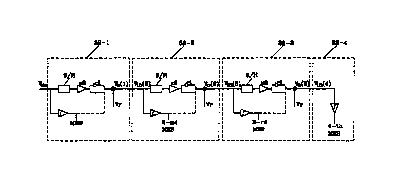
Fig. 4 is a schematic diagram of an illustrative 4-bit Gray code
pipeline A/D-converter according to the invention. The 4-bit
pipeline A/D-converter comprises four stages 32-1, 32-2, 32-3 and
32-4. The three first stages 32-1, 32-2 and 32-3 are identical to
that of Fig. 3, while the last stage 32-4 only includes a
comparator. The analog input signal V;" is received and sampled by
the first stage 32-1 which generates the first Gray code bit bl,
the MSB, of the first digital code value in response to a first
sample of the input signal V;". The first sample of the input
signal Vi" is processed in the first stage 32-1 to generate a
first residue output signal Va(1). This first residue output
signal Vo(1) is passed to the second stage 32-2 as Vi"(2) . In the
second stage 32-2, the second Gray code bit b2, the 2-nd MSB, of
the first code value is generated. The second stage 32-2 further
generates a second residue output signal Vo ( 2 ) , which in turn is
passed to the third stage 32-3 as V~,(3). The third stage 32-3
generates the third Gray code bit b3, the 3-rd MSB, of the first
code value and generates a third residue output signal Ve(3). The
third residue output signal Vo (3 ) is forwarded as Vi" (4 ) to the
comparator of the last stage 32-4, thus generating the fourth
Gray code bit b4, the 4-th MSB, of the first code value.
If the high-speed capacity of the pipeline A/D-converter is to be
utilized, a new sample of the input signal is taken care of by
the first stage 32-1 at the same time as the third MSB of the
first digital code value is generated in the third stage 32-3.
The first stage 32-1 generates the MSB of a second digital code
value in response to this new sample.
For a better understanding of the operation of the Gray code
pipeline A/D-converter according to the invention, an
illustrative example of an ideal conversion of an analog input
signal into a 4-bit digital output signal will now be described
with reference to Fig. 4 and equations (2.1) and (2.2) . In order
to be able to compare the conventional binary code conversion and_
the inventive Gray code conversion, consider the same reference
voltage, 1.0 V, and the same input voltage, 0.49 V, as in the
CA 02275644 1999-06-15
WO 98/27655 PCT/SE97/02037
17
example with the binary code pipeline A/D-converter above. The
residue output signal of each stage will be generated according
to equation (2.1), and the i-th Gray code bit bi is generated
according to equation (2.2).
Generating the first Gray code bit 1~1 (MSB) in the first stage,
i=1:
V;n ( 1 ) - V~, = 0 . 4 9 ~ bl = 1, and
Vo(1) - 2 ~ (-1)1 ~ 0.49 + 1.0 = -0.98 + 1.0 = 0.02.
Generating the second Gray code bit bz (2-nd MSB) in the second
stage, i=2:
Vi"(2) - Vo(1) ~ bZ = 1, and
Vo(2) - 2 ~ (-1)1 ~ 0.02 + 1.0 = -0.04 + 1.0 = 0.96.
Generating the third Gray code bit b3 (3-rd MSB) in the third
stage, i=3:
V;n ( 3 ) - Vo ( 2 ) ~ b3 = 1, and
Vo(3) - 2 ~ (-1)1 ~ 0.96 + 1.0 = -1.92 + 1.0 = -0.92.
Generating the fourth Gray code bit b, (4-th MSB) in the fourth
stage, i=4:
V;"(4) _ Vo(3) ~ b, = 0.
Since the resulting digital output ~ralue should have 4 bits in
this particular example, the 4-th M:>B is the LSB, and when the
LSB has been generated the A/D-conversion is completed.
Accordingly, with a reference voltage of 1.0 V corresponding to
the Gray coded signal or value of 1000, an input voltage of +0.49
V was converted into the Gray coded output signal or value 1110.
By using Table I above, it can be seen that the Gray coded value
1110 corresponds to the binary coded value 1011, which is the
same binary coded value as that generated in the conventional
binary code pipeline A/D-conversion of a +0.49 V input voltage
above. Consequently, the 'resulting digital output signal of the
Gray code converter and the resulting digital output value of the
CA 02275644 1999-06-15
WO 98/27655 PCT/SE97/02037
18
conventional binary code converter are consistent with each
other, although they are generated in different types of code.
However, the propagation of offset errors in the Gray code
pipeline A/D-conversion according to the invention differs
completely from that in conventional binary code pipeline A/D-
conversion. In each stage of a Gray code pipeline A/D-converter
according to the invention, an offset error ~Ve(i) will normally
be generated. In a switched capacitor realization, the main
contribution to the offset in each stage is normally due to clock
induced charge injections in the clock controlled switches and
other DC-offsets. It is assumed that ~Ve(i) - ~V8 + ~Vr(i) , where
CVs is a systematic error that is identical to all stages, and
~Vr(i) is a random error that is individual for each stage. The
random error OVr(i) has an expectance value equal to zero. The
systematic error OVB may of course vary from A/D-converter to
A/D-converter. Because of the structure of a pipeline A/D-
converter based on the first Gray coding algorithm according to
the invention, the systematic part of the offset errors will not
necessarily accumulate in an increasing manner. Referring to
equation (2.1) above with consideration to the error ~VQ(i)
+ OVr(i) produced in the i-th stage, the following equation
results:
Vo(1) = 2 - (-1)bi ' vin(1) + Vr + OV6 + OVx.(1) (2.3)
By iterating equation (2.3) from i=1 up until i=n-1, the result
will be:
n_1 n_1
bj n-2 ~ bk
Vo(n 1) - 2n 1 - ( 1)j ' - Vin + ~ 2n 1 ~ ' (-1)k j+, + 1
j=1
n-1 n-1
n-2 ~ bk n_2 ~ b~c
+ ~ 2n-1-j . (-1)k=j+i .+- 1 - ws + ~ 2n-1-~ . (-1)k=i+i . OVz,(j) +
j-1 J-1
+ OVr(n - 1)
(2.4)
CA 02275644 1999-06-15
WO 98/27655 PCT/SE97/02037
19
In the n-th stage, no residue output is generated, and for
reasons of simplicity comparato:r offsets are considered
negligible. Consequently, no error i.s produced in generating the
n-th output bit. Therefore, the totaa accumulated error for an n-
bit pipeline A/D-converter based on the first Gray coding
algorithm according to the invention, is given by:
n_7 n_1
n 2 ~ bk n- 2 ~ b
~Gray - ~ 2n 1 ~ . (-1)k=i+i + 1 ~ DV6 -~ ~ 2n 1-7 . (-1)k=i+ik . eVr(j)
J-1 J-_1
+ OVr(n - 1)
(2.5)
where OVB is the systematic offset error identical for all
stages, and ~Vr(j) represents the random error produced in the j-
th stage.
Now, compare the total accumulated error for the binary code
pipeline A/D-converter and the inventive Gray code pipeline A/D-
converter by studying expression (1.5) and expression (2.5). The
mean value and variance of the random error component for Gray
code conversion according to the invE:ntion are identical to those
for binary code conversion. In particular, the mean value of the
random error component is equal to zero. Accordingly, for
simplicity and clarity, the random errors will be disregarded in
the remaining part of the disclosure.
Since
n-i
bk
(-1) k i + i _ ~1, ( 3 . 1 )
the following relation holds true:
n-i
_ ~ bk _
2" 1-~ . (-1)k=j+' < 2n-1-~_ (3.2)
CA 02275644 1999-06-15
WO 98/27655 PCT/SE97/02037
Regarding the systematic offset errors, the following relation
results:
n-1
n-2 ~ bk n-2
IEGra I - ~ 2n 1 ~ . (-1)k=i+i + 1 . eVs < ~ ~ n 1 . -
,, 2 j + 1 evs -
j=1 j=1
n-1
5 ~ 2n 1 ~ eVs - IE binl ( 3 . 3 )
Strictly mathematically speaking, equation (3.3) shows that the
total accumulated systematic error in an n-bit Gray code pipeline
A/D-conversion according to the invention is smaller than or
10 equal to the total accumulated systematic error in an n-bit
binary code pipeline A/D-conversion. In practice, however, the
Gray code accumulated systematic error will almost always be
smaller than the binary code accumulated systematic error. It is
useful to give a brief and intuitive explanation of this fact. As
15 is well known, the systematic error evB produced in each stage
will propagate through the remaining stages of the A/D-converter.
However, in the pipeline A/D-converter based on the first Gray
coding algorithm according to the invention, in each stage, the
pipeline signal is selectively subjected to an inversion,
20 depending on the Gray code bit generated in the stage. Since the
generated Gray code bits vary between the discrete states 0 and'1
more or less randomly, depending on the particular application,
the systematic errors associated with the pipeline stages will
sometimes be added to and sometimes subtracted from the total
systematic error accumulated up until that point. Consequently,
the systematic offset errors generated during an A/D-conversion
will not necessarily accumulate in an increasing manner, and the
total accumulated systematic error will lie substantially closer
to zero in a Gray code conversion according to the invention than
in a conventional binary code conversion.
Accordingly, with regard to the sensitivity to circuit
imperfections, the Gray code pipeline A/D-converter according to
CA 02275644 1999-06-15
WO 98/27655 PCT/SE97/02037
21
the invention has a significant advantage over its binary code
counterpart.
For illustrative purposes, the error accumulation for an
exemplary 4-bit binary coded value, 0110, generated
conventionally, and the error accumulation for the corresponding
4-bit Gray coded value 0101, gener<~ted in accordance with the
invention, will be compared in the following. Since a 4-bit value
is considered in this particular example, n is equal to 4. The
systematic offset error in generating each bit is assumed to be
+0.02 V. For simplicity, as explained above, the random errors
are assumed to be zero.
Binary code accumulated error:
According to equation (1.5) for a binary code pipeline A/D-
converter, the total accumulated offset error in generating the
binary coded value 0110 will be:
Ebin (n=4) = 2Z-0 . 02 + 210 . 02 + 2°~0 . 02 = 0 . 08 + 0. 04 + 0 . 02
= 0 .14 .
Gray code accumulated error:
According to equation (2.5) for a Gray code pipeline A/D
converter according to the invention, the total accumulated
offset error in generating the Gray coded value 0101 (bl=0, bz=1,
b,=0, bq=1) will be:
s~~Y(n=4) - 2~~ (-1) '1'°'0.02 + 21~ (-1) '°'0.02 + 0.02 =
- 4~ (-1) 0.02 + 2~ (1) 0.02 + 0.02 = -0.1)8 + 0.04 + 0.02 = -0.02.
3 0 It can be seen that ~ s~,Y ' < ~ F:~;~ ~ . The Gray code error
accumulation according to the invention is generally considerably
lower than the binary code error accumulation. This is a property
directly related to the term (-1)b~ associated with V~,(i) in the
first Gray coding algorithm defined above in equations (2.1) and_
(2.2). In a statistical sense, the total accumulated systematic
CA 02275644 1999-06-15
WO 98!27655 PCT/SE97/02037
22
error in a pipeline A/D-conversion according to the invention is
reduced in the majority of cases.
Fig. 5 is a schematic flow diagram of a method for pipeline
conversion of an analog input signal into a digital output signal
according to a preferred embodiment of the invention. It is
assumed that the resulting digital output signal has a
predetermined number, n, of output bits b;, where i is an integer
ranging from 1 to n. The pipeline A/D-conversion based on the
first Gray coding algorithm according to the invention basically
works as follows . In step 41, the analog input signal V;s, (i=1) =V~,
is inputted for A/D-conversion. At this point i is equal to 1,
indicating that the first output bit is to be generated in the
first stage. Next, in step 42, the analog input signal Vi"(i=1) is
compared with a zero level to generate the first Gray code output
bit blin accordance with equation (2.2). If i is equal to n, i.e.
if all the bits of the digital output signal have been generated
(YES) at this point (step 43) the A/D-conversion is completed and
the procedure ends. However, the digital output signal generally
comprises more than a single bit (NO), and the procedure
continues with step 44. In step 44, the input signal is sampled
and held. Next, in step 45, the sampled and held signal is
subjected to an amplification by two and selectively, depending
on the Gray coded output bit bl previously generated in step 42,
to a signal inversion. The amplified and selectively inverted
signal is added to a predetermined reference signal in step 46,
to generate a first residue output signal Vo(i=1). This residue
output signal Vo(i=1) will act as a next input signal V;"(i=i+1=2)
in the generation of the next output bit b2 in the following
3a stage. Thus, the integer i is incremented by one. The procedure
continues in step 42, in which the next input signal Vi"(2) is
compared to a zero level to generate the second Gray code output
bit bz. The procedure continues in accordance with the flow
diagram shown in Fig. 5 until all n output bits have been
generated.
CA 02275644 1999-06-15
WO 98/27655 PCT/SE97/02037
23
If the high-speed feature of the pipeline A/D-conversion is
utilized, several samples of the input signal are simultaneously
processed in different stages. A first sample of the input signal
is pipelined and processed through the consecutive stages. As
soon as the residue output signal of the first stage has been
sampled by the next stage, the first stage is ready to receive a
next sample of the input signal. Accordingly, in the next
sampling clock phase of the first stage, the MSB of the next
digital code value is generated by the first stage and the
pipeline process is initiated for this new sample. This increases
the throughput of the pipeline A/D-conversion.
It should be understood that the specific order of the
amplification by two, and the selective signal inversion in step
45 generally is not critical for t:he pipeline A/D-conversion
according to the invention. It is possible to selectively, in
dependence on the generated output bit bi, invert the sampled and
held signal before amplifying it by two. This also holds true for
the Gray code pipeline stage shown in Fig. 3.
Naturally, the digital output signal of the Gray code pipeline
A/D-converter according to the invention is in the form of Gray
code. However, if the pipeline A/D-converter according to the
invention is to be used in a system having equipment designed to
work with normal or regular binary code, it may be more feasible
to convert the Gray coded output signal into an output signal of
regular binary code. Consequently, in this case, the inventive
pipeline A/D-converter generating Go_ay coded signals, further
incorporates, as a final stage, means. for digitally transforming
the Gray coded output signal into an output signal of regular
binary code. Fig. 6 is a schematic diagram illustrating an
illustrative transformation of 4 bits of Gray code into 4 bits of
regular binary code by using simple digital gates XOR-1, XOR-2,
XOR-3. The Gray code bits, here denoted G(i), are transformed
into bits, here denoted B(i), of binary code according to the_
following known relations:
CA 02275644 1999-06-15
WO 98/27655 PCT/SE97/02037
24
B (1) = G (1) ;
B (i) = G (i) ~ B (i - 1) , 2 <_ i _< n ( 4 .1 )
where n is the number of bits of the code values. In the example
of Fig. 6, n is equal to 4. The Gray code MSB, G(1), transforms
into the binary code MSB, B ( 1 ) without any change . The remaining
Gray code bits are transformed into binary code bits by using the
corresponding digital XOR-gates. This digital transformation does
not introduce any offset errors. Accordingly, by using the
inventive Gray code pipeline A/D-conversion in combination with
the above digital Gray code-to-binary code transformation, it is
possible to perform a pipeline A/D-conversion, of which the final
output signal is in the form of regular binary code, and still
maintain low accumulation of offset errors.
In order to facilitate the circuit realization of each stage in a
Gray code pipeline converter according to the invention, equation
(2.1) is rewritten in the following way:
Vo(1) = 2 - (-1)b' ' Vin(1) + Vr - {2 - Vin(1) + (-1)y'' ' Vr } ~ (-1)b' (5.1)
By modifying the first Gray coding algorithm of equations (2.1)
and (2.2) using the mathematical derivation of expression (5.1)
the following second Gray coding algorithm results:
Vin(1 - 1) - Vin
Vo(i) _ ~2 ' Vin(i) + (-1)bi ' Vr} ' (-1)b' (1 <- i _< n - 1) ; Vin(i + 1) =
Vo(i)
{5.2)
and
1, if Vin(1) > 0
bi - {1 <- i <- n) (5.3)
0, if Vin(i) < 0
This second Gray coding algorithm minimizes the number of
operational amplifiers (OPAMPS) required in a circuit realization
CA 02275644 1999-06-15
WO 98/27655 PCT/SE97/02037
of a pipeline A/D-converter according to the invention. In a
single stage, the number of required OPAMPS goes from 2 for a
realization based on the first algorithm, to 1 for a realization
based on the second algorithm. In a pipeline A/D-converter
5 comprising a plurality of stages, the improvement is
considerable. Consequently, by realizing a pipeline A/D-converter
according to the second Gray coding algorithm given above, a low
device count is obtained. Besides, the accumulation of systematic
offset errors is very similar to that: of a pipeline A/D-converter
10 which is based on the first algorithm, as will be shown below.
Fig. 7 is a circuit diagram of a i_°ully differential switched-
capacitor realization of a single stage of a pipeline A/D-
converter in accordance with a preferred embodiment of the
15 invention. The circuit realization is based on the second Gray
coding algorithm given by equations (5.2) and (5.3). Assume that
the i-th stage of a pipeline A/D-converter is considered. When
dealing with differential A/D-c:onverter realizations, a
differential input signal to the stage is considered. The
20 differential input signal has a positive part Vn(i) and a
negative part Vn(i). They have the same magnitude but opposite
polarity. In the same way, a predetermined differential reference
signal, Vr and -Vr, is utilized by t:he A/D-converter stage. The
pipeline A/D-converter stage 50 basically comprises capacitors
25 C1, C2, an operational amplifier (OPAMP) 51, a switch arrangement
52, a comparator 53, a clock signal generator 54 and control
switches S1 to S5.
Each one of the capacitors Cl, C2 is connected to a respective
switch S1. The switches S1 selectively connects the differential
input of the stage 50 to the capacitors C1, C2. The capacitance
of the capacitors C1 is equal to that of the capacitors C2. In
addition, the capacitors C1 are selectively connected, via the
switches S4, S5, to the differential reference signal. The
switches S1 and the capacitors C2 are referred to as input signal
switch-capacitor units. The switches S1, S4, SS and the capacitors
CA 02275644 1999-06-15
WO 98/27655 PCT/SE97/02037
26
C1 are referred to as input/reference signal switch-capacitor
units. The OPAMP 51 has two input terminals and two output
terminals, and operates with an internal Gammon mode feedback
function. Each of the input terminals of the OPAMP 51 is
connected to a pair of capacitors C1 and C2. Each one of the
capacitors C2 is selectively connected, via switch S2, in
parallel over a respective pair of input-output terminals of the
OPAMP 51. Furthermore, there is a switch S, connected in parallel
over each pair of input-output terminals of the OPAMP 51. The
switch arrangement 52 has two input terminals and two output
terminals, and comprises four switches S4, S5. The comparator 53
has two input terminals and an output.terminal. Preferably, the
comparator 53 is a latched comparator. The clock signal generator
54 generates a first set of clock signals ~l and ~2, of a
predetermined and non-overlapping timing, and a second set of
clock signals ~S4 and ASS of a predetermined timing and with
values that depend on the generated output bits. If the input to
the stage is sampled at ~1, the clock signals ~5, and mss are
generated according to the following relations:
(5.4)
where bi represents the opposite logical state of bi. If the
input to the stage is sampled at ~z, the clock signals ~S4 and ASS
will be generated based on ~1 instead of ~z.
It should be understood that normally the clock signal generator
54 is common for the complete pipeline A/D-converter, each stage
passing its generated output bit to the clock signal generator
54.
The differential input signal to the stage is passed to the
switches S,; and the capacitors C1, C2 associated thereto. In_
addition, the differential input signal to the stage is passed to
the input terminals of the comparator 53. The output terminal of
CA 02275644 1999-06-15
WO 98127655 PCT/SE97/02037
27
the comparator 53 is connected to the clock signal generator 54.
The capacitors C1 are selectively connected, via switches S~, SS
associated thereto, to the reference signal source (Vr,-Vr). The
output terminals of the OPAMP 51 are connected to the input
terminals of the switch arrangement. 52. The output terminals of
the switch arrangement 52 normally constitutes the output
terminals of the complete pipeline stage 50. Accordingly) the
differential output signal of the switch arrangement 52 is the
output of the stage.
Note that the output terminals of th.e switch arrangement 52 for a
particular stage will be connected in series with the switches S1
of the following stage. This series connection of switches may
increase the signal path resistance. A way of avoiding this
series connection of switches would be to remove the switches S1
and instead duplicate the switch arrangement 52. In this case,
there will be two parallel switch arrangements 52, one of which
is directly connected to the capa~~itors C1 of the subsequent
stage while the other one is directly connected to the capacitors
C2 of the subsequent stage.
The selected topology illustrated in Fig. 7 has been chosen for
simplicity of explanation.
Fig. 8 is an example of a timing diagram illustrating the timing
of the clock signals ~1 and ~2 utili.zed in the fully differential
realization of Fig. 7. The operation of the converter stage 50 is
controlled by these clock signals, and the clock signals ~~ and
defined above. More specifically, ~l controls switches S, and
S3; ~2 controls switches SZ; ~S4 controls switches S4; and ~s
controls switches S5. Furthermore,, ~1 triggers the latched
comparator 53. In this realization eacample, a switch is turned on
when the corresponding clock signal goes high, and turned off
when the clock signal goes low.
CA 02275644 1999-06-15
WO 98/27655 PCT/SE97/OZ037
28
In short, the pipeline stage 50 operates as follows. In the first
clock phase, when ~1 is high, the differential input signal to
the stage 50 is sampled by the capacitors C1, C2, and the
comparator 53 generates the i-th MSB, bi. The OPAMP 51 is reset;
auto-zeroed. In the next clock phase, when ~~ is high, the input
signal to the stage 50 is amplified by a factor of 2, and the
reference signal is added or subtracted depending on the i-th MSB
generated by the comparator 53 in the previous clock phase. This
is basically effected by the particular coupling of the OPAMP 51,
the capacitors C1, C2 and the switches S1, S2 and the switches S4,
SS associated to the capacitors C1. Furthermore, the output
signal of the OPAMP 51 is selectively inverted by the switch
arrangement 52 in dependence on the generated output bit, thus
generating the output of the stage 50.
The capacitors C1, C2 and the control switches S1 associated
thereto act as a sample-and-hold circuit of switched-capacitor
type. Because of the hold operation of this sample-and-hold
circuit, and the non-overlapping timing of the clock signals that
control the comparator 53 and the switch arrangement 52,
respectively, the bit decision of the comparator 53 and the
selective inversion of the switch arrangement 52 are separated in
time. This separation in time enables the feed-forward of the
generated digital output to the switch arrangement 52.
It should be understood that the signal inversion executed in the
switch arrangement 52 utilizes the digital information from the
bit decision in the comparator 53, and decides whether or not the
input to the switch arrangement 52 should be inverted based on
this digital information. The signal inversion is preferably
implemented as a digitally controlled polarity shift. In the
fully differential realization 50 of Fig. 7 the inversion is
performed by interchanging the polarity of the differential
signal by using the digitally controlled switch arrangement 52.
In this way, the signal inversion is realized with very high-
accuracy. The high precision of the signal inversion further
CA 02275644 1999-06-15
WO 98/27655 PCT/SE97/02037
29
improves the accuracy of the pipeline A/D-converter according to
the invention.
Furthermore, it is important to understand that in this
particular embodiment of the invention, the output bit generated
by the comparator 53 is also utilized to decide whether or not
the polarity of the differential reference signal should be
shifted. This polarity shift is effE~cted by the switches S4, SS
connected to the reference signal source (Vr,-Vr).
For a better understanding of the fully differential realization
shown in Fig. 7, the operation of the pipeline A/D-converter
stage 50 according to the invention will now be explained in more
detail at the consecutive clock phase's ~1 and ~2. Figs. 9A-B are
circuit diagrams of the fully differential realization of the
pipeline A/D-converter at consecutive clock phases. The circuit
diagrams have been reduced to illustrate only those parts of the
pipeline stage 50 that are pertinent at the considered clock
phase. Open switches and unconnected elements will generally not
be illustrated.
Fig. 9A illustrates the pipeline stage 50 at the clock phase when
~1 is high. The switches S1 and S3 are turned on. The differential
input signal ( V n(i) , Vi (i) ) of the i-t:h stage 50 is sampled by the
input capacitors C1 and C2:
V n(i) = Vo (i - 1) ; V n(1) = V n
(5.5)
V n(i) = Vo(i - 1) ; V n(1) = Vin
where Vo (i - 1) , Vo (i - 1) denotes the differential residue
output signal of stage i-1, anal V n , Vin denotes the
differential input signal to the f~~rst stage of the pipeline
A/D-converter.
CA 02275644 1999-06-15
WO 98/27655 PCT/SE97/02037
The differential input signal of the i-th stage is also passed to
the input terminals of the comparator 53, which generates the i-
th MSB, bi, according to the following relation:
1, if V n(i) - V n(i) >_ 0
5 bi - (5.6)
0, if V n(i) - Vi (i) < 0
The input to the comparator 53 is differential and the output is
digital. Furthermore, in the clock phase of ~1, the OPAMP 51 is
reset to enable suppression of the DC-offset of the OPAMP.
Fig. 9B illustrates the pipeline stage 50 during the clock phase
when ~Z is high. The switches Sz are turned on. Accordingly, the
capacitors C2 are connected in parallel over the OPAM~ 51. The
reference signal source Vr,-Vr is switched into connection with
the capacitors C1. The sign of the reference signal that is
switched into connection with the respective capacitor C1 on each
side of the differential structure will be either positive or
negative, depending on the generated output bit b;. This is
expressed as (-1)b' ~ Vr in equation (5.2) . The clock signals ~S
and ASS that control the switches S4 and S5, connected to the
capacitors C1, depend on the generated output bit. All the
switches S4 and SS are illustrated as open, although in reality,
either the switches S4 or the switches SS will be closed in this
clock phase. Because of the coupling of the OPAMP 51 and the
capacitors C1, C2, the differential input signal to the stage
sampled onto the capacitors C1, C2 in the previous clock phase
will come out amplified by a factor of 2 at the output terminals
of the OPAMP 51. In addition, the reference signal will
contribute to the output of the OPAMP 51; either as a negative
term or as a positive term, depending on the output bit generated
by the comparator 53 as explained above. Finally, the output
signal of the OPAMP 51 is passed to the switch arrangement 52.
The switch arrangement 52 performs a signal inversion, also in
dependence on the output bit generated by the comparator 53 in
CA 02275644 1999-06-15
WO 98/27655 PCT/SE97/02037
31
the previous clock phase. More specifically, the states of the
switches S4 and SS controlled by the clock signals ~S4 and
respectively, determine whether or not the switch arrangement 52
interchanges the polarity of the differential signal.
Accordingly, the output of the switch arrangement, and indeed,
the output of the complete pipeline ~;tage 50, will be given by:
Vo (i) _ ~2 ~ V n(i} + (-1)bi ' Vr ~ ~ (-1)bi
(5.7}
Vo (1} _ {2 ' V n(1) - (-1)b' ' Vr + OVe(1}~ ' I;-1}b'
which is rewritten as:
; ;
b 1-1 ~ b
i k
Vo . ( 1)j=1. Virn~ 2i_j . (-1)k=i+~+ .
(i) -f- 1 V
-
2i
r
j=1
t
i i
bi i-1 ~ b
Vc . ( 1)i=1. V ~ _
(i) in 7 . (_1)k + .
- _ 2i ~+i 1 Vr
2i
j=1
i
~ bt
+ _ (-1)k ' OVe(j)
~ 21 '
'
'
j=1
(5.8}
OVe(i) represents an error voltage produced in the i-th stage.
For simplicity it is assumed that t:he error OVe(i) produced in
the i-th stage is introduced at the O:PAMP 51 on the negative side
of the differential realization. This error voltage is
representative of a number of different types of errors voltages.
Switches provided at high impedance nodes normally inject a small
charge, a so called clock induced charge, which gives rise to a
DC-offset error voltage. In a differential realization, these
offset errors will ideally exclude each other. However,
asymmetric switch pairs in regard to clock induced charge
injection will generate a DC-offset. In general, there is a DC-_
offset inherent in the OPAMP. However, in accordance with the
invention, this offset is minimized by resetting the OPAMP and
CA 02275644 1999-06-15
WO 98/27655 PCT/SE97/02037
32
storing the offset in the capacitors associated with the OPAMP.
In the following, all errors together, including low-frequency
noise as well, in a stage, are represented by the error voltage
~Ve (i) . The error voltage ~Ve (i) consists of two teens, ~V6 and
OVr(i). The term CVs represents a systematic offset error that is
identical for all stages, whereas the term OVr(i) represents a
random error that is individual for each stage. It has been
assumed that the random errors are zero, and therefore OVe ( i ) is
equal to the systematic error CVs. In the following OVe(i) will be
substituted by CVs.
To realize an n-bit pipeline A/D-converter, n stages are
required. However, the last stage) i.e. the n-th stage, only has
to include a comparator which compares the output signal of the
(n-1)-th stage with a zero level to generate the n-th output bit)
the LSB. Non-overlapping clock signals such as those shown in
Fig. 8 are normally used to control the operation of the pipeline
A/D-converter. If the input to the i-th stage is sampled on clock
phase ~l, the input to the (i+1)-th stage is sampled on clock
phase ~2. The i-th MSB precedes the (i-1)-th MSB by half a clock
period.
The residue output signal of the (n-1)-th stage is given by:
n-~
n-i
~ b~ ~ bk
Vo (n ~ ~- .
~=i P n_1_7 k=i+i 1 Vr
- 1) - 2n i . (-1) 2 . (-1)
. Vin -~-
j=1
n-1 n-1
bj n-2
k
Vo(ri - 1) = 2n 1 ' (-1)j-' ~' 2n 1 ~ - (-1)k=j+i+ .
~ V n - 1 Vr
j=1
n-i
n-1 ~ bk
+ ~, 2n i ~ . (-1)k'
. DV
j=~
(5.9)
CA 02275644 1999-06-15
WO 98127655 PCT/SE97/02037
33
The residue output signal of the (n-1)-th stage acts as input
to the n-th stage:
V n(n) = Vo(n - 1)
(5.10)
V n(n) = Vo (n - 1)
where the n-th output bit b;, the LSB is generated according to:
1, i f V n (n) - Vi (n) >_ 0
bi - (5.11)
0, if V ri(n) - V n(n) < 0
The last term of Vo(n - 1) in expre~~sion (5.9) above represents
the total accumulated error generated in an n-bit pipeline A/D-
converter based on the second Gray coding algorithm according to
the invention:
n-1
n-1 _ _ E bk
EGray - ~ 2n 1 ~ ' (-1) k j - evs ( 5 .12 )
j=1
The expression (5.12) is very similar to the expression (2.5)
given above (under the condition that the random errors are
assumed to be zero); the indexation differs slightly. It can be
shown that the accumulated error given by (5.12) is less than the
accumulated error for a binary code counter part.
It should be understood that single-ended A/D-converter
realizations based on the fully differential realization
described above are easily obtained.
In accordance with a currently most preferred embodiment of the
invention, the switches S1 are removed and instead the switch
arrangement 52 is duplicated in parallel and the output terminals
of the parallel switch arrangements 52 are connected directly to
the capcitors C1 and C2 of the following stage.
CA 02275644 1999-06-15
WO 98/27655 PCT/SE97/02037
34
Simulations
The operation of a conventional binary code pipeline A/D-
converter and the Gray code pipeline A/D-converter proposed
according to the invention have been simulated in an algorithm
simulator. Both static and dynamic performances have been
studied.
Regarding the static behavior, the introduction of systematic
offset errors has been simulated and the effects will be briefly
described with reference to Figs. 10 and 11. In Fig. 10 there is
illustrated a transfer curve of a 5-bit pipeline A/D-converter
based on binary coding. Fig. 11 illustrates a transfer curve of a
5-bit pipeline A/D-converter based on the first Gray coding
algorithm according to the invention. In each case, the magnitude
of introduced systematic offset errors is assumed to be 1.5 LSB.
It is seen from Fig. 10 that the simulated systematic offset
errors gives the transfer curve for the binary code A/D-converter
apparent non-linear characteristics. The transfer curve departs
from the ideal stepped transfer curve, and missing codes, such as
code 16, are introduced in the binary code pipeline A/D-
converter.
In the transfer curve of Fig. 11 for the Gray code pipeline A/D-
converter according to the invention, the only noticeable effect
of the simulated systematic offset errors is the introduction of
a small gain error. The slope or gain of the transfer curve has
changed, but otherwise the ideal stepped form of the curve
remains unchanged.
In addition, the proposed Gray code architecture of pipeline A/D-
converters also turns out to improve the operation performance in
comparison to conventional binary code pipeline A/D-converters in
several other ways. The integral non-linearity and the
differential non-linearity of the inventive Gray code A/D-
converter are much smaller than their binary code counterparts.
The signal-to-noise-and-distortion ratio (SNDR) and the spurious-
CA 02275644 1999-06-15
WO 98/27655 PGT/SE97/02037
free dynamic range (SFDR) are improved significantly by the
proposed Gray code conversion.
In summary, both theoretical derivations and system simulations
5 have shown that the proposed Gray code pipeline A/D-converters
are superior to conventional pipelinES A/D-converters. The new and
inventive pipeline A/D-converter architectures based on the Gray
coding algorithms according to the invention are well suited for
high-accuracy as well as for low-distortion applications.
10 In accordance with a second aspect of the invention, the inverse
of the principles utilized for pipeline A/D-conversion is used
for pipeline digital-to-analog (D/A) conversion. Accordingly, the
second aspect of the invention relates to the conversion of
digital input signals into analog output signals. In accordance
15 with a preferred embodiment of the second aspect of the
invention, a Gray coded digital signal is converted into an
analog output signal according to <~n algorithm defined by the
following equation:
20 Vg(i) _ ~ ~ [Vg(i + 1) - Vrl ~ {-1)b9~i), i - Td, N - 1, . . . ,1 {6.1)
where bg(1) designates the MSB and bg(N) designates the LSB,
assuming an N-bit D/A-converter. The subscript g indicates that
the digital input is Gray code. Vg(i) represents the intermediate
25 analog quantity associated with the i-th LSB, where 2 <_ i <- N,
and V9 (N+1) - 0 . The output quantity of the D/A-converter is Vgo"t
which is equal to Vg(1) . Vr denotes a predetermined reference
quantity. The D/A-conversion starts from the LSB. The
intermediate quantities, the reference quantity and the output
30 quantity can be charges, voltages o:r currents depending on the
particular circuit realization.
By iterating equation (6.1) until i=1, the result will be:
CA 02275644 1999-06-15
WO 98/27655 PCT/SE97/02037
36
N 1 E b9(>>
vgout - Vg (1) _ ~, i (-1)j ' ' Ur ( 6 . 2 )
i=1 2
Suppose there is an offset error OVg(i) in generating each of the
intermediate quantities and the output quantity. Referring to
equation (6.1) above with consideration to the error ~Vg(i), the
following equation results:
Vg(i) = 2 ' [Vg(i + 1) - Vr + ~Vg(i.)J ' (-1)b9(i) (6.3)
By iterating equation (6.3) until i=1, the result will be:
N 1 E b9 t) N 1 E b9(>>
vgout - Ug(1) _ ~, i (-1)5 ' ' yr + ~ i (-1)~ ' ' ~Vg(1)
i=~ 2 i=~ 2
(6.4)
Therefore, the total accumulated error in a complete D/A-
conversion according to the invention is determined by:
1 E b9 (J)
~Vgout - ~ i (-1)3 ' - ~Vg (i) ( 6 . 5 )
i=1 2
The total accumulated error in a D/A-conversion according to the
invention is considerably lower than that in conventional D/A-
conversions. In particular, in comparison to binary code pipeline
D/A-conversion, a corresponding improvement as that between
pipeline A/D-conversion according to the invention and
conventional binary code pipeline A/D-conversion is obtained.
Fig. 12 is a circuit diagram of a fully differential realization
of a pipeline D/A-converter in accordance with the invention. The
circuit implementation of Fig. 12 realizes the algorithm given by
equation (6.1). Just as the fully differential A/D-converter
realization of Fig. 7, the D/A-converter realization of Fig. 12
CA 02275644 1999-06-15
WO 98/27655 PCT/SE97/02037
37
is of switched-capacitor type with digitally controlled switches.
The non-overlapping clock signals ~1 and ~Z that control the
operation of the pipeline D/A-converter are also illustrated in
Fig. 12. The N-bit D/A-converter of Fig. 12 comprises N cascaded
stages, of which only the i-th stage is illustrated in detail.
The inteztnediate output Vg(i) of stage i is the input to stage i-
1. The input Vg(N+1) to stage N is equal to zero. The output Vg(1)
of stage 1 is the final output Vgo"t of the pipeline D/A-
converter. In order to process the data properly, the successive
bits of the Gray coded input signal are delayed by half a clock
N-i
cycle starting from the LSB. The notation z 2 indicates the
N - i
delay by 2 clock cycles, where N > i ? 1. Since a D/A-
conversion is the inverse of an A/D-conversion, referee a is made
to the description in connection with the A/D-convert r of Fig.
7, 8 and 9A-B for a more detailed understanding of the D/A-
converter of Fig. 12. However, it should be understo d that in
each stage of the pipeline D/A-converter accordin to the
invention, a subtraction of the reference and an amplif cation by
a factor of 0.5 are performed. It should also be under tood that
the Gray code bits of the digital ;signal determines hether or
not the inverse function is realized..
The embodiments described above are nnerely given as exa ples, and
it should be understood that the invention is no limited
thereto. It is of course possible to embody the in ntion in
specific fortes other than those described without depa ting from
the spirit of the invention. Further modifications an itt~prove-
ments which retain the basic underlying principles dis losed and
claimed herein are within the scope and spirit of the 'nvention.