Note: Descriptions are shown in the official language in which they were submitted.
CA 02276201 1999-07-19
t
- 1 -
IMAGE DATA CONVERSION PROCESSING DEVICE AND
INFORMATION PROCESSING DEVICE HAVING THE SAME
BACKGROUND OF THE INVENTION
This invention relates to an image data conversion
'processing device for converting into television signals
image data which are developed in plural kinds of
. developing formats in a memory, and an information
processing device having the image data conversion
processing device.
The information processing device comprises a
personal computer including a memory and a processing
unit, for example. The information processing device is
connected to a cathode ray tube ( CRT ) , and image data
output from the memory is displayed on the CRT. At this
time, the image data is developed in various kinds of
developing formats into a video random access memory
(VRAM). ~ ' .
The image data comprises 320 pixel ( dots ) on each
line, and the total number of lines is 200. Resides, the
image data comprises 640 dots x 400 lines or 640 dots x 480
lines . The frame ( screen ) of the CRT is divided into a
display frame area for displaying the image data and a
non-display frame area.
A program has a mode data corresponding to an image
mode of the image data for displaying the image data on
the screen. The mode data represents the size of the non-
28708-1D
CA 02276201 1999-07-19
- 2 -
display frame area, the number of dots of the display
frame area in a horizontal direction, a flyback period and
,a read-out frequency for each dot.
A device for controlling the CRT to display the image
data serves to set a horizontal scanning frequency 3lKHz
on the basis of the mode data of the program when the image
data comprises 640 dots x 480 lines. This device reads out
the image data at a read-out frequency 28MHz from the VRAM
in accordance with the set horizontal scanning frequency.
The CRT displays the image data on the display frame area
thereof on the basis of the mode data.
On the other hand, this device sets a horizontal
scanning frequency lSKHz when the image data comprises 320
dots x 200'lines. In this case', the device reads out the
image data at a read-out frequency 2lMHz from the VRAM in
accordance with the horizontal scanning frequency.
Further, the device sets a horizontal scanning frequency
24KHz when the image data comprises 640 dots x 400 lines.
In this case, the device reads out the image data at a
read-out frequency 25MHz from the VRAM in accordance with
this horizontal scanning frequency. Various CRTs are
individually provided in accordance with image data which
are developed in various kinds of developing formats .
As described above, the device for controlling the CRT
to perform its display operation enables the CRT to
display image data corresponding to the image mode by
setting a horizontal scanning frequency.
28708-1D
CA 02276201 1999-07-19
- 3 -
In addition, a multi-CRT capable of displaying.
various image data of 320 dots x 200 lines, 640 dots x 400
lines and 640 dots x 480 lines for example has been
recently proposed. In this case, an information
processing device having the program outputs a composite
signal to the multi-CRT. The composite signal comprises
horizontal synchronizing signal and a vertical
synchronizing signal of 31/24/15. On the basis of the
composite signal, the multi-CRT displays image data of RGH
signals which are output from the information processing
device.
On the other hand, there is a television device which
is generally used for a domestic purpose in contraposition
with the CRT and the multi-CRT as described above. The
horizontal scanning frequency of this television device
is specified to l5KHz (accurately 15.73426KHz), and an
effective line number is specified to 400 lines. In the
television device, one frame is displayed with two fields
'through an interlaced scanning operation in which the
frame is scanned with interlacing lines.
It has been increasingly required that this type of
4
television device is connected to the information
processing device to promote the propagation of the
information processing device. In this case, a scan
converter for converting image data into a television
signal is required. The scan converter is provided with a
. change-over switch for selecting any one of the plural
28708-1D
CA 02276201 1999-07-19
_ 4
horizonal scanning frequencies as described above, and on
the basis of a set ( selected ) horizontal scanning
frequency the scan converter converts the image data to be
displayed by the information processing device. The
television device displays an image on the frame thereof
on the basis of the television signal.
As described above, when the television device is
connected to the information processing device, the scan
converter converts image data transmitted in an analog
form into digital signals and then stores the digital
signals into an internal VRAM. Further, the scan converter
converts the image data to television signals which will
be interlaced at a horizontal scanning frequency l5KHz,
and output the converted television signals to the
'television device.
When the line number of image data to be developed in
the VRAM exceeds 400 lines of a television frame, the
conventional scan converter displays only an image
portion corresponding to 400 lines, which is specified by
an adjusting volume. Therefore, in this case, there occurs
a problem that the other image data corresponding plural
lines other than the above 400 lines is not displayed on
the television frame ( screen ) . In order to solve this
problem, the image data is compressed by the scan
converter.
If the image data is uniformly compressed by the scan
converter, an image which should not be compressed might
28708-1D
CA 02276201 1999-07-19
- 5 -
be compressed. For example, the information processing
device frequently outputs image data of 640 dots x 480
V
lines and image data of 640 dots x 420 lines at a
horizontal scanning frequency 3lKHz, for example. In this
case, the image data of 640 dots x 420 lines can be
displayed on the television screen, whereas the image data
of 640 dots x 480 lines can not be displayed on the
television screen.
The scan converter serves to compress the image data
of 640 dots x 480 lines to 640 dots x 420 lines at a
constant compression rate, however, it also compresses,
at the constant compression rate, the image data of 640
dots x 420 lines which is originally unnecessary to be
compressed.
Further, use of the scan converter as described above
induces a problem that an user must select a horizontal
scanning frequency through the change-over switch. The
composite signal may be used to remove an user' s
manipulation of the change-over switch. The composite
signal is a synchronizing signal, and comprises signals
having respective frequencies . In this case, code
information representing each of the frequencies is not
transmitted, and thus the frequency can not be immediately
identified on the basis of the composite signal.
Accordingly, for example, a frequency detector for
detecting each frequency is provided to the scan
converter. The manipulating operation of the change-over
28708-1D
CA 02276201 1999-07-19
-6-
switch can be omitted by using a detection result of the
frequency detector. However, in this case the circuit
construction of the scan converter is more complicated.
Further, when the scan converter is used, the image
data to be displayed, which is developed in the
information processing device, is converted from a
digital signal to an analog signal, and then the analog
signal is re-converted to the digital signal again by the
scan converter. Therefor, there occurs a problem that the
image quality of the image data to be displayed on the
television device is deteriorated.
Still further, in the conventional scan converter,
the image data transmitted from the information
processing device is converted to the television signal
merely through the interlaced scanning operation.
Therefore, a flicker occurs on the screen of the
television device, and thus a displayed image is obscure.
SUMMARY OF THE INVENTION
An object of this invention is to provided an image
data conversion processing device capable of
automatically generating television signals having
4
excellent display performance on the basis of various
kinds of image data to be developed on a VRAM with keeping
a single hardware construction, and an information
processing device having the image data conversion
processing device thus constructed.
In order to attain the above ob j ect, the image data
28708-1D
CA 02276201 1999-07-19
x
converting device according to this invention converts
image data of plural lines, which are stored in a storing
unit and can be developed in various kinds of developing
formats, into television signals having a predetermined
5 number of lines. The image data converting device includes
an issue unit, plural line storing unit and a generating
unit. The issue unit serves to issue an image data
transmitting instruction to the storing unit in
accordance with a period which is specified by a ratio of
' 10 the line number of image data to be converted and a
predetermined line number of the television signal.
The plural line storing units serve to cyclically
store line by line the image data transmitted from the
storing unit on the basis of the transmission instruction
of the issue unit.
The generating unit serves to multiply the image data
stored in the line storing units by an interpolative
coefficient corresponding to a developing format of an
image data to be developed in plural interpolative
coefficients which are beforehand set in correspondence
with plural kinds of developing formats, in synchronism
with the horizontal synchronizing signal of the
television signal, thereby generating the television
signal.
According to this invention, the image data of various
kinds of developing formats can be automatically
converted to the television signals.
28708-1D
CA 02276201 1999-07-19
- 8 -
Further, the image data conversion processing device
according to this invention converts image data, which are
stored in a storing unit and can be developed in plural
kinds of developing formats, into a television signal
having a predetermined line number. The image data
comprises plural lines.
The image data conversion processing device of this
invention includes a mode managing unit and a conversion
processing unit. The mode managing unit serves to manage a
mode data corresponding to the line number of the image
data.
The conversion processing unit serves to renew the
conversion of the image data in accordance with the mode
data supplied from the mode managing unit to convert the
image data corresponding to at least plural mode data to
television signals.
Still further, the information processing device
according to this invention executes plural programs
corresponding to different image modes. The image data
includes a predetermined image mode. The program includes
a mode data having information for the image mode of the
image data thereof or a specified information.
The information processing device executes the plural
programs and has a processing unit for processing the mode
data and the image data . The processing unit includes an
image storing unit and a conversion processing unit . The
image storing unit serves to store the program containing
28708-1D
CA 02276201 1999-07-19
-9-
the mode data and the image data. The conversion
processing unit serves to subject the image data stored in
the image storing unit to a predetermined conversion in
accordance with the mode data to thereby convert the image
data to the television signal.
Still further, the image data conversion processing
device according to this invention converts the image
data, which can be developed in the plural kinds of
developing formats, to a television signal of a
predetermined line number. The image data comprises
plural lines . The image data conversion processing device
includes an even storing unit, an odd storing unit, a
signal generating unit and a format conversion processing
unit.
The even storing unit serves to store image data of
even lines in the image data to be converted while the odd
storing unit serves to store image data of odd lines in
the image data to be converted .
The signal generating unit generates a horizontal
synchronizing signal for the television signal, and also
generates plural rate data llrhich are determined by a ratio
of the line number of the image data and the predetermined
line number of the television signal in correspondence
with the plural kinds of developing formats.
The format conversion processing unit serves to
' convert the image data of the even and odd lines supplied
,from the even storing unit and the odd storing unit into
28708-1D
CA 02276201 1999-07-19
- 10 -
the format of the television signal using the horizontal
synchronizing signal and the rate data corresponding to
the developing format of the image data to be converted.
According to the information processing device of
this invention, the even storing unit and the odd storing
unit are provided and a calculation is carried out by
reading out the image data of the even and odd lines, so
that the construction of the format conversion processing
4
unit can be simplified.
Still further, the information processing device of
this invention converts the image data, which are stored
in a storing unit, to a television signal having a
' predetermined line number. The image data comprises plural
,lines.
One frame of the television signal comprises plural
fields. The information processing device of this
invention includes a linear interpolating unit, plural
field storing units, a synchronizing signal generating
unit and a field control unit.
The linear interpolating unit serves to linearly
interpolate image data of two lines of an image data line
supplied from the storing unit and an image data line
adjacent to the above image data line using a
predetermined an interpolative coefficient, thereby
generating the television signal.
The plural field storing units are provided at the
input or output side of the linear interpolating unit to
28708-1D
CA 02276201 2000-03-O1
28708-1D
11
store the respective lines on a field basis. The synchronizing
signal generating unit serves to generate the horizontal
synchronizing signal and the vertical synchronizing signal of
the television signal.
The field control unit serves to perform write-in and
read-out operations of the image data field by field for the
plural field storing units on the basis of the synchronizing
signal which is generated in the synchronizing signal
to generating unit.
According to the information processing device of
this invention, the image data is subjected to the processing
field by field to generate the television signal.
As described above, according to the image data
conversion processing device and the information processing
device of this invention, the television signal having
excellent display performance can be automatically generated
from the image data of various kinds of developing format with
keeping a single hardware construction, and thus the
manipulation of the user can be removed.
In accordance with the present invention, there is
provided an information processing device for converting image
data to a television signal, comprising: processing means for
executing plural programs corresponding to different image
modes, in which image data has a predetermined image mode, each
program has a mode data for storing information corresponding
to the image mode of the image data thereof, and for processing
the mode data and the image data, wherein said processing means
includes image storing means for storing the image data; and
conversion processing means for conducting a predetermined
conversion on the image data stored in said image storing means
CA 02276201 2000-03-O1
28708-1D
lla
in accordance with the mode data provided by said program to
convert the image data to the television signal.
In accordance with the present invention, there is
also provided an information processing device for converting
image data to a television signal comprising: processing means
for executing a program; image storing means for storing image
data made by the program, wherein image data is in different
sizes based on said program; and conversion processing means
for changing a conversion of the image data and for conducting
the changed conversion, wherein said conversion processing
means is capable of converting a plurality of kinds of the
image data to a signal which is an interlaced television signal
having a predetermined number of lines.
In accordance with the present invention, there is
further provided an information processing method for
converting image data to a television signal, comprising: step
of executing plural programs corresponding to different image
modes, in which image data has a predetermined image mode, each
program has a mode data for storing information corresponding
to the image mode of the image data thereof; step of processing
the mode data and the image data; step of storing the image
data; and step of conducting a predetermined conversion on the
image data stored by said step of storing in accordance with
the mode data to convert the image data to the television
signal.
In accordance with the present invention, there is
further provided an information processing method for
converting image data to a television signal comprising: step
of executing a program; step of storing image data made by the
program, wherein image data is developable in different sizes
based on said program; and step of processing conversion of
CA 02276201 2000-03-O1
28708-1D
llb
said image data; wherein said step of processing conversion to
said image data further including; step of changing a
conversion of the image data and step of conducting the changed
conversion, wherein said step of conducting is capable of
converting a plurality of kinds of the image data to a signal
which is an interlaced television signal having a predetermined
number of lines.
BRIEF DESCRIPTION OF THE DRAWINGS
Fig. 1 is a block diagram showing an information
processing device having an image data conversion processing
device of a first embodiment of this invention;
Fig. 2 is a block diagram showing the basis
construction of the image data conversion processing
CA 02276201 1999-07-19
- 12 -
device as shown in Fig. 1;
Fig. 3 is a flowchart showing an operation of the
image data conversion processing device as shown in Fig.
2;
Fig . 4 is a block diagram showing the typical
construction of the image data conversion processing
device as shown in Fig. 1;
Fig. 5 is a block diagram showing a main part of the
construction as shown in Fig. 4;
Fig . 6 is an explanatory diagram for calculation of an
interpolative coefficient;
Fig. 7 is another explanatory diagram for calculation
of an interpolative coefficient;
Figs . SA and 8H show an embodiment of a management
data of a management table;
Fig. 9 is a time chart for an operational processing
of the embodiment;
Fig. 10 is another time chart for the operational
processing of the embodiment:
420 Fig. 11 is an explanatory diagram showing a television
signal generating processing;
Fig. 12 is another explanatory diagram showing the
television signal generating processing;
Fig. 13 is another explanatory diagram showing the
television signal generating processing;
i
Fig . 14 is an explanatory diagram for introducing an
interpolative coefficient;
28708-1D
CA 02276201 1999-07-19
- 13 -
Fig. 15 is a diagram showing the basic construction of
the image data conversion processing device according to a
second embodiment of this invention;
Fig. 16 is a flowchart for the operation of the image
data conversion processing device as shown in Fig. 15;
Fig. 17 is a block diagram showing a semiconductor
memory unit in the typical construction of the image data
conversion processing device according to the second
embodiment of this invention;
Fig. 18 is block diagram showing a peripheral circuit
containing a format conversion processing unit in the
typical construction of the image data conversion
processing device of the second embodiment of this
invention;
Fig. 19 is a block diagram showing the construction of
a conversion processing control unit;
Fig. 20 is block diagram showing the construction of
the calculation processing unit;
Fig. 21 is a timing chart for a display section of a
first television signal of an ODD field;
Fig. 22 is a timing chart for a display section of a
second television signal of an ODD field;
Fig. 23 is a schematic diagram for generation of a
television signal of an ODD field;
Fig. 24 is a diagram for calculation of a
semiconductor memory read-out address and an
interpolative coefficient;
28708-1D
CA 02276201 1999-07-19
4
- 14 -
Fig. 25 is a timing chart for a display section of a
' first television signal of an EVEN field;
Fig. 26 is a timing chart for a display section of a
second television signal of an EVEN field;
Fig. 27 is schematic diagram for generation of a
television signal of an EVEN field;
Fig. 28 is a block diagram showing the construction of
a first modification of the second embodiment;
Fig. 29 is a timing chart for a display section of a
first television signal of an ODD field of the first
modification;
Fig. 30 is a timing chart for a display section of a
second television signal of an ODD field of the first
modification;
' 15 Fig. 31 is a schematic diagram for generation of a
television signal of an ODD field;
Fig. 32 is a timing chart for a display section of a
first television signal of an EVEN field of the first
modification;
Fig. 33 is a timing chart for a display section of a
second television signal of an EVEN field of the first
modification;
Fig. 34 is a schematic diagram for generation of a
television signal of an EVEN field;
Fig. 35 is a block diagram showing the construction of
a second modification of the second embodiment;
Fig. 36 is a block diagram showing the construction of
28708-1D
CA 02276201 1999-07-19
- 15 -
a conversion processing control unit;
Fig. 37 is a block diagram showing the construction of
a calculation processing unit;
Fig. 38 is a block diagram showing the basis
construction of the information processing device
according to a third embodiment of this invention;
Fig. 39 is a flowchart for the operation of the
information processing device as shown in Fig. 38;
Fig. 40 is a block diagram showing the typical
construction of the information processing device of the
third embodiment according to this invention;
y
~~ Fig. 41 is a flowchart for the operation of the
information processing device as shown in Fig. 40;
Fig. 42 is a diagram showing a transversal filter;
Fig. 43 is a diagram showing a linear interpolating
circuit;
Fig . 44 is a diagram showing an example of an
interpolative coefficient value; and
Fig. 45 is a diagram showing the construction of a
linear interpolating circuit 120.
DETAILED DESCRIPTION OF~THE PREFERRED EMBODIMENTS
Preferred embodiments of the image data conversion
processing device and the information processing device
having the image data conversion processing device will be
hereunder described with reference to the accompanying
drawings.
< First Embodiment >
28708-1D
CA 02276201 1999-07-19
- 16 -
Fig. 1 is a block diagram showing the construction of
an information processing device having an image data
conversion processing device of a first embodiment
according to this invention.
In Fig. 1, the information processing device
comprises a personal computer, for example. The
information processing device includes a CPU 31, an image
memory 32, a VRAM 2, a mode managing unit 33, and a read-
out control unit 34. The information processing device 30
4
is connected to an external television device 40.
The image memory 32 serves to store a program and
image data. The program has a mode data storing
information corresponding an image mode of an image data
thereof or specified information.
~ The CPU 31 serves to conduct a processing on the
program and the image data from the image memory 32. This
image data has a predetermined image mode . The CPU 31
executes plural programs in which the image modes are
different from each other, and it receives the mode data
contained in the program and the image data .
The CPU 31 also outputs the image data of the image
memory 32 to the VRAM 2, and outputs the mode data to the
mode managing unit 33. The image data comprises plural
lines, and each line comprises plural dots. In this
construction, the image data whose image modes are
different from each other have different line numbers of
data. The mode data is a data corresponding to the line
28708-1D
CA 02276201 1999-07-19
- 17 -
number.
The VRAM 2 serves to store image data of various kinds
j of developing formats . The image data are stored into the
VRAM 2, for example, in a developing format of 320 pixel
( dots ) x 200 lines, 640 dots x 400 lines or 640 dots x 480
lines. The image data may be stored in another developing
format.
The mode managing unit 33 serves to manage the mode
data corresponding to the line number of the image data
which will be developed in the VRAM 2 and converted. The
read-out control unit 34 constitutes an image data
conversion processing device. The read-out control unit
34 renews a conversion mode ( manner ) of image data in
accordance with the mode data supplied from the mode
managing unit 34 to convert image data corresponding to at
least plural mode data into television signals.
The image data for television signals represents a
predetermined line number. The read-out control unit 34
subjects the image data to a predetermined conversion
which is determined on the basis of a line number ratio of
the above predetermined line number and the mode data,
thereby converting the image data corresponding to at
least plural mode data into television signals.
In this construction, a managing table 220 as
described later is provided to the read-out control unit
34. The managing table 220 includes a first conversion
information for converting to image data having the line
28708-1D
CA 02276201 1999-07-19
- 18 -
number of the television signal image data in which the
image line number to be converted is larger than the line
number of the television signal. The managing table 220
also includes a second conversion information for
converting to image data having the line number of the
television signal image data in which the image line
number to be converted is smaller than the line number of
the television signal.
The read-out control unit 34 selects any one of the
first and second conversion information, and performs the
conversion of the image data on the basis of the selected
conversion information.
The read-out control unit 34 may alter a read-out
range of data to be read out from the VRAM 2 in accordance
with the mode data, and further it may carry out the
conversion in accordance with the scanning frequency of
the television signal.
In this construction, an image output from the read-
but control unit 34 is displayed on a television device
40. The information processing device 30 may be designed
in one-housing structure.
° A. Hasic Construction of Image Data Conversion Processing
Device of First Embodiment
Fig. 2 is a block diagram showing the basic
construction of the image data conversion processing
device. The image data conversion processing device 1
includes s VRAM 2, plural line buffers 3, a generating
28708-1D
CA 02276201 1999-07-19
- 19 -
unit 4, a first counter 5, a second counter 6, a table 7
and an issue unit 8.
The VRAM 2 serves to store image data to be converted
to a television signal. The image data stored in the VRAM
2 is developed with the program. The image data comprises
640 dots x 400 lines or 640 dots x 480 lines, for example.
The plural line buffers 3 are connected to the VRAM 2
as shown in Fig. 2, and each of the line buffers 3 serves
to cyclically store the image data transmitted from the
"10 VRAM 2 line by line.
The generating unit 4 is connected to the plural line
buffers 3, and it serves to generate the horizontal
synchronizing signal and the vertical synchronizing
signal of a television signal. The generating unit 4
multiplies the image data stored in the line buffer 3 in
synchronism with the horizontal synchronizing signal by
an interpolative coefficient which is assigned to the
image data, and generates the television signal by adding
these multiplied results.
That is, the generating unit 4 carries out a linear
interpolation of the image data of two image data lines of
an image data line for a television signal line and an
adjacent image data line thereto using a predetermined
value which is beforehand set as the interpolative
coefficient, thereby calculating a signal level, and also
calculates, an average in signal level between the two
television signal lines of the linearly interpolated
28708-1D
CA 02276201 1999-07-19
- 20 -
television signal line and a television signal line
,adjacent thereto.
Further, the generating unit 4 generates a television
signal through the calculation of the average value in
signal level between the two image data lines of the image
data line corresponding to the television signal line and
the ad j acent image data line thereto using the
predetermined value which is beforehand set as the
interpolative coefficient.
The first counter 5 cyclically counts the horizontal
synchronizing signal of the television signal on the basis
of the mode data supplied from the mode managing unit 33
at a period which is specified' by the mode data.
The table 7 manages interpolative coefficients and
identifying clock numbers for the horizontal
synchronizing signal of the television signal in
accordance with the developing formats of the image data.
These managing data are defined in accordance with the
developing formats of the image data stored in the VRAM 2,
and has periodicity to the horizontal synchronizing
signal of the television signal.
The table 7 sets the interpolative coefficients and
the identifying clock numbers for the mode data supplied
from the mode managing unit 33 as ob j ects to be output .
The table 7 uses a count value of the first counter 5 as an
access address to output an interpolative coefficient
having periodicity corresponding to the count value in the
28708-1D
CA 02276201 1999-07-19
- 21 -
interpolative coefficients and the identifying clock
numbers which are objects to be output. The interpolative
coefficient thus output is supplied to the generating unit
4 while the identifying clock number is output to the
issue unit 8.
The second counter 6 counts the clock number of the
horizonal synchronizing signal of the television signal.
The issue unit 8 issues an instruction for transmitting
the image data to the VRAM 2 through the comparison
between the identifying clock number output from the table
7 and the count value counted by the second counter 6.
Next, the operation of the image data conversion
processing device thus constructed will be described.
Fig. 3 is a flowchart showing the operation of the
image data conversion processing device as shown in Fig .
2.
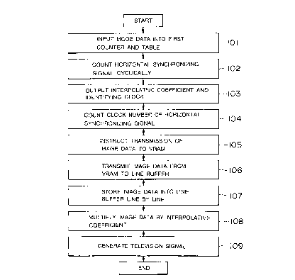
First, a mode data for an image data which will be
developed in the VRAM 2 is supplied to the first counter 5
and the table 7 ( step 101 ) . The first counter 5 performs
its cyclic counting operation of the horizontal
synchronizing signal of the 'television signal at the
period defined by the mode data ( step 102 ) .
In response to the counting operation as described
above, the table 7 outputs an interpolative coefficient
and an identifying clock number having periodicity
defined by the above count value in the interpolative
boefficients and the identifying clock numbers which are
28708-1D
CA 02276201 1999-07-19
- 22 -
objects to be output in accordance with the mode data
( step 103 ) . The second counter 6 counts the clock number
of the horizontal synchronizing signal of the television
signal (step 104).
The issue unit 8 compares the identifying clock number
qutput from the table 7 and the count value of the second
counter 6. When the identifying clock number is coincident
with the count value, a transmission instruction for a
series of image data which is sequential to a previous one
410 is issued ( step 105 ) . That is, the issue unit 8 issues the
transmission instruction of the series of image data
sequential to the previous one in accordance with the
periodicity which is defined by the ratio in line number
between the line number of the image data developed in the
VRAM 2 and the line number of the television signal.
Accordingly, when the line number of the image data of
the VRAM 2 is larger than the line number of the
television signal, the issue unit 8 issues th'e
transmission instruction of the image data in accordance
with a short period. On the other hand, when the line
number of the image data is smaller than the line number
of the television signal, the issue unit 8 issues the
transmission instruction of the image data in accordance
with a long period .
In response to the transmission instruction of the
issue unit -8, the image data is transmitted from the VRAM
2 to the line buffer 3 ( step 106 ) . In this case, the image
28708-1D
CA 02276201 1999-07-19
4
- 23 -
data is first sequentially transmitted with the image data
' of the top line at a transmission starting point every
transmission unit of a predetermined number of lines. When
the transmission of the image data is completed,
subsequently the image data is sequentially transmitted
with the image data of the next line to the top line at a
transmission starting point every transmission unit of a
predetermined number of lines . When the transmission of
the image data is completed, the image data is
sequentially transmitted with the top line thereof at a
transmission starting point again every transmission
unit. As described above, the image data is transmitted
while the transmission unit using the image data of the
top line as the transmission starting point and the other
transmission unit using the image data of the next line to
the top line as the transmission starting point are
alternately selected.
The line buffer 3 cyclically latches the image data
'transmitted from the VRASM 2 line by line ( step 107 ) . In
response to the latch operation as described above, the
generating unit 4 multiplies the image data latched in the
line buffer 3 and the interpolative coefficient output
from the table 7 in synchronism with the horizontal
synchronizing signal of the television signal ( step 108 ) .
The generating unit 4 generates the television signal by
adding these multiplied results (step 109).
That is, the line buffer 3 renews the latched image
28708-1D
CA 02276201 1999-07-19
- 24 -
data at a short period when the line number of the image
data developed in the VRAM 2 is large. When the line
number of the image data is small, the line buffer 3
renews the latched image data at a long period. In
response to the latch operation of the image data by the
line buffer 3, the generating unit 4 can generate the
television signal while reducing (compressing) the image
data developed in the VRAM 2.
There is a case where many line buffers 3 are prepared
such that the number of the line buffers 3 is larger than
the line number of the image data required for the
generating processing of the television signal by the
generating unit 4. In this case, the issue unit 8 issues
the transmission instruction of the image data at such a
timing as to keep the line buffers 3 whose number is
sufficient to store the image data required for the
generation of the television signal in the write-in
processing of the image data into the line buffers 3. In
this case, the write-in speed of the image data into the
line buffers 3 is set to be higher than the read-out speed
of the image data from the line buffers 3.
A set value of the interpolative coefficient used in
this case is set by the generating unit 4. This set value
is calculated as follows. The image data of two image
data lines adjacent to an image data line corresponding to
a television signal line are subjected to the linear
interpolation to calculate a signal level. The
28708-1D
CA 02276201 1999-07-19
- 25 -
interpolative coefficient is so set that a television
signal having an average value between the above signal
level and a similar signal level obtained for a television
signal line adjacent to the above television signal line
~,s generated.
In accordance with the set value of the interpolative
coefficient, the generating unit 4 calculates the signal
level of each television signal by obtaining the signal
level of a linear interpolative value of two image data
sandwiching the corresponding image data line which is in
reduced (compressed) relation with the television signal.
Subsequently, the generating unit 4 determines the final
signal level of the television signal by calculating the
average value of the two adjacent television signals thus
obtained.
As described above, the generating unit 4 determines
the signal level of the television signal while reducing
the image data of the VRAM 2. Further, the generating unit
4 averages the signal level between the ad j acent
television signals. Through this operation, flickerless
television signals are generated from all image data of
the VRAM 2. Further, the generating unit 4 generates
television signals of interlaced scanning in accordance
with the set value of the interpolative coefficient and
the alternately-transmitted image data.
H. Image Data Conversion Processing Device having Typical
construction of First Embodiment
28708-1D
CA 02276201 1999-07-19
4
- 26 -
Next, the image data conversion processing device
having typical construction will be described. Fig. 4 is a
block diagram showing the typical construction of the
image data conversion processing device.
In Fig. 4, the image data conversion processing device
reads out the image data stored in the VRAM 2 in
accordance with the mode data from the mode managing unit
33. Further, it reduces the image data to display all the
image data stored in the VRAM 2 on the television device
40, and determines the signal level of the television
signal. Still further, it generates a flickerless
television signal by averaging the signal level between
adjacent television signals.
In Fig. 4, an RGH matrix circuit 10 converts the image
data of RGH components read out from the VRAM 2 to the
image data of YUV components. A low-pass filter (LPF) 11
removes noise components of the image data of U-components
converted by the RGB matrix circuit 10. A LPF 12 removes
noise components of the image data of V-components
converted by the RGH matrix circuit 10.
A multiplexer 13 selects the image data of any one of
the two low-pass filters 11 and 12. A line buffer 14-i
( i=1 to 4 ) serves to cyclically and successively store the
image data of the Y-component converted by the RGH matrix
circuit 10 and the image data of the component selected by
the multiplexer 13 line by line.
A selector 15 selects the image data stored in the
28708-1D
CA 02276201 1999-07-19
27
line buf fer 14-i . A logical operation circuit 16 generates
a television signal by subjecting the image data stored in
the line buffer 14-i to a reducing operation and a flicker
removing operation. A demultiplexer allocates the
selector 18 with the U and V-component television signals
of the television signals output from the logical
operation circuit 16, which are selected by the
multiplexer 13.
The selector 18 selects any one of the image data
converted by the RGB matrix circuit 10 and the television
signal output from the logical operation circuit 16. An
NTSC encoder 19 encodes the television signal output from
the selector 18 into an NTSC signal. A D/A converter 20
converts a digital signal output from the NTSC encoder 19
to an analog signal and then output the analog signal to
the television device 40.
A line buffer write-in control circuit 21 controls the
write-in operation of the image data into the line buffer
14-i on the basis of the mode data from the mode managing
unit 33. An interpolative coefficient generating circuit
22 generates an interpolative coefficient which is
required for the logical operation circuit 16 to perform
the reducing operation and the flicker removing operation
as described above on the basis of the mode data and clock
signals CLKSO and CLKS1. An interpolative coefficient
,generating circuit 22 outputs the interpolative
coefficient to the logical operation circuit 16.
28708-1D
CA 02276201 1999-07-19
- 28 -
An NTSC synchronizing signal generating circuit 23
generates an NTSC synchronizing signal containing a
horizontal synchronizing signal and a vertical
synchronizing signal on the basis of a clock of 28.63MHz
for example. An NTSC synchronizing signal generating
circuit 23 outputs an NTSC synchronizing signal to an
interpolative coefficient generating curcuit 22.
4
In this construction, each of the line buffer 14-i,
the selector 15 and the logical operation circuit 16 is
respectively provided in pairs ( i. e. , two groups of line
buffers, selectors and logical operation circuits are
provided ) in correspondence with the ODD field and the
EVEN field of the television signals. In Fig. 4, one group
i
of the line buffer 14-i, the selector 15 and the logical
operation~circuit 16 are illustrated. The write-in
operation of the image data into the line buffer 14-i is
executed at 28. 6MHz ( 8fsc ) . The operation of the logical
operation circuit 16 is executed at 14.3MHz ( 4fsc ) in
synchronism with the generation of the television
signals. That is, the write-in operation of the image data
into the line buffer 14-i and the operation of the logical
operation circuit 16 are executed in asynchronism with
each other.
Fig. 5 ~is a block diagram showing the detailed
construction of the main part of the circuit as shown in
Fig . 4 . In Fig . 5, the same elements as Fig . 4 are
represented by the same reference numerals.
28708-1D
CA 02276201 1999-07-19
- 29 -
The image data which is potentially developed in the
i
VRAM 2 is 640 dots x 480 lines, or 640 dots x 400 lines,
320 dots x 200 lines. These image data are converted to
television signals of 640 dots x 400 lines, 640 dots x 400
lines and 320 dots x 400 lines, respectively.
The program developed in the memory 32 develops the
image data in the VRAM 2 in accordance with any developing
format in three kinds of developing formats through the
execution of its processing. The developing format of this
case is informed to a managing table 220 and a selector
223 as described later through the mode managing unit 33
in accordance. with a coded mode data.
A selector 15 comprises three selectors 150-i ( i = 1
to 3 ) . The selector 150-i select any one of the image data
stored in the line buffers 14-1 and 14-2. The selector
150-1 selects the image data of the line buffer 14-1 when
a selection control signal output from an a-terminal of
the managing table 220 as described later represents " 1 ",
While it selects tie image data of the line buffer 14-2
when the selection control signal represents "0".
The selector 150-2 selects any one of the image data
stored in the line buffers 14-2 and 14-3. The selector
150-2 selects the image data of the line buffer 14-2 when
the selection control signal output from a b-terminal of
the managing table 220 represents "1", while it selects
the image data of the line buffer 14-3 when the selection
control signal represents "0".
28708-1D
CA 02276201 1999-07-19
- 30 -
The selector 150-3 selects any one of the image data
stored in the line buffers 14-3 and 14-4. The selector
150-3 selects the image data of the line buffer 14-3 when
the selection control signal output from a c-terminal of
the managing table 220 represents "1", while it selects
the image data of the line buffer 14-4 when the selection
control signal reQresents "0". ,
The logical operation circuit 16 comprises three
multiplier 160-i ( i = 1 to 3 ) and an adder 161. The logical
operation circuit 16 carries out a calculation processing
using the interpolative coefficient as described above to
thereby perform the reducing and averaging operation of
the image data .
The multiplier 160-1 carries out a multiplying
operation between the image data output from the selector
150-1 and the interpolative coefficient output from a a-
terminal of the managing table 220. The multiplier 160-2
carries out a multiplying operation between the image data
output from the selector 150-2 and the interpolative
coef f icient output from a p ~ terminal of the managing table
4
220. The multiplier 160-3 carries out a multiplying
operation between the image data output from the selector
150-3 and the interpolative coefficient output from a y-
terminal of the managing table 220.
The adder 161 carries out an adding operation of the
multiplied results which are output from the multipliers
160-1 to 160-3, thereby performing the reducing and
28708-1D
CA 02276201 1999-07-19
- 31 -
averaging operation of the image data.
The interpolative coefficient generating circuit 22
comprises the managing table 220, the two counters 221 and
222 and the selector 223.
The managing table 220 manages the selection control
signals to be supplied to the selector 150-i and the
interpolative coefficients to be supplied to the
multiplier 160-i every mode data. Further, the managing
table 220 manages an identifying clock number
( hereinafter referred to as "LWT" ) corresponding to the
specified clock number of the horizontal synchronizing
signal of the television signal. The interpolative
coefficient and the identifying clock number are
i
specified in accordance with the developing format of the
image data stored in the VRAM 2, and have periodicity to
the horizontal synchronizing signal of the television
signal.
The counter 221 cyclically counts the horizontal
synchronizing signal of the television signal to
cyclically output "0" and "1" . The counter 222 cyclically
counts the horizontal synchronizing signal of the
television signal to cyclically output "0" to "4" in this
order. The selector 223 selects a count value of the
counter 221 when the mode data represents 640 dots x 400
lines. The selector 223 selects a count value of the
counter 222 when the mode data represents 640 dots x 480
lines. The selector 223 outputs the selected count value
28708-1D
CA 02276201 1999-07-19
- 32 -
to the managing table 220 as an access address of the
managing table 220.
The NTSC synchronizing signal circuit 23 is equipped
with a counter 230 and a comparator 231.
The counter 230 starts its counting operation of the
horizontal synchronizing signal of the television signal
with a clock signal, and outputs a clock count value. In
this embodiment, the number of clocks from the start of
the counting operation of the horizontal synchronizing
signal till the end of the counting operation is set to
"910" , for example. The comparator 231 compares the count
value output from the counter 230 with the identifying
clock number output from the managing table 220. The
comparator 231 instructs the transmission of the image
'15 data to a control mechanism ( not shown ) for the VRAM 2
when the count value output from the counter 230 reaches
the identifying clock number.
Next, the interpolative coefficient which is managed
by the managing table 220 will be described. When the
reduction rate of the line number of the image data and
the line number of the television signal is larger than
"2/3", image data of three adjacent lines are required to
generate a reduced flickerless television signal.
That is, when the reduction rate of the line number of
the image data and the line number of the television
signal is "2/3" , image data of four lines as indicated by
a black circle correspond to reduced image data of three
28708-1D
CA 02276201 1999-07-19
- 33 -
lines as indicated by a white circle. When the reduction
rate of the line number is larger than "2/3" , the reduced
image data is shifted to a direction as indicated by an
arrow.
Accordingly, when the reduction rate of the line
number is larger than "2/3" , each reduced image data as
indicated. by a white circle is calculated by linearly
interpolating the signal level of the image data of the
two adjacent lines. The signal level of the television
signal is calculated by averaging the signal level of the
reduced image data of the two adjacent lines. Therefore,
image data of three ad j scent lines are required to
generate a reduced fllckerless television signal.
Here, representing the ratio of line number between
the line number of the image data and the line number of
the television signal by "m: n" : the line number of the
reduced image data, L=; and the line number of the
corresponding image data in the VRAM 2, lx, the following
equation is satisfied from the relationship between
integer values:
lx ~ Lx x ( m/n )
Further, representing a decimal value of "Lx x ( m/n ) "
.' by b, the following equation is also satisfied in
consideration of the relationship of the decimal value:
1 lx + b = Lx x ( m/n )
That is, as shown in Fig. 7, the L= line of the reduced
image data corresponds to a divisional position of "b: ( 1-
28708-1D
CA 02276201 1999-07-19
- 34 -
b ) " between the lines lx and 1=,1 of the image data stored
in the VRAM 2. However, the dot positions of these image
data are coincident with each other. In addition, the
following equation is satisfied:
(Li + 1) x (m/n) = L= x (m/n) + (m/n)
= 1= + b + ( m/n )
( lx + 1 ) + b + ( m/n ) - 1
From this equation, as shown in Fig. 7, the L=,1 line of the
reduced image data corresponds to a divisional position as
represented by the following equation 1 between the lines
lx,z and 1,~,1 of the image data stored in the VRAM 2.
{b + (m-n)/n} : {1 - (b + (m-n)/n)} ' .... (1)
Here, the dot positions of the reduced image data and the
image data stored in the VRAM 2 are coincident with each
other. In Fig. 7, a black circle represents an image data
before reduced, and a white circle represents a reduced
image data.
The signal level of the L= line of the reduced image
data is calculated on the basis of the sum of a value
obtained by multiplying the signal level of the 1= line of
the image data of the VRF~M 2 and a weight value ( 1-b ) and a
value obtained by multiplying the signal level of the 1=,1
line of the image data of the VRAM 2 and a weight value b.
That is, the signal level is provided as a linearly-
interpolated value.
Further, the signal level of the L=,1 line of the
reduced image data is calculated on the basis of the sum
28708-1D
" CA 02276201 1999-07-19
- 35 -
Af a value obtained by multiplying the signal level of the
1=,1 line of the image data of the VRAM 2 and a weight value
as represented by the following equation ( 2 ) and a value
obtained by multiplying the signal level of the 1=,z line
of the image data of the VRAM 2 and a weight value as
represented by the following equation (3).
1 - (b + (m-n)/n) ..... (2)
b + ((m-n)/n) ..... (3)
The signal level is provided as a linearly-interpolated
value.
Accordingly, the average value DoZ ( the signal level of
( 1 ) line ~in Fig. 7 ) between the ~ signal 1ev81 of the Lx line
of the reduced image data and the signal level of the Lx,~
line of the reduced image data is calculated by the
following equation (a)
Dos ~ DiLx x ax + Di,,x,l x a=,l + DiL,~.~ x ax,= . . . ( a )
Here, Dig represents the signal level of the lx line
of the image data in the VRAM 2. DiL=,1 represents the
signal level of the lx,l line of the image data in the VRAM
2. _ Di~,z represents the signal level of the lx,~ line of the
image data in the VRAM 2. The interpolative coefficient a=
is equal to { ( 1-b ) + 0} / 2. The interpolative
coefficient a=,1 is equal to a value as represented by the
following equation (4)
[{1 - (b+(m-n)/n} + b]/2 i {1-(m-n)/n}/2~ ... (4)
The interpolative coefficient a,~,~ is equal to a value as
represented by the following equation ( 5 )
' 28708-1D
CA 02276201 1999-07-19
- 36~ -
[{b + (m-n)/n} + 0]/2 a {b + (m-n)/n}/2 ... (5)
Here, the calculation processing is executed at the same
dot position.
The managing table 220 manages the interpolative
coefficients ax, a=,1, a=,~ which satisfy the above
equations, and also outputs the interpolative
coefficients as indicated by the count values of the
counters 221 and 222 to the multiplier 160-i . Further, the
managing table 220 outputs the selection control signals
indicated by the count values of the counters 221 and 222
to the selector 150-i . The managing table 220 manages the
identifying clock number to be supplied to the comparator
231, and outputs the identifying clock numbers as
indicated by the counters 221 and 222 to the comparator
231 to thereby satisfy the above equations.
Figs . 8 ( a ) and 8 ( b ) is an embodiment of a managing
data of the managing table 220. Here, the data as shown in
Fig . 8 ( a ) is a managing data which is used when the image
data of the VRAM 2 to be converted adopts a developing
X20 format of 640 dots x 400 line's. The data as shown in Fig.
8 ( b ) is a managing data which is used when the image data
of the VRAM 2 to be converted adopts a developing format
of 640 dots x 480 lines .
In Figs . 8 ( a ) and 8 ( b ) , a, b and c represent managing
25~ . data for the selection control signals, and LWT represents
Managing data for the identifying clock numbers. a, ~i and
y represent managing data for the interpolative
28708-1D
CA 02276201 1999-07-19
- 37 -
coefficients. The interpolative coefficient is
represented with five bits of "X . XXXX" in binary system.
Accordingly, for example, "08" is represented by
"0.1000" , and this value corresponds to "0. 5" in decimal
system. Further, the sign "-" of the LWT means that data
which is an object to be compared in the comparator 231 is
not output.
When the image data of the VRAM 2 to be converted has
the developing format of 320 dots x 200 lines, as
described later, the selector 18 as shown in Fig. 4
directly selects the image data which is converted in the
RGB matrix circuit 10. Through this operation, the
managing table 220 does not manage the managing data
i
corresponding to this developing format.
Figs . 9 and 10 are flowcharts for the operation of the
typically-constructed image conversion processing device.
Next, the operation of the image data conversion
processing device as shown in Fig. 4 will be described.
Figs.9(a) and 10(a) show the horizontal synchronizing
signal of the television signals . Figs . 9 ( b ) and 10( b )
represent the display sections of the television signal.
Figs . 9 ( c ) and 10 ( c ) represent the vertical display
.' sections of the television signal . Fig . 9 ( d ) shows the
count value of the counter 221,. and Fig. 10(d) shows the
.count value of the counter 222.
<Image data of 640 dots x 400 lines>
First, the operation of the image data conversion
28708-1D
CA 02276201 1999-07-19
4
- 38 -
1 processing device will be described for the case where the
image data of the VRAM 2 to be converted has the
developing format of 640 dots x 400 lines. In this case,
the selector 223 selects the count value of the counter
221 which cyclically outputs "0" and "1" , and outputs the
selected count value to the managing table 220.
For the odd ( ODD ) field of the television signal as
shown in Fig . 8 ( a ) , the managing table 220 outputs
[LWT=816, a=1, b=1, c=l, a=08, a=08, y=00] in
correspondence with the count value "0", and outputs
[LWT=-, a=1, b=0, c=0, a=00, (3=08, Y=08] in correspondence
with the count value "1" .
When the count value of the counter 221 indicates "0" ,
the managing table 220 outputs "LWT=816" . In response to
"LWT=816", the comparator 231 issues the control
mechanism ( not shown ) for the VRAM 2 with the
transmission instruction of the image data sequential to
the previous transmission.
In response to the issue of the transmission
instruction of the image data, the control mechanism of
the VRAM 2 transmits the image data with slight time loss
as indicated by a heavy line of the time chart of Fig. 9.
At this time, in the odd field of the television signal,
the image data are transmitted for about 89NSEC period
every four lines with the image data of the 0-th line at a
transmission starting point. In the even field of the
television signal, the image data are transmitted for
28708-1D
CA 02276201 1999-07-19
about 89uSEC period every four lines with the image data
of the first line at the transmission starting point.
' In response to the transmitting operation of the image
date as described above, as shown in the time chart of
Fig. 9, for the odd field of the television signal, the
line buffer 14-1 stores the image data of the 0-th line in
a first television signal display section, that is, in a
section where the count value of the counter 221 indicates
"0" . Further, the line buffer 14-2 stores the image data
of the first line, and the line buffer 14-3 stores the
image data of a second line. Further, the line buffer 14-1
stores the image data of a fourth line in A second
television signal display section, that is, in a section
where the count value of the counter 221 indicates "1" .
The line buffer 14-3 stores the image data of the second
line, and the line buffer 14-4 stores the image data of a
third line. As described above, the line buffer write-in
control circuit 21 writes effective image data of three
lines into the line buffers in each display section of the
television signal.
For the even field of the television signals, the line
buffer 14-1 stores the image data of the first line in the
first television signal display section, that is, in the
section where the counter 221 indicates "0" . The line
buffer 14-2 stores the image data of the second line, and
the line buffer 14-3 stores the image data of the third
line. Further, in the second television display section,
28708-1D
CA 02276201 1999-07-19
- 40 -
that is, in the section where the count value of the_
counter 221 indicates "1", the line buffer 14-1 stores the
image data of a fifth line. The line buffer 14-3 stores
the image data of the third line, and the line buffer 14-4
stores the image data of the fourth line. As described
above, the line buffer write-in control circuit 21 writes
effective image data of three lines into the line buffers
in each display section of the television signal.
h
The logical operation circuit 16 receives the image
data from the line buffer 14-1 and both of the selection
control signal and the interpolative coefficient from the
managing table 220. The logical operation 'circuit 16 reads
out the image data stored in the line buffer 14-i for
about 45pSEC.
For the odd field of the television signal, the
logical operation circuit 16 carries out a multiplied
value between the image data of the 0-th line and the
interpolative coefficient "08" (0.5 in decimal system) in
the first television signal display section: Further, the
logical operation circuit 16 adds the thus-obtained
multiplied value with the multiplied value of the image
data of the first line and the interpolative coefficient
"OS".
Further, the logical operation circuit 16 adds the
multiplied 'value of the image data of the second line and
the interpolative coefficient "08" with the multiplied
value of the image data of the third line and the
2$708-1D
CA 02276201 1999-07-19
4
- 41 -
interpolative coefficient "08" in the second television
signal display section. In the manner as described above,
the logical operation circuit 16 executes the generation
processing of the television signal.
Still further, for the even field of the television
signal, the logical operation circuit 16 calculates a
multiplied value of the image data of the first line and
the interpolative coefficient "08", and adds the thus-
obtained multiplied value with the multiplied value of the
image data of the second line and the interpolative
coefficient "08" . In the first television signal display
section, the logical operation circuit 16 'adds the
multiplied value of the image data of the third line and
the interpolative coefficient "08" with the multiplied
value of the image data of the fourth line and the
interpolative coefficient "08" . In the manner as
described above, the logical operation circuit 16
executes the generation of the television signal.
As described above, the image data conversion
processing device generates the television signal of 640
dots x 400 to be sub j ected to the interlaced scanning by
calculating the average value in signal level between the
image data of two ad j scent lines as shown in Fig . 1l when
the image data of the VRAM 2 to be converted has the
developing format of 640 dots x 400 lines. Through the
averaging operation of the signal level of the image data,
the flickerless television signal can be generated.
28708-1D
CA 02276201 1999-07-19
- 42 -
<Image data of 640 dots x 480 lines>
The operation of the image 'data conversion processing
device will be next described for the case where the image
data of the VRAM 2 to be converted has the developing
' 5 format of 640 dots x 480 lines. In this case, the selector
223 ~ selects the count value of the counter 22 which
cyclically outputs "0" to "4" , and outputs the selected
count value to the managing table 220. In accordance with
the count value, the managing table 220 cyclically outputs
the managing data as shown in Fig . 8 ( b ) .
Here, the managing table 220 cyclically outputs the
managing data at a period corresponding td five horizontal
synchronizing signals of the television signal. This is
because the image data of 480 lines are reduced to the
television signal of 400 lines in a ratio of 6:5.
The comparator 231 receives the LWT output from the
managing table 220. Firstly, the comparator 231 is input
with "LWT=196" which is output when the count value of the
counter 222 indicates "0" . In response to the input of
"LWT=196", it issues the transmission instruction of the
image data sequential to the previous transmission to the
control mechanism of the VRAM 2 when the count value of
4
the counter 230 reaches " 19 6 " .
Secondly, the comparator 231 is input with "LWT=816"
which is output when the count value of the counter 222
indicates "1" . In response to the input of "LWT=816" , it
issues the transmission instruction of the image data
28708-1D
CA 02276201 1999-07-19
- 43 -
sequential to the previous transmission to the control
mechanism of the VRAM 2 when the count value of the
counter 230 reaches "816".
Thirdly, the comparator 231 is input with "LWT=516"
which is output when the count value of the counter 222
indicates "3" . In response to the input of "LWT=516" , it
issues the transmission instruction of the image data
sequential to the previous transmission to the control
mechanism of the VRAM 2 when the count value of the
counter 230 reaches "516".
The control mechanism of the VRAM 2 receives the
issued instruction, and transmits the image data with
slight time loss as indicated by a heavy line of the time
chart of Fig. 10. For the odd field of the television
signal, the image data is transmitted for about 89NSEC
i
every four lines with the image data of the 0-th line at
the transmission starting point. Further, for the even
field of the television signals, the image data is
transmitted for about 89NSEC every four lines with the
image data of the first line at the transmission starting
point.
The line write-in control circuit 21 writes the
effective image data of three lines into the line buffers
14-i in each display section of the television signal as
shown in the time chart of Fig. 10.
The following matter is apparent from comparison
between the time charts of Figs . 9 and 10 . When the image
' 28708-1D
CA 02276201 1999-07-19
4
- 44 -
data of the VRAM 2 to be converted has the developing
format of 640 dots x 480 lines, the comparator 231 issues
the transmission instruction of the image data at a
i
shorter period than when the image data has the developing
format of 640 dots x 400 lines . Upon comparison of the
image data transmission in the fourth television signal
display section of the odd field for example, the image
data of sixth, seventh and eighth lines are stored into
the line buffers 14-i as shown in the time chart of Fig. 9
for the developing format of 640 dots x 400 lines, whereas
the image data of seventh, eighth and ninth lines are
stored into the line buffers 14-i as shown' in the time
chart of Fig. 10 for the developing format of 640 dots x
480 lines. As described above, 'the image data is stored
into the line buffers 14-i at higher speed in the
developing format of 640 dots x 480 lines .
The logical operation circuit 16 reads out the image
data stored in the line buffers 14-i for about 45uSEC on
the basis of the selection control signal and the
interpolative coefficient from the managing table 220,
and then carries oust the logical operation as represented
by the equation ( a ) to thereby generate the television
signal.
Through this operation, the image data conversion
processing device of the first embodiment carries out the
linear interpolation as shown in Fig. 12 to reduce the
image, data of six lines to the image data of five lines
28708-1D
CA 02276201 1999-07-19
- 45 -
when the image data of the VRAM 2 to be converted has the
developing format of 640 dots x 480 lines. Further, the
image data conversion processing device calculates the
average value in signal level of the two adjacent lines of
the. reduced image data to thereby generate the television
signal of 640 dots x 400 lines which will be subjected to
the interlaced scanning. Through the reducing and
averaging operations of the image data, the flickerless
television signal having the whole information of the
image data of 640 dots x 480 lines can be generated.
<Image data of 320 dots x 200 lines>
Next, the case where the image data of the VRAM 2 to be
converted has the developing format of 320 dots x 200
lines will be described. In this case, as shown in Fig.
13, the control mechanism of the VRAM 2 is normally
transmits the image data of all of 200 lines in the odd
field and also transmits the image data of all of 200
lines in the even field.
In this case, the image data conversion processing
device 1 of this invention is not required to be operated.
When the mode data represents the developing format of 320
dots x 200 lines, the selector 18 as shown in Fig. 4
directly selects the image data to be converted in the RGB
matrix circuit 10 to directly output the image data
transmitted from the VRAM 2 to the NTSC encoder 19.
When the image data of the VRAM 2 to be converted has
the developing format of 320 dots x 200 lines, the
i
28708-1D
CA 02276201 1999-07-19
- 46 -
transmission control processing may be carried out by the
image data conversion processing device 1 of this
embodiment in place of the control mechanism of the VRAM
2.
According to the first embodiment as described above,
it is assumed that the reduction rate of the line number
of the image data and the line number of the television
signal is larger than "2/3" . Further, it is assumed that
the line number of the image data required to generate the
television signal is three lines. This invention is not
limited to these value, and this invention may be applied
to a case where the reduction rate is smaller than "2/3" .
In this case, as shown in Fig. 14, the line number of the
image data required to generate the television signal is
equal to four lines, and thus the hardware construction
and the managing data of the managing table 220 are
provided in correspondence with the above line number.
<Second Embodiment>
A second embodiment of the image data conversion
processing device of this invention will be next
described.
Fig . 15 is a block diagram showing the image data
conversion processing device of the second embodiment
according to this invention. Fig. 16 is a flowchart for
the operation of the image data conversion processing
device as shown in Fig . 15 .
The image data conversion processing device of this
28708-1D
CA 02276201 1999-07-19
- 47 -
embodiment includes an even storing unit 24-1, an odd
storing unit 24-2, a format conversion processing unit 50
and a signal generating unit 60. The device converts the
image data, which can be developed in plural kinds of
developing formats, into the television signal having a
predetermined number of lines.
The even storing unit 24-1 stores image data of even
lines in the image data to be converted. Here, the image
data is an image data in the information processing. device
30. The image data comprises plural lines, and each line
comprises plural dots. The odd storing unit 24-2 stores
image data of odd lines in the image data to be converted.
The signal generating unit ~60 generates plural rate
data which are determined on the basis of the line number
of the image data and the predetermined line number of the
television signal in accordance with the plural kinds of
developing formats, and also the horizontal synchronizing
signal of the television signal. The signal generating
unit 60 outputs the rate data and the horizontal
synchronizing signal to the conversion processing control
unit 52. Each of the plural rates can have a value which is
larger or smaller than "1" .
The even storing unit 24-1, the odd storing unit 24-2
and the signal generating unit 60 are connected to the
format conversion processing unit 50.
The format conversion unit 50 converts the image data
of the even and odd lines supplied from the even storing
28708-1D
CA 02276201 1999-07-19
- 48 -
unit 24-1 and the odd storing unit 24-2 to the television
signal format using the horizontal synchronizing signal
and the rate data corresponding to the developing format
' of the image data to be converted . The format conversion
unit 50 includes the conversion processing control unit 52
and a calculation processing unit 54. The format
conversion unit 50 includes a line buffer 56 and an
average processing unit 58.
The conversion processing control unit 52 receives
the horizontal synchronizing signal and the rate data
corresponding to the developing format of the image data
to be converted from the signal generating unit 60. On the
basis of the rate data and the horizontal synchronizing
signal, the conversion processing control unit 52
generates a read-out address for reading out the image
data of ad j acent odd and even lines stored in the even
storing unit 24-1 and the odd storing unit 24-2 and an
interpolative coefficient which will be used to convert
the image data to the television signal. The calculation
processing unit 54 is connected to the conversion
processing control unit 52, the even storing unit 24-1 and
the odd storing unit 24-2.
The calculation processing unit 54 reads out the image
data of two ad j acent odd and even 1 fines stored in the two
storing units on the basis of the read-out address
supplied from the conversion processing control unit 52.
The calculation processing unit 54 multiplies the read-
28708-1D
CA 02276201 1999-07-19
- 49 -
out image data by the interpolative coefficient to convert
the image data to the television signal.
The line buffer 56 is connected to the calculation
processing unit 54, and stores the television signal on a
line calculated in the calculation processing unit 54.
The average processing unit 58 is connected to the
calculation processing unit 54 and the line buffer 56. The
average processing unit 58 calculates the average value of
a television signal ,j ust before one line which is stored
in the line buffer 56 and the television signal obtained
in the calculation processing unit 54 to thereby generate
an average television signal of one line.
Next, the operation of the second embodiment of the
image data conversion processing device having the basic
construction as described above will be described . Fig . 16
is a flowchart for the operation of the second
embodiment.
First, the image data of even lines in the image data
transmitted from a data bus ( not shown ) is stored in the
even storing unit 24-1, and the image data of odd lines in
the image data transmitted from the data bus is stored in
the odd storing unit 24-2 ( step 201 ) .
Subsequently, the signal generating unit 60 generates
the horizontal synchronizing signal of the television
signal, and output it to the conversion processing control
unit 52 ( step 202 ) . The conversion processing control unit
52 receives the horizontal synchronizing signal and the
28708-1D
CA 02276201 1999-07-19
4
- 50 -
rate data corresponding to the developing format of .the
image data to be converted from the signal generating unit
60 ( step 203 ) . Subsequently, on the basis of the rate data
and the horizontal synchronizing signal from the signal
generating unit 60, the conversion processing control
unit 52 generates an read-out address for reading out the
image data of add acent odd and even lines stored in the
even storing unit 24-1 and the even storing unit 24-2 and
an interpolative coefficient for conversion of the image
data to the television signal ( step 204 ) .
Subsequently, the calculation processing unit 54
reads out the image data of ad j acent odd ahd even lines
stored in the two storing units on the basis of the read-
out addresslsupplied from the calculation processing unit
54 ( step 205 ) . The calculation processing unit 54
multiplies the read-out image data by the interpolative
coefficient to convert the image data to the television
signal (step 206).
The line buffer 56 stores the television signal of the
line obtained in the calculation processing unit 54 ( step
207 ) . The average processing unit' S8 calculates the
average value of a television signal ,just before one line
which is stored in the line buffer 56 and the television
signal calculated in the calculation processing unit 54 to
thereby generate the average television signal of one line
(step 208).
8. Image data conversion processing device having typical
28708-1D
CA 02276201 1999-07-19
- 51 -
construction
Next, the image data conversion processing device
having typical construction according to this invention
will be described . Figs . 17 and 18 are block diagrams
showing the typical construction of the image data
conversion processing device according to the second
embodiment of this invention. Fig. 17 is a block diagram
showing a semiconductor memory unit, and Fig. 18 shows
peripheral circuits containing a.format conversion
processing unit.
The image data conversion processing device serves to
convert the image data adopting plural kinds of developing
formats into the television signal having predetermined
number of lines. The image data conversion processing
device of this embodiment is provided with semiconductor
memory units for EVEN and ODD fields to simplify the
construction of the formats conversion processing unit.
The image data conversion processing device includes
semiconductor memory units 24-1 and 24-2, and a format
conversion processing unit 50. The image data conversion
processing device further includes an NTSC synchronizing
signal generating unit 60 and an NTSC encoder unit 70. The
semiconductor memory unit 24-1 as shown in Fig. 17 stores
the image data to be converted, which has 640 dots x 480
lines or the like as described in the first embodiment.
The semiconductor memory unit 24-1 comprises s display
EVEN RAMs 25-1 and 26-1, a layer composite circuit 27-1
28708-1D
CA 02276201 1999-07-19
- 52 -
and a pallet 28-1.
The display EVEN RAM 25-1 stores image data of EVEN
field ( second line, fourth line, etc. ) of a layer 0 of a
two-frame mode at even addresses. The two-frame mode
comprises a layer 0 and a layer 1.
~ The display EVEN RAM 26-1 stores image data of EVEN
field of the layer 1 of the two-frame mode at even
addresses. The layer composite circuit 27-1 composites
the image data of the layers 0 and 1 of the EVEN f field . The
pallet 28-1 conducts an RGB gradation processing on the
image data output from the layer composite circuit 27-1.
The pallet 28-1 selects, for example, RGB Bata of 256
colors and 16 colors from image data of 16000 colors and
4096 colors, respectively.
, The semiconductor memory unit 24-1 comprises display
ODD RAMS 25-2 and 26-2, a layer composite circuit 27-2,
and a pallet 28-2. The display ODD RAM 25-2 stores image
data of ODD field ( first line, third line, etc. ) of a
layer 0 of the two-frame mode at odd addresses. The
display ODD RAM 26-2 stores image data of ODD field of s
layer 1 of the two-frame mode at even addresses. The layer
composite circuit 27-2 composites the image data of the
layers 0 and 1 of the ODD field. The pallet 28-2 conducts
the RGB gradation processing on the image data output from
the layer composite circuit 27-2. The pallet 28-2 selects,
for example; RGB data of 256 colors and 16 colors from
display data of 16000 colors and 4096 colors,
28708-1D
CA 02276201 1999-07-19
- 53 -
respectively.
The NTSC synchronizing signal generating unit6 60
generates an NTSC synchronizing signal containing a
horizontal synchronizing signal and a vertical
synchronizing signal of the television signal. The NTSC
synchronizing signal generating unit 60 comprises an H
counter 62, a V counter 64 and a reduction rate table 66.
The H counter 62 counts the number of clocks of the
horizontal synchronizing signal (H-SYNC) of the
television signal, and the V counter 64 counts the number
of horizontal synchronizing signals. The reduction rate
table 66 stores plural reduction rate datat which are
determined on the basis of a ratio of the line number of
the image data and the predetermined line number of the
television signal in accordance with the plural kinds of
developing formats. The reduction rate table 66 stores
reduction rate data for RGH data with which RGB data ( for
example, 640 dots x 400 lines ) for a CRT of the
information processing device is converted to RGH data
( 640 dots x 400 lines ) of the television device 40.
The format conversion processing unit 50 converts the
., image data of even and odd lines supplied from the
semiconductor memory units 24-1 and 24-2 to the format of
the television signal using the horizontal synchronizing
signal and the reduction rate data corresponding to the
developing format of the image data to be converted. The
format conversion processing unit 50 includes a
28708-1D
CA 02276201 1999-07-19
- 54 -
conversion processing control unit 52 and a calculation
processing unit 54. The format conversion processing unit
50 includes a line buffer 56, a flicker reducing
' processing unit 58 and a line buffer 59.
, The conversion processing control unit 52 generates
an interpolative coefficient and a semiconductor memory
read-out address for a reducing operation of RGH data on
the basis of the V count value and the reduction rate data
from the NTSC synchronizing signal generating unit 60. The
conversion processing control unit 52 outputs the
interpolative coefficient and the semiconductor memory
read-out address to the calculation processing unit 54.
Fig. 19 is a block diagram showing an embodiment of
the conversion processing control unit 52. The conversion
processing unit 52 includes a multiplier 521, a calculator
522 and an adder 523. The conversion processing control
unit 52 has a LSB 524 and a selector 525. The multiplier
521 multiplies the V count value from the V counter 64 and
the reduction rate data from the reduction rate table 66
to output the read-out addresses of the semiconductor
memory units 24-1 and 24-2 and the interpolative
a coefficients for the semiconductor memory side.
Here, the decimal part of the multiplied out
corresponds to the interpolative coefficient. This
interpolative coefficient is output from a Y-terminal of
the multiplier 521. A ( 1-Y ) calculator 522 subtracts the
decimal part of the Y-terminal from "1" . The selector 525
i
28708-1D
CA 02276201 1999-07-19.
- 55 -
carries out its switching operation between "Y" and "1-Y"
on the basis of a control signal from the LSB 524 to output
the interpolative coefficients of the semiconductor
memories 24-1 and 24-2.
The calculation processing unit 54 reads out the RGB
data of two lines of adjacent EVEN and ODD fields from the
pallets 28-1 and 28-2 on the basis of the semiconductor
memory read-out address from the conversion processing
control unit 52. The calculation processing unit 54
multiplies the RGB data of the two lines of the EVEN and
ODD fields by the interpolative coefficient to thereby
reduce the RGB data.
Fig. 20 is a block diagram showing the construction of
the calculation processing unit 54. The calculation
processing unit 54 comprises a multiplier 541, a
multiplier 542 and an adder 543. The multiplier 541
multiplies the RGB data read out on the basis of the read
out address of the semiconductor memory unit 24-1 by the
interpolative coefficient of the semiconductor memory
unit 24-1. The multiplier 542 multiplies the RGH data read
out on the basis of the read-out address of the
semiconductor memory unit 24-2 by the interpolative
coefficient of the semiconductor memory unit 24-2. The
adder 543 adds the multiplied output of the multiplier 541
with the multiplied output of the multiplier 542.
The line buffer 56 stores the RGH data calculated in
the calculation processing unit line by line. The flicker
28708-1D
CA 02276201 1999-07-19
w
- 56 -
reducing processing unit 58 averages the RGB data of a
line from the line buffer 56 and the RGB data of a line
from the calculation processing unit 54 to thereby
generate the RGB data of one line. The line buffer 59
stored the RGB data of one line obtained from the flicker
reducing processing unit 58 . The NTSC encoder 70 has the
same construction as the NTSC encoder 19 and the D/A
, converter 20 of the first embodiment 1 as described
above.
Fig. 21 is a timing chart for a first display section
of the television signal of the ODD field. Fig. 22 is a
timing chart for the second display section of the
television signal. Fig. 23 is a schematic diagram for
generation of the television signal of the ODD field.
Next, the operation of the image data conversion
processing device thus constructed will be described.
Here, it is assumed that the RGB data for a computer CRT
comprises 640 dots x 480 lines, and the RGH data for the
television device 40 comprises 640 dots x 400 lines, for
example. In this case, the reduction rate of the image
data to be displayed is set to "5/6" .
First, the layer composite circuit 27-1 composites
the image data of the EVEN field of the layer 0 stored in
the display EVEN RAM 25-1 and the image data of the EVEN
field of the layer 1 stored in the display EVEN RAM 26-1.
The pallet 28-1 conducts the RGB gradation processing on
the composite image data to generate RGB data .
28708-1D
CA 02276201 1999-07-19
- 57 -
The layer composite circuit 27-2 composites the, image
data of the ODD field of the layer 0 stored in the display
ODD RAM 25-2 and the image data of the ODD field of the
' layer 1 stored in the display ODD RAM 26-2. The pallet 28-
2 conducts the RGH gradation processing on the composite
image data to generate RGB data .
Next, the number of horizontal synchronizing signals
counted by the V counter 64, that is, the V count value is
output to the conversion processing control unit 52. A
desired reduction rate is output from the reduction rate
table 66 to the conversion processing control unit 52.
Further, in the conversion processing'control unit
52, the multiplier 521 multiplies the V count value from
the V counter 64 and the reduction rate data from the
reduction rate table 66 to obtain the semiconductor memory
read-out address and the semiconductor memory side
interpolative coefficient. Fig. 24 is a diagram for the
calculation of the semiconductor memory read-out address
and the interpolative coefficient.
First, at the first timing, the value of the V counter
64 is equal to "1" . In this case, the multiplier 521
performs the following calculation:
One line x 1/( 5/6 ) = 1.2
In Fig . 24, the numerical value representing the VRAM
read-out address represents a line to be read out from the
pallet. The numerical value of the V counter 64 represents
the count value as described above. The numerical value in
28708-1D
CA 02276201 1999-07-19 .
- 58 -
parentheses represents a display position. When the. V
count value is "1" for example, the display position is
"1.2" . For the V count value of "5", the display position
is "6" .
The read-out address becomes "1" and "2" on the basis
of constant value of 1. 2 . Accordingly, as shown in Fig .
21, a ( 2 ) line corresponding to the read-out address "2"
is read out from the pallet 28-1 of the EVEN field, and a
( 1 ) line corresponding to thg read-out address "1" is read
4
out from the pallet 28-2 of the ODD field.
Further, the interpolative coefficient "0.2" is
output from the Y-terminal of the multiplier on the basis
of the constant value of "1.2" . The result of the ( 1-Y)
' calculator 522 is equal to 0.8. Through the switching
operation of the selector 525, the interpolative
coefficient of the semiconductor memory unit 24-1 is equal
to 0.2. The interpolative coefficient of the
semiconductor memory unit 24-2 is equal to 0.8.
The multiplier 541 multiplies the RGB data of the ( 2 )
line of the pallet 28-1 of the EVEN field by the
interpolative coefficient "0.2" of the semiconductor
memory unit. The multiplier 542 multiplies the RGB data of
the ( 1 ) line of the pallet 28-2 of the ODD field by the
interpolative coefficient "0.8" of the semiconductor
memory unit 24-2. the adder 543 adds the multiplied output
of the multiplier 541 with the multiplied output of the
multiplier 542. The added output is represented as
28708-1D
CA 02276201 1999-07-19
- 59 -
follows .
1 x 0.8 + 2 x 0.2 = 1.2
' That is, the calculation processing unit 54 obtains
reduced RG9 data of ( 1 ) ' line which corresponds to the
display position "l . 2" . This RGH data is written in the
line buffer 56 as shown in Fig. 21.
Subsequently, at the second timing, the value of the V
counter 64 is equal to "2" . In this case, the multiplier
521 performs the following calculation.
two lines x 1 / ( 5 . 6 ) = 2. 4
The read-out address is equal to "2" and "3" on the
basis of a constant value of 2.4. Accordingly, as shown in
Fig. 21, the RGB data of the ( 2 ) line of the EVEN field is
used. Further, a ( 3 ) line corresponding to the read-out
address "3" is read out from the pallet 28-2 of the ODD
' field.
.On the basis of a decimal part of the constant value
"2.4", the interpolative coefficient "0.4" is output from
the Y-terminal of the multiplier. The result of the (1-Y)
calculator 522 is equal to 0.6, and the interpolative
coefficient of the semiconductor memory unit 24-1 is equal
to 0.6 through the switching operation of the selector
525. The interpolative coefficient of the semiconductor
memory unit 24-2 is equal to 0.4.
The multiplier 541 multiplies the RGB data of the ( 2 )
line of the pallet 28-1 of the EVEN field by the
interpolat~ve coefficient "0.6" of the semiconductor
28708-1D
CA 02276201 1999-07-19
- 60 -
memory unit 24-1. The multiplier 542 multiplies the _RGH
data of the ( 3 ) line of the pallet 28-2 of the ODD field by
the interpolative coefficient "0.4" of the semiconductor
memory unit 24-2. The adder 543 adds the multiplied output
of the multiplier 541 with the multiplied output of the
multiplier 542. The added output is represented as
follows.
2 x 0.6 + 3 x 0..4 a 2.4
That .is, the calculation processing unit 54 obtains
the reduced RGB data of the ( 2 ) ' line corresponding to the
display position 2.4.
Next, the flicker reducing processing'unit 58
averages the reduced RGB data of the ( 1 )' line from the
line buffer 56 and the reduced RGB data of the ( 2 )' line
i5 from the calculation processing unit 54 to thereby
generate an average RGB data of one line. Here, the
flicker reducing processing unit 58 performs a weighing
operation using a weight coefficient "0.5" on the reduced
RGB data of each line. The averaged RGH data of a ( 1 )" line
is represented as follows.
RGB data of ( 1 ) ' line x 0 = 5 + RGH data of ( 2 ) ' line x
4
0.5
Through this averaging operation, the flicker which
is inherent to the interlaced scanning is suppressed.
Further, the line buffer 59 stores the average RGB data of
the ( 1 ) " line which is obtained in the flicker reducing
processing unit 58. In the second display section as shown
28708-1D
CA 02276201 1999-07-19
- 61 -
in Fig. 22, the NTSC encoder 19 converts the average RGB
data of the ( 1 )" line read out from the line buffer 59 to
YCV data. The D/A converter 20 converts the YCV data from
the NTSC encoder 19 to the analog signal and then output
the analog signal to the television device 40.
' Next, the second display section will be described.
First, at a first timing, the V counter has a count value
"3" . The multiplier 521 carries out the following
calculation. -.
V
three lines x 1 / ( 5/6 ) ~ 3 . 6
The read-out address is equal to "3" and "4" on the
basis of a constant value "3. 6" . Accordingly, as shown in
Fig. 22, the RGH data of the ( 3 ) line of the ODD field is
used. Further, a ( 4 ) line corresponding to the read-out
address "4" is read out from the pallet 28-2 of the EVEN
field. The multiplier 541 multiplies the RGB data of the
( 4 ) line of the EVEN field by the interpolative
coefficient "0. 6" . The multiplier 542 multiplies the RGH
data of the ( 3 ) line of the ODD field by the interpolative
coeff~.cient "0.4" . The added output is represented as
f of lows .
3 x 0.4 + 4 x 0.6 = 3.6
That is, the calculation processing unit 54 obtains
the reduced RGB data of the ( 3 ) ' line corresponding to the
display position "3. 6'.' . As shown in Fig. 22, this RGH data
is written in the line buffer 56.
Next, at a second timing, the count value is equal to
28708-1D
CA 02276201 1999-07-19
' 4
- 62 -
"4" . The multiplier 521 carries out the following
calculation.
four lines x 1 / ( 5/6 ) = 4 . 8
the multiplier 521 uses a ( 4 ) line of the EVEN field
and a ( 5 ) line of the ODD field on the basis of a constant
value "4. 8" . The multiplier 541 multiplies the RGH data of
the ( 4 ) line of the EVEN field by the interpolative
coefficient "0.2" . The multiplier 542 multiplies the RGH
data of the ( 5 ) line of the ODD field by the interpolative
coefficient "0. 8" . The added output is represented as
follows .
4 x 0.2 + 5 x 0.8 = 4.8 '
That is, the calculation processing unit 54 obtains
the reduced' RGB data of a ( 4 )' line corresponding to the
display position "4.8".
' Next, the RGH data of a ( 3 )" line which is averaged in
the ,flicker reducing processing unit 58 is represented as
follows.
RGH data of ( 3 )' line x 0. 5 + RGH data of ( 4 )' line x
0.5
Further, the line buffer 59 reads out the averaged RGH
data of the ( 3 ) " line for a next display section period .
The averaged RGH data is displayed on the television
device 40 through the NTSC encoder 19 and the D/A
converter 20.
Through the above operation, as shown in Fig. 23, the
average RGH data of the lines ( 1 )", ( 3 ) ", ( 5 ) ", . . of the
28708-1D
CA 02276201 1999-07-19
- 63 -
ODD field are successively displayed on the television
device 40.
Fig. 25 is a timing chart for the first display
section of the television signal of the EVEN field. Fig.
26 is s timing chart for the second display section of the
television signal of the EVEN field, and Fig. 27 is a
schematic diagram for generation of the television signal
of the EVEN field.
Next, the operation of the EVEN field will be
described with reference to Figs . 25 to 27 .
First, the V count value of the V count 64 is
initially equal set to "2" . At a first timing of the first
display section, the calculation processing unit 54 reads
4
out the ( 2 ) line of the EVEN field and the ( 3 ) line of the
ODD field.
Subsequently, the calculation processing unit 54
obtains the reduced RGB data of the ( 2 ) ' line
corresponding to the display position "2. 4" . The reduced
RGH data is written in the line buffer 56.
Subsequently, at a second timing, the V count value of
the V count 64 is set to "3" . As shown in Fig. 26, the ( 4 )
line of the EVEN field is read out, and the ( 3 r line of the
ODD field is used. The calculation processing unit 54
obtains the reduced RGB data of the ( 3 ) ' line
corresponding to the display position "3.6". Further, the
flicker reducing processing unit multiplies both of the
reduced RGB data of the ( 2 )' line and the reduced RGB data
28708-1D
CA 02276201 1999-07-19
- 64 -
of the ( 3 )' line by a weight coefficient "0. 5" to obtain
the averaged RG9 data of the ( 2 )" line. Likewise, in the
second display section, the data of the ( 4 ) " line is
obtained as shown in Fig. 26.
Through the above operation, as shown in Fig. 27, the
average RGB data of the lines ( 2 ) ", ( 4 ) ", ( 6 ) " , . . of the
EVEN field are successively displayed on the television
device 40, and one frame is displayed with the ODD field
as shown in Fig . 23 and the EVEN f field as shown in Fig .
37.
According to the second embodiment as described
above, the whole image to be displayed on the CRT are
displayed on the television device by reducing the image
of an information processing device such as a personal
computer. Therefore, an expensive CRT is not required to
be provided. Further, flicker is unremarked on the
television device because it is suppressed.
In the first embodiment 1, the four line buffers 14,
the selector 15 and the logical operation circuit 16 are
provided for each field, and thus the construction is
complicated. In the second embodiment, the semiconductor
memory units 24 are provided for the EVEN field and the
ODD field, so that the construction of the calculation
processing unit 54 and the line buffers 56 of the format
conversion processing unit 50 is simplified. Further,
unlike the first embodiment, it is unnecessary to carry
out the calculation processing at high speed during a
28708-1D
CA 02276201 1999-07-19
- 65 -
timing period because the construction of the format
conversion processing unit 50 is simplified.
<Construction of First Modification of Second Embodiment>
Fig. 28 is a block diagram of the first modification
of the second embodiment. The first modification is
different from the second embodiment in the construction
of the format conversion processing unit. The format
conversion processing unit 50a of this modification
includes a conversion processing control unit 52 and an
calculation processing unit 54. The format conversion
processing unit 50a further includes line buffers 56-1 and
56-2 and a line buffer 59, and a flicker rdducing
processing unit 58a. The line buffer 56-1 stores the
RGH data of an n-th ~ line from the calculation processing
unit 54. The line buffer 56-2 stores the RGH data of an
( n+1 ) -th line from the calculation processing unit 54 .
Here, n represents a positive integer.
The flicker reducing processing unit 58a averages the
RGB data of three lines of the line buffers 56-1 and 56-2
and the pallet 28-2. The other construction is identical
to that of the second embodiment, and the same elements
are represented by the same reference numerals.
Fig. 29 is a timing chart for the first display
section of the television signal of the ODD field in the
first modification of Fig. 29, and Fig. 30 is a timing
chart for the second display section of the television
signal of the ODD field in the first modification. Fig. 31
28708-1D
CA 02276201 1999-07-19
66
is a diagram for generation of the television signal of
the ODD f field . The reduction rate of 'the display image
data is set to 5/6.
First, at a first timing, the V counter 64 sets its
count value to "1" . The RGB data of the ( 2 ) line of the
EVEN field and the RGH data of the ( 1 ) line of the ODD
f field are read out .
Subsequently, the calculation processing unit 54
obtains the reduced RGB data of the ( 1 )' line .
corresponding to the display position 1.2 on the basis of
the RGH data of these two lines. The data is written in the
line buffer 56-1.
Subsequently, at a second timing, the V counter sets
its count value to "2" . The ( 2 ) line of the EVEN field is
used, and the ( 3 ) line of the' ODD field is read out.
Thereafter, the calculation processing unit 54 obtains
the reduced RGH data of the ( 2 )' corresponding to the
display position 2. 4 on the basis of the RGB data of these
two lines. This data is written in the line buffer 56-2.
20~ Next, in the second display section as shown in Fig .
30, at the first timing, the value of the V counter 64 is
set to "3" . The ( 4 ) line of the EVEN field and the ( 3 ) line
of the ODD field are used. The calculation processing unit
54 obtains the reduced RGB data of the ( 3 )' line
corresponding to the display position 3.6 on the basis of
the RGB data of these two lines.
Further, the flicker reducing processing unit 58a
28708-1D
CA 02276201 1999-07-19
- 67 -
carries out the following calculation to obtain the, RG8
data of the ( 1 ) " line .
RGB data of ( 1 )' line x 0. 25 + RGB data of ( 2 )' line x
0. 5 + RGH data of ( 3 )' line x 0. 25
Through the above averaging operation, the flicker
inherent to the interlaced scanning is more suppressed in
comparison with the second embodiment. Through this
operation, as shown in Fig . 31, the averaged RGB data of
the lines (1)", (3)", (5)", .. of the ODD field are
successively displayed on the television device 40.
Fig. 32 is a timing chart for the first display
section of the television signal of the EVEN field in the
first modification. Fig. 33 is a timing chart for the
second display section of the television signal of the
EVEN field in the first modification. Fig. 34 is a diagram
for generation of the television signal of the EVEN
field.
In the same manner, the average RGH data of the lines
( 2 ) " , ( 4 ) " , ~ ( 6 ) ", . . . of the EVEN field are successively
displayed on the television device 40.
<Second modification of Second embodiment>
._ Fig. 35 i a block diagram for the construction of the
second modification of the second embodiment. The second
modification is characterized in that an RGH matrix
circuit 10-1 is provided between the semiconductor memory
units 24-1 and 24-2 and the format conversion processing
unit 50. This RGH matrix circuit 10-1 converts the RGH
28708-1D
CA 02276201 1999-07-19
- 68 -
data from the semiconductor memory units 24-1 and 24.-2 to
the YW data. That is, the RGH matrix circuit 10-1
generates a brightness signal Y and a color difference
signal, and thus the memory capacitance of the line buffer
56 can be reduced.
<Modification of Conversion processing control unit>
Fig . 36 ~ is a block diagram showing the construction of
. the conversion processing control unit 52b. The
conversion processing control unit 52b includes a read
only memory 526 ( ROM ) . The ROM 526 stores the read-out
addresses of the semiconductor memory units 24-1 and 24-2
and the interpolative coefficients of the 'semiconductor
memory units 24-1 and 24-2 in correspondence with the
count value and the reduction rate.
In this case, when the count value of the V counter 64
and the reduction rate from the reduction rate table 66
are supplied to the ROM 526, the read-out addresses of the
semiconductor memory units 24-1 and 24-2 and the
interpolative coefficients of the semiconductor memory
units -24-1 and 24-2 are read out from the ROM 526.
Through this operation, the conversion processing
control unit 52b can increase the processing speed without
carrying out the reducing operation of the RGH data.
Such a conversion processing control unit 52b may be used
in place of the conversion processing control unit of the
second embodiment, the first modification of the second
embodiment and the second modification of the second
28708-1D
CA 02276201 1999-07-19
embodiment.
- 69 -
<Modification of the calculation,processing unit>
Fig . 37 is a block diagram showing the construction of
the calculation processing unit 54b. This calculation
processing unit 54b includes a ROM 544. The ROM 544 stores
the operation result in correspondence with the read-out
data of the semiconductor memory units 24-1 and 24-2 and
the interpolative coefficient of the semiconductor memory
unit 24-1. In this case, the calculation processing unit
54b reads out from the ROM 544 the operation result
corresponding to the semiconductor memory read-out
address and the interpolative coefficient'output from the
ROM 526 as shown in Fig. 36. Through this operation, the
calculation processing unit 54 can perform the processing
at high speed.
4
<Third Embodiment>
The third embodiment of the information processing
device according to this invention will be described. Fig.
38 is a block diagram showing the basic construction of
~ the image processing device of the third embodiment .
A. Image data conversion processing device having basic
construction
The information processing device includes a field
buffer circuit 84, a linear interpolating circuit 80, and
a synchronizing signal generating circuit 94. The
information processing device further includes a feedback
control circuit 90, an average processing circuit 100, and
28708-1D
CA 02276201 1999-07-19
- 70 -
an encoder circuit 88. The information processing device
serves to convert the image data to the television signal
having predetermined number of lines. The image data
comprises plural lines, and each frame of the television
signal comprises plural fields.
The field buffer circuit 84 includes plural field
buf fers ( not shown ) in correspondence with the plural
fields. Each of the field buffers of the field buffer
circuit 84 serves to store the respective lines of the
image data transmitted from a VRAM ( not shown ) f field by
field. The linear interpolative circuit 80 is connected to
the field buffer circuit 84.
The linear interpolative circuit 80 conducts the
linear interpolation on the image data of ad j acent two
lines in the image data supplied from the field buffer
circuit 84 using a beforehand-set interpolative
coefficient to generate a television signal.
The synchronizing signal generating circuit 94 serves
to generate the synchronizing signal and the vertical
synchronizing signal of the television signal. the field
buffer control circuit 90 is connected to the
synchronizing signal generating circuit 94 and the field
buffer circuit 84. The field buffer control circuit 90
serves to control the write and read-out operations of the
image data into and from the plural field buffers field by
field on the basis of the synchronizing signal from the
synchronizing signal generating circuit 94.
28708-1D
CA 02276201 1999-07-19
- 71 -
r
The averaging processing circuit 100 is connected to
the linear interpolative circuit 80. The average
processing circuit 100 serves to average the signal levels
of plural lines of the television signal, which are output
from the linear interpolative circuit 80.
The encoder circuit 88 is connected to the average
processing circuit 100. The encoder circuit 88 converts
the television signal to the NTSC signal and then output
it to the television device ( not shown ) .
Next, the operation of the third embodiment thus
constructed will be described. Fig. 39 is a flowchart for
the operation of the information processirfg device as
shown in Fig . 38 .
First, the horizontal synchronizing signal and the
vertical synchronizing signal of 'the television signal
are generated by the synchronizing signal generating
circuit 94 ( step 301 ) . Subsequently, the feed 'buffer
control circuit 90 controls the writing operation of the
image data into the plural field buffers on the basis of
the synchronizing signal from the synchronizing signal
generating circuit 94 ( step 302 ) .
Through the above control, the image data transmitted
from the VRAM ( not shown ) is stored into the plural f field
buffers field by field ( step 303 ) . Subsequently, the field
buffer control circuit 90 controls the read-out operation
so that the image data is read out from each field buffer
of the field buffer circuit 84 field by field ( step 304 ) .
4
28708-1D
CA 02276201 1999-07-19
- 72 -
Subsequently, the linear interpolating circuit 80
conducts the linear interpolation on the image data of
adjacent two lines which are successively output from the
plural field buffers field by field, thereby reducing the
image data ( step 305 ) . Through this operation, the
television signal can be generated.
The average processing circuit 100 adds the
television signal of the two lines output from the linear
interpolating circuit 80 to obtain an average value
thereof ( step 306 ) . The encoder circuit 88 converts the
television signal to the NTSC signal and then outputs the
NTSC signal to the television device ( not shown ) ( step
307).
The information processing device as described above
can convert the image data stored in the VRAM to the
television signal which is reduced in the longitudinal
direction of the image data, and also can obtain the
television signal having suppressed flicker. In addition,
the information processing device can read out the
television signal field by field.
B. Typically-constructed image data conversion processing
device
Fig. 40 is a block diagram showing the typical
construction of the image formation processing device of
the third embodiment according to this invention. Fig. 41
is a flowchart for the operation of the information
processing device as shown in Fig . 40 .
28708-1D
CA 02276201 1999-07-19
- 73 -
Next, the third embodiment of the information
processing device according to this invention will be
described. The information processing device of this
" embodiment includes a linear,interpolating circuit 80, a
field buffer circuit 84, and adder 87. The information
process~.ng device further includes an encoder circuit 88,
a field buffer control circuit 90, and an NTSC
synchronizing signal generating circuit 94.
The linear interpolating circuit 80 linearly
i
interpolates the RGB data of the adjacent two lines in the
longitudinal direction of the image data using a
predetermined interpolative coefficient to thereby reduce
the RGB data. The linear interpolating circuit 80
comprises a line buffer 81, a 5/6 reduction operating
circuit 82, and a selector 83. The line buffer 81 stores
the RGB data of 640 dots x 480 lines from the VRAM ( not
shown) line by line.
In order to convert the RGB data of 640 dots x 480
lines to the television signal of 640 dots x 400 lines,
the 5/6 reduction operating circuit 82 obtains the RGB
data reduced in a reduction rate of 5/6 in the
longitudinal direction of the image on the basis of RGB
data just before one line and the RGB data from the VRAM.
The selector 83 selects any one of the RGB data from
the VRAM and the RGH data reduced in the reduction rate of
5/6 on the basis of the mode select signal. This linear
interpolating circuit 80 is connected .to the field buffer
28708-1D
CA 02276201 1999-07-19
t' ,
- 74 -
i
circuit 84.
The field buffer circuit 84 stores the RGH data output
successively from the linear interpolating circuit 80
field by field. The field buffer circuit 84 comprises
flip-flop circuit ( FF circuits ) 85-1 and 85-2, an EVEN
field buffer 86-1 and an ODD field buffer 86-2.
The FF circuits 85-1 and 85-2 read out the RGB data
output from the selector 83 at 25/2 MHz. The EVEN field
buffer 86-1 successively stores the RGB data of the EVEN
~0 field under the control of a main control unit 91, and
stores the RGB data of one field. The ODD field buffer 86-
2 successively stores the RGB data of the ODD field under
the control of the main control unit 91, and stores the
RGB data of one field.
The NTSC synchronizing signal generating circuit 94
generates a synchronizing signal, a display clock signal,
an EVEN mode signal and an ODD mode signal. The
synchronizing signal comprises a horizontal synchronizing
signal an da vertical synchronizing signal. the field
buffer circuit 84 and the NTSC synchronizing signal
generating circuit 94 are connected to the field buffer
control circuit 90.
This field buffer control circuit 90 controls the
write-in and read-out operations of the RGB data to the
field buffer circuit 84. The field buffer control circuit
90 comprises the main control unit 91 and a CRT control
unit 92.
4
28708-1D
CA 02276201 1999-07-19
- 75 -
The CRT control unit 92 serves to control a CRT of the
information processing device, and supplies the FF
circuits 84-1 and 84-2 with a control signal for carrying
out the read-out operation at 25/2 MHz. The main control
unit 91 control the write-in and read-out operations of
the RGH data of the EVEN field to the EVEN field buffer 86-
1 on the basis of the synchronizing signal, the EVEN mode
signal and the ODD mode signal from the NTSC synchronizing
signal generating circuit 94. The main control unit 91
controls the write-in and read-out operations of the RGH
data of the ODD field to the ODD field buffer 86-2.
The adder 87 adds the RG8 data of the EVEN field from
the EVEN field buffer 86-1 and the RGH data of the ODD
field from the ODD field buffer 86-2 to output RGH data of
one frame. The adder 87 is connected to the encoder
circuit 88.
The encoder circuit 88 comprises an FF circuit 89a and
a D/A converter 89b. The FF circuit 89a reads out the RGH
data of the adder 87 at 14.3 MHz on the basis of the NTSC
display clock signal from the NTSC synchronizing signal
generating circuit, and outputs it to the D/A converter
89b. The D/A converter converts the RG8 data to analog
data suitable for the television device ( not shown ) .
Next, the operation of the third embodiment will be
described. The following description is representatively
made to a case where RGH data of 640 dots x 480 lines is
converted to a television signal of 640 dots x 400 lines
28708-1D
CA 02276201 1999-07-19
will be described.
- 76 -
First, the RGB data of 640 dots x 480 lines from the
VRAM ( not shown ) stores the line buf fer 81 line by line
" ( step 401 ) . On the basis of the RG9 data dust before one
line from the line buffer 81 and the RGH data from the
VRAM, RGB data which is reduced in the reduction rate of
5/6 in the longitudinal direction of the image by the 5/6
reduction operating circuit 82 can be obtained ( step
402).
i
Any one of the RGB data from the VRAM and the 5/6-
reduced RGH data is selected by the selector 83 which is
supplied with mode select signal ( step 403') . Ln this case,
the reduced RGB is selected.
Subsequently, the reduced RG9 data output from the
selector 83 is read out at a timing of 25/2 MHz by the FF
circuit 85-1 and the FF circuit 85-2 supplied with the
control signal from a CRTC control unit 92 ( step 404 ) . At
this time, the synchronizing signal, the EVEN mode signal
and the ODD mode signal which are generated in the NTSC
synchronizing signal generating circuit 94 are input to
the main control unit 91.
The main control unit 91 generates a write-in timing
signal and a read-out timing signal on the basis of the
synchronizing signal, the EVEN mode signal and the ODD
mode signal. The main control unit 91 outputs the write-in
timing signal and the read-out timing signal to the EVEN
field buffer 86-1 and the ODD field buffer 86-2.
28708-1D
CA 02276201 1999-07-19
a
- 77 -
The reduced RGB data of each line of the EVEN field is
stored into the EVEN field buffer 86-1 on the basis of the
write-in timing signal. The reduced RGB data of each line
of the ODD field is stored into the ODD field buffer 86-2
(step 405).
The reduced RGB data of one field is read out to the
adder 87 at the read-out timing at the time when it is
stored into the EVEN field buffer 86-1 and the ODD field
buffer 86-2 ( step 406 ) .
Subsequently, The adder 87 adds the RGB data of the
EVEN field from the EVEN field buffer 86-1 and the reduced
RGB of the ODD field from the ODD field buffer 86-2 ( step
407 ) . Through this operation, the reduced RGB data of one
frame is output, that is, the television signal is
generated.
The reduced RGB data from the adder 87 is read out at
14.3 MHz by the FF circuit 89a which is supplied with the
display clock signal from the NTSC synchronizing signal
generating circuit 94, and then converted to the analog
data by the O/A converter 89b ( step 408 ) .
As described above, the information processing device
converts the data stored in the VRAM to the television
signal by reducing the image data in the longitudinal
direction with a hardware. The television signal is read
out field by field. Therefore, the image can be displayed
on an low-price television device without altering an
existing software. In the first and second embodiments,
28708-1D
CA 02276201 1999-07-19
- 78
the clock number of the horizontal synchronizing signal is
counted to read out the image data to the television
device 40 line by line. On the other hand, in this third
embodiment, the image data is read out at the time when
the line data of one field is stored into the field buffer
circuit 84.
The line number of one field which can be displayed on
one television screen is about 220 lines. Therefore, in
the interlaced scanning operation, the line number of one
frame exceeds 440, so that the image protrudes from the
screen. For example, 640 dots x 480 lines can be displayed
without protruding from the screen using t'he reducing
function of the third embodiment.
The field buffer circuit 84 may be provided between
the adder 87 and the encoder 88. Further, in the third
embodiment the synchronizing ,signal is the NTSC
synchronizing signal, however, it may be a PAL
synchronizing signal.
<First modification of Third embodiment>
, The first modification of the third embodiment is
characterized in that a transversal filter 100a is
i
provided at the input or output side of the field buffers
84-1 and 84-2. Fig. 42 shows the construction of the
transversal filter. The transversal filter 100'a includes
plural filters 102-i ( i represents 1 to n ) and an adder
104.
According to the construction as described above, the
28708-1D
CA 02276201 1999-07-19
' - 79 -
filter 102-1 serves to remove a noise component contained
in RGB data of an N-th line, and the filter 102-2 serves to
remove a noise component contained in RGH data of an
(N+1)-th line. As described above, each filter 102-i
4
removes the noise component contained in the RGB data of
each line. The adder 104 adds the output of the filters
102-i to calculate an average value of the RGB data.
Even in an interlaced scanning operation for image
data having high vertical resolution such as 640 x 480
lines which are stored in the VRAM, the flicker can be
also suppressed. Therefore, the image on the screen is
clearly visible.
<Second modification of Third embodiment>
This second modification of the third embodiment is
characterized in that a linear interpolating circuit 110
is provided at the output side of the field buffer circuit
84. The linear interpolating circuit 110 may be provided
at the input side of the field buffer circuit 84. Fig. 43
is a block diagram showing the linear interpolating
circuit 110.~The linear interpolating circuit 110
includes a counter 111, an interpolating coefficient
table 112, and multipliers 113 and 114. The linear
interpolating circuit 110 further includes a line buffer
115 and adders 116 and 117.
The counter 111 counts the number of horizontal
synchronizing signals. The interpolative coefficient
table 112 stores interpolative coefficient values. Fig.
28708-1D
CA 02276201 1999-07-19
44 is a table showing an example of the interpolative
coefficient values. In Fig. 44, the interpolative
coefficient table 112 stores the interpolative
coefficient table value in correspondence with the count
value of the counter 111. For example, an interpolative
coefficient table value "8" (1000 in binary system) is
stored in correspondence with a count value "0" .
The multiplier 113 multiplies the RGB data by the
interpolative coefficient table value from the
interpolative coefficient table 112. The line buffer 114
stores RGH data ,just before one line. The adder 116 adds
the interpolative coefficient table value from the
interpolative coefficient table 112 with a predetermined
value. The multiplier 115 multiplies the output from the
adder 116.by the RGH data dust before one line from the
line buffer 114. The adder 117 adds the output of the
multiplier 113 with the output of the multiplier 115, and
output the added result .
According to the above construction, the image can be
reduced.
<Third~modification of Third embodiment>
The third modification of the third embodiment is
.characterized in that a linear interpolating circuit 120
is provided at the output side of the field buffer circuit
84.~ Fig. 45 is a block diagram for the construction of the
linear interpolating circuit 120. This linear
interpolating circuit 120 includes a counter 121, a line
28708-1D
CA 02276201 1999-07-19
- 81 -
buffer 122 and a ROM 123. The counter 121 counts the
number of horizontal synchronizing signals. The line
buffer 122 stores RGB data dust before one line. The ROM
123 comprises a look-up table, and stores an operation
result as RGB data to be reduced in correspondence with
the count value from the counter 121, the RGH data and the
RGH data ,just before one line from the line buffer 122.
According to the construction as described above, the
image can be easily reduced merely by referring to the
content of the ROM 123.
4
4
28708-1D