Note: Descriptions are shown in the official language in which they were submitted.
CA 02276335 2003-O1-07
Nitride semiconductor Device
Technical field of the Invention
This invention relates to a device provided with a nitride
semiconductor In,~AlYGaI_X_,,N ( 0=x, 0=y, x+y=1 ) including light
emitting devices such as LED (light emitting diode), LD (laser
diode) and SLD (super luminescent diode), solar cells, light
receiving devices such, as optical sensors and electronic devices
such as transistors and power devices.
Background of the Invention
Nitride semiconductors have been recently produced as
materials used for a high bright blue LED and a pure green LED,
a full color LED display and a traffic signal LED. Such LEDs are
provided with an active layer of SQW (Single Quantum Well) or MQW
(Multi Quantum Well) where the well layer is made of InGaN and
positioned between a p-type nitride layer and an n-type nitride
layer to form a DH (Double Hetero) structure. The wavelength of
the blue or green light emitting from the active layer depends
on the ratio of In in the InGaN well layer.
The inventors first realized laser emitting by using
the above nitride materials 'and reported it in Jpn. J. Appl. Phys.
35 (1996) L74 and Jpn. , J. Appl . Phys. 35 ( 1996) L217. The laser
device comprises the DH structure where the active layer is MQW
having InGaN well layers and showed the following data:
1
CA 02276335 2003-O1-07
Threshold current: 610mA~
Threshold current density: 8.7kA/m2~
Wavelength: 410 nm
(pulse width 2 ~ m and pulse cycle 2ms)
The inventors have further improved the laser device and
reported it in Appl. Phys. Lett. 69(1996)1477. The laser device
comprises a ridge strip structure formed on a part of p-type nitride
semiconductor and showed the following data.
Threshold current; 187mA;
Threshold current density: 3kA/m2;
Wavelength: 410 nm
(pulse width 2 a m, pulse cycle 2ms and duty ratio: 0.1~)
The inventors have first succeeded in CW (Continuous-
Wave) Oscillation or Operation at room temperature and reported
it in Gijutsu-Sokuho of Nikkei Electronics issued on Dec. 2, 1996,
Appl. Phys. Lett. 69(1996) and Appl. Phys. Lett. 69(1996)4056.
The laser diode showed a lifetime of 27 hours at 2090 under
the threshold current density of 3. 6 ka/cmz, the threshold voltage
of 5.5 V and the output of 1.5 mW.
On the other hand, the blue and green LED of nitrides showed
a forward current ( If ) of 20 mA and a forward voltage (Vf ) of 3 . 4
to 3.6 V which are higher by 2 V or more than those of red LEDs
made of GaAlAs semiconductors. Therefore, a further decrease of Vf
in the blue and green LED was required. Additionally, there was
required an effective LD which can decrease the threshold current
and voltage to get a longer lifetime of CW operation at room
2
CA 02276335 2004-07-06
temperature, because the conventional LD still had a higher
threshold current and voltage.
The inventors got the idea that technology of
decreasing the threshold in LDs was applicable to LEDs in
order to decrease the Vf. Therefore, a first object of the
present invention is to decrease the threshold current and
voltage of nitride semiconductor LDs and realize a longer
lifetime of CW operation.
In the specification, it should be understood that
the general formulae: InXGal-XN and AlYGal-YN show chemical
atoms which compose nitride layers and therefore, even if
different layers are represented by the same formula, the
different layers do not necessarily have the same
composition, that is, the same x or y does not mean the same
ratio.
Disclosure of the Invention
In one embodiment of the present invention there is
provided a nitride semiconductor light emitting device
comprising a n-type cladding layer, a p-type cladding layer
and an active layer including a first nitride semiconductor
layer containing In between said n-side cladding layer and
said p-side cladding layer, wherein said n-side cladding
layer is a super lattice structure layer comprising first
nitride semiconductor layers and second nitride semiconductor
3
CA 02276335 2004-07-06
layers containing Al and has a total thickness of not less
than 0.5 um wherein an average composition of Al in said n-
side cladding layer is set in a way that the product of said
average Al composition in ~ contained in said n-side cladding
layer multiplied by the thickness in um of said n-side
cladding layer is 4.4 or more.
In another embodiment there is provided a nitride
semiconductor device comprising; an active layer of a nitride
semiconductor positioned between a p-side region and an n-
side region, said p-side region including a p-side contact
layer, a p-side first layer positioned between said active
layer and said p-side contact layer and a p-side second layer
positioned between said p-side first layer and said active
layer, wherein at least one of said p-side first layer, said
p-side second layer and said p-side contact layer is a super
lattice layer comprising first and second nitride thin
layers, each of said first and second nitride thin layers
having a thickness of not more than 100 angstroms, wherein
said n-side region including an n-side contact layer, an n-
side first layer positioned between said active layer and
said n-side contact layer and a n-side second layer
positioned between said n-side first layer and said active
layer, and wherein at least one of said n-side first layer,
3a
i
CA 02276335 2004-07-06
said n-side second layer and said n-side contact layer is a
super lattice layer.
In a further embodiment there is provided a nitride
semiconductor device comprising an n-type semiconductor
region comprising one or more nitride semiconductor layers, a
p-type semiconductor region comprising one or more nitride
semiconductor layers and an active layer of a nitride
semiconductor between said n-type semiconductor region and
said p-type semiconductor region, wherein at least one
nitride semiconductor layer in said p-type semiconductor
region is a p-side super lattice comprising third and fourth
nitride semiconductor layers, each of said third nitride
semiconductor layers and each of said fourth nitride
semiconductor layers being laminated alternately, said third
nitride semiconductor layer has a higher band gap energy and
a smaller concentration of the p-type impurity than said
fourth nitride semiconductor layer.
According to a further aspect of the present
invention, there is provided a nitride semiconductor device
comprising a p-type semiconductor region (p-type region)
comprising one or more nitride semiconductor layers and an
active layer of a nitride semiconductor which operates in a
predetermined manner when the carrier is injected via said p-
type semiconductor region, wherein at least one nitride
3b
CA 02276335 2004-07-06
semiconductor layer of said p-type semiconductor region is a
super lattice layer comprising first and second nitride
layers, said first nitride layers having a different
composition from those of said second nitride layers and each
of said first layers and each of said second nitride layers
being laminated alternately.
3c
CA 02276335 2003-O1-07
The super lattice structure can make the nitride layers
improve in crystallinity and then make the nitride layers
decrease in resistivity, resulting in smaller resistance of the
p-type region and higher power efficiency of the device.
In the present invention, the p-type region means a
region comprising one or more nitride semiconductor layers between
an active layer and a p-electrode while the n-type region means
a region comprising one or more nitride semiconductor layers
between the active layer and an n-electrode.
1 0 According to a still further aspect of the present invention,
there is provided a nitride semiconductor device having an active
layer made of a nitride semiconductor between the n-type region
of one or more nitride semiconductor layers and the p-type region
of one or more nitride semiconductor layers, at least one
semiconductor layer in the p-type region or the n-type region is
a super lattice layer made by laminating first layers and second
layers which are made of nitride semiconductor, respectively, and
have c3i-fferent constitutions from each other.
The super lattice structure can improve the crystallinity
of the nitride layers and then decrease the resistivity of the
nitride layers, resulting in smaller resistance of the
n-type region and higher power efficiency of the device.
In a preferred embodiment of the first and second nitride
semiconductor devices , the super lattice layer is made by
laminating first layers which are made of a nitride semiconductor
and a thickness of not more than 100 angstroms and second layers
4
CA 02276335 2003-O1-07
which are made of a nitride semiconductor having different
constitutions from the first layer and a thickness of not more
than 100 angstroms.
In order to keep or confine carriers in the active layer,
at least one of the first and second layers is preferably made of
a nitride semiconductor containing Al, especially AlYGaI_YN (0<Y
<1) .
In a second preferred embodiment of the first and second
nitride semiconductor. devices, for the super lattice, the first
layer is preferably made of a nitride semiconductor represented
by the formula InxGal_XN (OSX~1) and the second layer is preferably
made of a nitride semiconductor represented by the formula AlYGaI_YN
(0<Y ~ 1, X=Y$0). According to the second embodiment, all the
nitride layers have good crystallinity, which results in
improving output of the nitride semiconductor device (improvement
of power efficiency). In LED or LD devices, the forward voltage
(hereinafter referred to Vf) and also the threshold current and
voltage can be lowered. In order to form a nitride layer having
better crystallinity in the first and second semiconductor device,
it is further recommendable that first layers of the super lattice
structure are made of a nitride semiconductor represented by the
formula InXGaI_xN ( O~X< 1 ) and said second layer is made of a nitride
semiconductor represented by the formula AlYGaI_YN (0<Y<1).
In the above first and second semiconductor devices, it
is preferable that the first layer and the second layer are made
of a nitride semiconductor and have a thickness of not more than
5
CA 02276335 2003-O1-07
70, especially 40 angstroms, respectively, while said first layer
and said second layer have a thickness of not less than 10,
especially 5 angstroms, respectively. The thickness within the
above range makes it easy to form AlXGa1_~,N ( 0<Y~ 1 ) , which layer
is otherwise difficult to form with good crystallinity.
Especially, in case that the super lattice layer can be made as
at least one layer of the p-type region between the p-electrode
and the active layer and also as at least one layer of the n-type
semiconductor region between the n-contact layer for current
charging and the active layer, it is recommendable to get better
effect that thickness of the first and second layer should be set
within the above range.
In the above embodiment of the first and second nitride
semiconductor devices, the p-type region is preferably provided
with a p-side contact layer having a thickness of not more than
500 angstroms, on which the p-electrode is to be formed. More
preferably, the p-side contact layer has a thickness of not more
than 300 angstroms and not less than 10 angstroms.
In the second nitride semiconductor device of the
present invention, wherein the p-type region is provided with a
p-side contact layer on which the p-electrode is to be formed, the
super lattice layer is preferably formed between the active layer
and the p-side contact layer.
Further, in the second nitride semiconductor device of
the present invention, the n-type region may comprise a second
buffer layer made of a nitride semiconductor which has a thickness
6
CA 02276335 2003-O1-07
of not less than 0.1 um via a first buffer layer on the substrate,
an n-side contact layer made of a nitride semiconductor doped with
an n-type impurity on said second buffer layer, and an n-electrode
being formed on the n-side contact layer. This construction makes
the n-side contact layer have higher carrier concentration and good
crystallinity. In order to make the n-side contact layer have much
better crystallinity, it is preferable that the concentration of
the impurity in the second buffer layer is lower than that in said n-side
contact layer. Further, it is preferable that at least one of the
first and second buffer layers is a super lattice layer made by
laminating nitride semiconductor layers of different
constitutions with a thickness of not more than 100 angstroms in
order to make a nitride layer formed on the buffer layer and have
good crystallinity.
In the second nitride semiconductor device, wherein
the n-type region has a n-side contact layer on which an n-electrode
is to be formed, the super lattice layer is preferably formed
between the active layer and the n-side contact layer.
In the LD device, the layer formed between the active layer and
the n-side contact layer or between the active layer and the p-side
contact layer may be a cladding layer acting as a carrier
keeping layer or a light guide layer, which is preferably made of
the super lattice structure : Thereby, the super lattice structure
can remarkably decrease the threshold current and voltage.
Especially, if the p-cladding layer between the active layer and
the p-side contact layer, the p-cladding layer of the super lattice
7
CA 02276335 2003-O1-07
structure is advantageous to lower the threshold current and
voltage. In the second nitride semiconductor device of the present
invention, it is preferable that at least one of said first layer
and said second layer is doped with an impurity which makes the
conductivity of the layer n-type or p-type and the impurity
concentration doped to the first layer and the second layer to make
the conductivity of the layers n-type or p-type, different from
each other. The impurity for making the conductivity of the layer
includes n-impurities belonging to IV-A, IV-B, VI-A and VI-B groups
and p-impurities belonging to I-A, I-B, II-A, II-B groups
(hereinafter referred to n-impurity and p-impurity).
In the second nitride semiconductor device of the
present invention, the super lattice layer may be formed as the
n-side contact layer on which the n-electrode is to be formed,
whereby the resistance of n-side contact layer can be lowered,
resulting in further decreasing of the threshold current and
voltage in LD devices.
In the LD devices provided with the first or second
nitride semiconductor device of the present invention, if the
laser device has a super lattice layer in the p-type region, a ridge
portion may be formed on the supper lattice layer and on the layer
located over said super lattice layer in a manner that the
longitudinal direction of the ridge portion coincides with the
direction of resonance and the ridge has a predetermined width.
In a preferred first laser diode of the present invention,
which comprises an active layer in which laser is emitted between
8
CA 02276335 1999-06-29
the n-type region including a n-side cladding layer and the p-
type region including a p-side cladding layer, the n-side cladding
layer may be a super lattice layer made by laminating first layers
made of a nitride semiconductor having a thickness of not more than
100 angstroms and second layers made of a nitride semiconductor
of a different constitution from the first layer and having a
thickness of not more than 100 angstroms, and said p-side cladding
layer may be a super lattice layer made by laminating a third layer
made of a nitride semiconductor having a thickness of not more than
100 angstroms and a fourth layer made of a nitride semiconductor
of a different constitution from the third layer and having a
thickness of not more than 100 angstroms. Due to this, during laser
emission the threshold current and voltage can be lowered. In this
case, the ridge portion may be formed on said p-side cladding layer
and on the layer located over said p-side cladding layer in a manner
that the longitudinal direction of the ridge coincidences with the
direction of resonance and the ridge has a desired width.
According to a third aspect of the present invention,
there is provided a third nitride semiconductor device which
comprises an active layer made of a nitride semiconductor between
a n-type region of one or more nitride semiconductor layers and
a p-type region of one or more nitride semiconductor layers, wherein
at least one nitride semiconductor layer in the n-type region is
a n-side super lattice made by laminating first and second nitride
semiconductor layers which have different constitutions and
different concentrations of a n-type impurity from each other. Due
9
CA 02276335 1999-06-29
to this construction, the nitride semiconductor layer made of the
super lattice structure makes the electrical resistance thereof
smaller and thus the total resistance of the n-type region can be
smaller.
According to a fourth aspect of the present invention,
there is provided a nitride semiconductor device comprising an
active layer made of a nitride semiconductor between the n-type
region of one or more nitride semiconductor layers and the p-type
region of one or more nitride semiconductor layers, characterized
in that at least one nitride semiconductor layer in the p-type
region is a p-side super lattice made by laminating third and
fourth nitride semiconductor layers which have different
constitutions and different concentrations of a p-type impurity
from each other. The super lattice structure can make the nitride
semiconductor layer comprising the super lattice structure have
a lower resistance and then total resistance of the p-type region
can be decreased.
Please note that the first and second and the third and
fourth of layers does not mean the laminating order in the
specification.
According to a fifth aspect of the present invention,
there is provided a nitride semiconductor device comprising an
active layer made of a nitride semiconductor between the n-type
region of one or more nitride semiconductor layers and the p-type
semiconductor region of one or more nitride semiconductor layers,
characterized in that at least one nitride semiconductor layer in
CA 02276335 2003-O1-07
the n-type region is a n-side super lattice made by laminating the
first and second nitride semiconductor layers which have
different constitutions and different concentrations of an n-type
impurity from each other, and at least one nitride semiconductor
layer in p-type region is a p-side super lattice made by laminating
the third and fourth nitride semiconductor layers which have
different constitutions and different concentrations of a p-type
impurity from each other. The super lattice structure can make
the resistance of the nitride semiconductor comprising super
lattice structure smaller and thus total resistance of the p-type
region can be decreased.
In the case where the third and fifth semiconductor devices
are devices of optoelectronics such as light emitting devices and
light receiving devices, the n-side super lattice layer may be
formed as at least one of the group consisting of a buffer layer
formed on the substrate, an n-side contact layer for n-electrode,
n-side cladding layer for confining or keeping carriers and. n-
side light guide layer for guiding emission from the active layer.
On the other hand, in the fourth and fifth semiconductor device,
the p-side super lattice layer may be formed as at least one selected
from the group consisting of the p-side contact layer, the p-side
cladding layer for confining carriers and the p-side wave guide
layer for guiding emission from the active layer.
In the third and fifth semiconductor devices of the
present invention, for the n-side super lattice layer, the first
nitride semiconductor layer having a higher band gap may have a
11
CA 02276335 2003-O1-07
larger or smaller concentration of the n-type impurity than the
second nitride semiconductor layer having a lower band gap. The
larger impurity concentration of the first layer than that of the
second layer makes carrier generate in the first layer having a
higher band gap and then the carrier inj acted into the second layer
having a lower band gap to move the carrier through the second layer
having a smaller impurity concentration and a larger mobility.
Therefore, this construction decreases the electrical
resistance of the n-side super lattice layer.
In the case where the impurity concentration of the first
layer is relatively larger than that of the second layer, the first
layer of the super lattice layer in the first semiconductor device
may decrease the n or p-impurity concentration at a part close to
the second layer comparing with that at a part remote from the
second layer, which prevents the carrier moving through the second
layer from scattering by the impurity at the part close to the second
layer, resulting in increase of mobility of the second layer and
thus lowering of the resistance of the super lattice layer.
In the embodiment of the third and fifth nitride
semiconductor devices, if the n-impurity concentration in the
first layer having a higher band gap becomes larger, it is
preferable that the n-impurity concentration in the first layer
ranges between 1 x 101'/cm' and 1 x 10²°/cm3 and the n-impurity
concentration in the second layer is smaller than that of the first
layer and not more than 1 x 10¹⁹/cm' . The n-impurity concentration
in the second layer having a smaller band gap is preferably not
12
CA 02276335 1999-06-29
more than 1 x 10¹⁸/cm3 , more preferably not more than 1 x 101'/cm3 .
From the aspect of increasing the mobility of the second layer,
a smaller n-impurity concentration is better and an undoped layer
or intentionally not doped layer is most preferable.
If the impurity concentration of the first layer is
smaller than that of the second layer, it is preferable that the
n-impurity concentration of the second layer is smaller at a part
close to the first layer than that at a part remote from the first
layer. For example,, it is preferable that the n-impurity
concentration in the first layer is not more than 1 x 10¹⁹/cm' and
the n-impurity in the second layer ranges between 1 x 101'/cm3 and
1 x 10²°/cm3. The n-impurity concentration in the first layer having
a smaller band gap is preferably not more than 1 x 101g/cm3 , more
preferably not more than 1 x 101'/cm3 . The most preferable first
layer is an undoped layer or intentionally not doped layer.
In order to form an n-side super lattice layer having
a good crystallinity in the third and fifth semiconductor device,
the first nitride semiconductor layer may be made of AlYGaI_YN
( 0<Y<1 ) capable of forming a relatively higher band gap layer having
a good crystallinity and the second nitride semiconductor~layer
may be made of InXGal_XN ( 0 ~X<1 ) capable of forming a relatively
smaller band gap layer having a good crystallinity.
The best second layer of the super lattice layer in the third and
fifth semiconductor devices, is a GaN layer. This construction is
advantageous in manufacturing the super lattice layer because the
same atmosphere can be used to form the first layer (AlYGal_YN) and
13
CA 02276335 1999-06-29
the second layer (GaN).
In the third and fifth nitride semiconductor devices,
the first nitride semiconductor layer may be made of AlXGa1_XN
(0<X<1) and the second nitride semiconductor layer may be made of
AlYGaI_YN (0<Y<1, X>Y) . In this case, further, the first nitride
semiconductor layer or said second nitride semiconductor layer is
preferably not doped with a n-type impurity.
In the fourth and fifth semiconductor devices of the
present invention, for the p-side super lattice layer, the third
nitride semiconductor layer having a higher band gap may have a
larger or smaller concentration of the p-type impurity than that
of the fourth nitride semiconductor layer having a smaller band
gap. The larger impurity concentration of the third layer than
that of the fourth layer makes carriers generate in the third layer
having a higher band gap, and the carriers inj ected into the fourth
layer having a smaller band gap to move the injected carriers
through the fourth layer having a smaller impurity concentration
and a larger mobility, resulting in decreasing the super lattice
resistance.
Further, in the fourth and fifth semiconductor devices
of the present invention, it is preferable that a part of the third
nitride semiconductor layer which is close to the fourth nitride
semiconductor layer has a lower concentration of the p-type
impurity than a part remote or farther from the fourth nitride
semiconductor layer, which prevents the carrier moving through
the fourth layer from scattering by the impurity at the part close
14
CA 02276335 1999-06-29
to the fourth layer, resulting in increase of mobility of the fourth
layer and thus further lowering of the resistance of the super
lattice layer.
In the embodiment of the fourth and fifth nitride
semiconductor devices, if the n-impurity concentration in the
third layer becomes larger than that in the fourth 1'ayEr,'it is
preferable that the n-impurity concentration in the third layer
having a larger band gap ranges between 1 x 10¹⁸/cm3 and 1 x 10z1/cm'
and the p-impurity concentration in the fourth layer is smaller
than that of the third layer and not more than 1 x 10²°/cm'. The
p-impurity concentration in the fourth layer having a smaller band
gap is preferably not more than 1 x 10¹⁹/cm3 , more preferably not
more than 1 x 10¹⁸/cm3 . From the aspect of increasing the mobility
of the second layer, a smaller n-impurity concentration is better
and an undoped layer or intentionally not doped layer is most
preferable.
In the fourth and fifth nitride semiconductor, if the
impurity concentration of the third layer is smaller than that of
the fourth layer, it is preferable that the p-impurity
concentration of the fourth layer is smaller at a part close to
the third layer than that at a part remote from the third layer.
For example, it is preferable that the p-impurity concentration
in the first layer is not more than 1 x 10²°/cm3 and the n-impurity
in the second layer ranges between 1 x 10¹⁸/cm3 and 1 x 10²¹/cm3. The
n-impurity concentration in the third layer having a smaller band
gap is preferably not more than 1 x 10¹⁹/cm3 , more preferably not
CA 02276335 1999-06-29
more than 1 x lOle~cm3 . The most preferable first layer is an undoped
layer or intentionally not doped layer.
In order to form a super lattice layer having a good
crystallinity in the fourth and fifth semiconductor device, the
third nitride semiconductor layer may be made of AlYGal_YN ( 0<Y<1 )
capable of forming a relatively higher band gap layer having a good
crystallinity and the fourth nitride semiconductor layer may be
made of InXGaI_XN ( 0 sX<1 ) . The best fourth layer of the super
lattice layer in the third and fifth semiconductor devices, is a
GaN layer. This construction is advantageous in manufacturing the
super lattice layer because the same atmosphere can be used to form
the third layer (AlYGaI_YN) and the fourth layer (GaN) .
In the fourth and fifth nitride semiconductor devices,
the third nitride semiconductor layer may be made of AlXGa1_XN
(0<X<1) and the fourth nitride semiconductor layer may be made of
AlYGaI_YN (0<Y<1, X>Y) . In this case, further, the third nitride
semiconductor layer or the fourth second nitride semiconductor
layer is preferably not doped with a n-type impurity.
In the fifth nitride semiconductor, for the n-side super
lattice layer, the first nitride semiconductor layer may be
provided with a higher band gap energy and a larger concentration
of the n-type impurity than the second nitride semiconductor layer,
and for the p-side super lattice layer, the third nitride
semiconductor layer may be provided with a higher band gap energy
and a larger concentration of the p-type impurity than the fourth
nitride semiconductor layer. In this case, it is preferable that
16
CA 02276335 1999-06-29
the concentration of the n-type impurity in the first nitride
semiconductor layer ranges between 1 x 101'/cm3 and 1 x 10²°/cm3 and
the concentration of the n-type impurity in the second nitride
semiconductor layer is not more than 1x10¹⁹/cm3, and the
concentration of the p-type impurity in the third nitride
semiconductor layer ranges between 1 x 10¹⁸/cm3 and 1 x 10²¹/cm3 and
the concentration of the p-type impurity in the fourth nitride
semiconductor layer is not more than 1 x 10²°/cm3.
Further, in the fifth nitride semiconductor device, for
the n-side super lattice layer, the first nitride semiconductor
layer may be provided with a higher band gap energy and a larger
concentration of the n-type impurity than said second nitride
semiconductor layer, and for the p-side super lattice layer, the
third nitride semiconductor layer may be provided with a higher
band gap energy and a smaller concentration of the p-type impurity
than the fourth nitride semiconductor layer. In this case, it is
preferable that the concentration of the n-type impurity in the
first nitride semiconductor layer ranges between 1 x 101'/cm3 and
1 x 10²°/cm3 and the concentration of the n-type impurity in the
second nitride semiconductor layer is not more than 1 x 10¹⁹/cm',
and the concentration of the p-type impurity in the third nitride
semiconductor layer is not more than 1 x 10²°/cm3 and the
concentration of the p-type impurity in the fourth nitride
semiconductor layer ranges between 1 x 10¹⁸/cm3 and 1 x 10²¹/cm3.
Furthermore, in the fifth nitride semiconductor device,
for the n-side super lattice layer, the first nitride semiconductor
17
CA 02276335 1999-06-29
layer may be designed to have a higher band gap energy and a smaller
concentration of the n-type impurity than the second nitride
semiconductor layer, and for the p-side super lattice layer, the
third nitride semiconductor layer may be designed to have a higher
band gap energy and a larger concentration of the p-type impurity
than the fourth nitride semiconductor layer. In this case, it is
preferable that the concentration of the n-type impurity in the
first nitride semiconductor layer is not more than 1 x 10¹⁹/cm3 and
the concentration of the n-type impurity in the second nitride
semiconductor layer ranges between 1 x 101'/cm3 and 1 x 10²°/cm3, and
the concentration of the p-type impurity in the third nitride
semiconductor layer ranges between 1 x 10¹⁸/cm3 and 1 x 10z1/cm3 and
the concentration of the p-type impurity~in the fourth nitride
semiconductor layer is not more than 1 x 10²°/cm3.
Further, in the fifth nitride semiconductor device, for
the n-side super lattice layer, the first nitride semiconductor
layer may be designed to have a higher band gap energy and a smaller
concentration of the n-type impurity than the second nitride
semiconductor layer, and for the p-side super lattice layer, the
third nitride semiconductor layer may be designed to have a higher
band gap energy and a smaller concentration of the p-type impurity
than the fourth nitride semiconductor layer. In this case, it is
preferable that the concentration of the n-type impurity in the
first nitride semiconductor layer is not more than 1 x 10¹⁹/cm3 and
the concentration of the n-type impurity in the second nitride
semiconductor layer ranges between 1 x 101'/cm3 and 1 x 10z°/cm3, and
18
CA 02276335 1999-06-29
the concentration of the p-type impurity in the third nitride
semiconductor layer is not more than 1 x 10z°/cm3 and the
concentration of the p-type impurity in the fourth nitride
semiconductor layer ranges between 1 x 10¹⁸/cm3 ~ 1 x 10²¹/cm3.
Furthermore, in the fifth nitride semiconductor device,
for the n-side super lattice layer, the first nitride semiconductor
layer may be made of AlYGaI_YN (0<Y<1) and the second nitride
semiconductor layer may be made of InxGal_xN (05X<1) , and for the
p-side super lattice layer, the third nitride semiconductor layer
may be made of AlYGa,_YN (0<Y<1) and the fourth nitride
semiconductor layer maybe made of InXGaI_XN (O~X<1) . In this case,
it is preferable that the second and fourth nitride semiconductor
layers are made of GaN, respectively.
Further, in the fifth nitride semiconductor device, for
the n-side super lattice layer, the first nitride semiconductor
layer may be made of AlXGa1_XN (0<X<1) and the second nitride
semiconductor layer is made of AlYGaI_YN (0<Y<1, X>Y) , and for the
p-side super lattice layer, the third nitride semiconductor layer
may be made of AlxGa1_XN (0<X<1) and the fourth nitride
semiconductor layer may be made of AlYGaI_YN (0<Y<1, X>Y) .
Furthermore, in the fifth nitride semiconductor device,
it is preferable that the first nitride semiconductor layer or the
second nitride semiconductor layer is an undoped layer to which
a n-type impurity is not doped. It is also preferable that the
third nitride semiconductor layer or the fourth nitride
semiconductor layer is an undoped layer which is not doped with
19
CA 02276335 2003-O1-07
a p-type impurity.
In the third, fourth and fifth nitride semiconductor
device, the active layer preferably includes a InGaN layer. The
InGaN layer in the active layer is preferably in a form of a quantum
well layer. The active layer may be SQW or MQW.
According to the present invention, there is provided
a second nitride semiconductor LD device comprising an active layer
between a p-side cladding layer and an n-side cladding layer, and
at least one of the p-side and the n-side cladding layers is
the n-side super lattice layer or the p-side super lattice layer
respectively. The LD device can operate at a lower threshold current.
In the second LD device, it is preferable that an optical
wave guide layer made of a nitride semiconductor containing In or
GaN which has an impurity concentration of not more than 1 x
1019/cm3 , the optical wave guide layer being formed at least either
between the p-side cladding layer and the active layer or between
the p-side cladding layer and the active layer . In this case, the
wave guide can prevent the emission generated from disappearing
due to a low absorption rate of the optical wave guide, which causes
a LD device capable of waving at a low gain. In this case, in' order
to further decrease the light absorption rate, it is more preferable
that the impurity concentration of the wave guide layer is not more
than 1 x 10¹⁸/cm3 , especially not more than 1 x 101'/cm3 . The most
preferable layer is an undoped one. The optical wave guide layer
may be made of the super lattice structure.
Furthermore, it is recommended that there is provided
CA 02276335 2003-O1-07
a cap layer made of a nitride semiconductor between the optical
wave guide layer and the active layer. It is preferable that the
cap layer having a higher band gap energy than the well layer in
the active layer and also the optical wave guide layer and having
a thickness of not more than 0.1 dun is formed between said optical
wave guide layer and said active layer. It is more preferable that
the cap layer contains an impurity of not less than 1 x 10¹⁸/cm3.
The cap layer can make a leak current lowered because of a higher
band gap. It is effective that the optical wave guide layer and
cap layer are formed in the p-type region or the semiconductor
region of p-conductivity side.
The third to the fifth nitride semiconductor devices of
the present invention may be preferably formed on a nitride
semiconductor substrate. The nitride semiconductor substrate can
be prepared by a method of growing a nitride semiconductor layer
on an auxiliary substrate made of a material other than nitride
semiconductor, forming a protective film on the grown nitride
semiconductor layer so as to expose partially the surface thereof,
thereafter growing a nitride semiconductor layer to cover the
protective film from the exposed nitride semiconductor layer. The
nitride semiconductor substrate can improve the
crystallinity of every layer, in the third to the fifth nitride
semiconductor device. In this case, the auxiliary substrate and
the protective film can be removed from the nitride semiconductor
substrate before or after the device layers are formed on the
nitride semiconductor substrate. The cap layer should be formed
21
CA 02276335 2003-O1-07
in the p-type region.
In a preferred embodiment of the LD device according to
the present invention, wherein p-side cladding layer is a super
lattice layer, it is preferable that a ridge portion is formed on
the p-side cladding layer and on the layer located over the p-
side cladding layer in a manner that the longitudinal direction
of the ridge portion coincides with the direction of resonance and
the ridge has a predetermined width.
According to a sixth aspect of the present invention,
there is provided a nitride semiconductor-light emitting device
comprising an active layer including a first nitride semiconductor
layer containing In between an n-side cladding layer and a p-side
cladding layer, characterized in that the n-side cladding layer
is a super lattice layer comprising a second nitride semiconductor
layer containing A1 and has a total thickness of not less than 0.5
dun and an average composition of A1 in said n-side cladding layer
is set in a way that the product of said average Al composition
in ~ contained in said n-side cladding layer multiplied by the
thickness in um of said n-side cladding layer is not less than 4.4.
This causes the optical confinement effect by the n-side cladding
layer to improve, resulting in a long lifetime and a high
responsibility of the LD device due to a lower wave oscillation
threshold.
In an embodiment of the LD device formed on the substrate,
wherein the n-side cladding layer is usually formed at a part close
to the substrate in the n-type region, if the confinement effect
22
CA 02276335 2003-O1-07
of the light is not sufficient, the light leaking through the n-side
cladding layer is reflected by the substrate, resulting in
disturbing shapes of far and near field pattern such as observation
of multi-spots of laser beam. However, the n-side cladding layer
in the sixth nitride semiconductor device, makes the light
confinement effect improved, which prevent the near and far field
patterns from being disturbed, that is, which can make a single
laser spot.
In a preferred embodiment of the sixth nitride
semiconductor device of the present invention, the n-side cladding
layer has a thickness of not less than 0.8 ~.un and an average A1
composition of not less than 5 . 5 ~ . In a more preferable embodiment,
the n-side cladding layer has a thickness of not less than 1.0 ~.un
and an average A1 composition of not less than 5 ~. In a most
preferable embodiment, the n-side cladding layer has a thickness
of not less than 1.2 um and an average A1 composition of not less
than 4.5 ~.
In the sixth nitride semiconductor device, it is
preferable that the p-side cladding layer is a super lattice layer
comprising a third nitride semiconductor layer containing A1 and
has a thickness smaller than said n-side cladding layer. More
preferably, the p-side cladding layer has a thickness of less than
1. 0 ~.un and the thickness of the n-side cladding layer and said p-side
cladding layer including said active layer is set to range between
200 angstroms and 1.0 dun.
23
CA 02276335 2003-O1-07
Brief Explanation of the Drawing
Fig.l is a schematic sectional view of the nitride
semiconductor device (LED) structure of the first embodiment
according to the present invention,
Fig.2 is a schematic sectional view of the nitride
semiconductor device (LD) structure of the second embodiment
according to the present invention,
Fig.3 is a schematic sectional view of the nitride
semiconductor device (LD) structure of the third embodiment
according to the present invention,
Fig.4 is a perspective view of the LD shown in Fig.3,
Fig.S is a graph showing the relation between the
thickness of the p-side contact layer and the threshold voltage
in Example 1 of the present invention,
Fig.6 is a schematic sectional view of the LD in Example
26 of the present invention,
Fig.7 is a schematic sectional view of the LD in Example
28 of the present invention,
Fig.8 is a schematic sectional view of the LD in Example
33 of the present invention,
Fig.9 is a schematic view of the nitride semiconductor
device (LD) structure of the fourth embodiment according to the
present invention.
PREFERRED EMBODIMENT OF THE INVENTION
Preferred embodiments of the nitride semiconductor device
24
CA 02276335 2003-O1-07
according to the present invention will now be described below
with reference to the accompanying drawings.
Embodiment 1
Fig. 1 is a schematic cross sectional view showing the
configuration of the nitride semiconductor device according to
the first embodiment of the present invention. The nitride
semiconductor device is an LED device having such a basic
configuration as a buffer layer 2 made of GaN, an n-side contact
layer 3 made of Si-doled n-type GaN, an active layer 4 made of
InGaN of single quantum well structure, a p-side cladding layer
5 made of a super lattice layer comprising a first layer and a
second layer of different constitutions being laminated, and a
p-type contact layer 6 made of Mg-doped GaN are laminated
successively on a substrate 1 made of sapphire. In the nitride
semiconductor device of the first embodiment, nearly the entire
surface of the p-side contact layer 6 is covered with a planar
electrode 7 formed thereon which is provided with a p electrode
8 for the purpose of bonding installed on the surface thereof,
while an n electrode 9 is installed on the surface of the n-side
contact layer 2 which is exposed by removing a part of nitride
semiconductor layer by etching. The planar electrode 7 allows
light to transmit.
The nitride semiconductor device of the first
embodiment has the p-type cladding layer 5 having a low resistance
and comprising a super lattice layer made by laminating the first
layer which is made of AlYGaI_YN (O~YSl) doped with Mg as a p-
CA 02276335 1999-06-29
type impurity, for example, and has a thickness of 30 angstroms,
and a second layer which is made of p-type AlYGaI_YN (O~Y~1) doped
with the same amount of Mg as in the first layer as the p-type
impurity and has a thickness of 30 angstroms, and therefore Vf
can be made lower. When the super lattice layer is formed on the
p layer side as described above, the super lattice layer is rendered
p-type conductivity by doping the first layer and/or the second
layer with a p-type impurity such as Mg, Zn, Cd, Be, etc. The first
layer and the second layer may be laminated either in the order
of 1st, 2nd, 1st and so on, or in the order of 2nd, 1st, 2nd and
so on, provided that at least two layers are laminated.
The first layer and the second layer which is made of the
nitride semiconductor and constitute the super .lattice layer are
not limited to the layer made of InxGal_xN (O~X~1) and the layer
made of AlYGai_YN ( 05Y51 ) , and may be other layers provided that
they are made of nitridesemiconductors of different constitutions.
The first layer and the second layer may or may not have the same
band gap energy. For example, when the first layer is made of
InXGaI_XN (O~Y~1) and the second layer is made of AlYGal_YN (0<Y
~1) , band gap energy of the second layer becomes higher than that
of the first layer, although when the first layer is made of InXGal_xN
( O~X~ 1 ) and the second layer is made of InzAll_zN ( 0<Z ~ 1 ) , the
first layer and the second layer may be of different constitutions
but have the same band gap energy. Also when the first layer is
made of AlYGal_YN (O~YSl) and the second layer is made of InzAll_zN
(0<Z~1), the first layer and the second layer may be of different
26
CA 02276335 1999-06-29
constitutions but have the same band gap energy.
That is, according to the present invention, the first
layer and the second layer may or may not have the same band gap
energy, provided that they constitute a super lattice layer which
has a function to be described later. As described above, the super
lattice layer referred to herein is a layer made by laminating
extremely thin layers of different constitutions, which is free
from lattice defects accompanying lattice mismatch, because every
layer is very thin, having broad implications including the quantum
well structure. Although the super lattice layer does not have
inner defects, it usually has a strain accompanying lattice
mismatch, and is hence called also a stained layer super lattice.
According to the present invention, the first layer and the second
layer remain to be nitride semiconductors as long as they include
N even when part of N (nitrogen) atoms are substituted with V group
elements such as As and P.
According to the present invention, because the thickness
of the first layer and the second layer which constitute the super
lattice layer reaches the elastic strain limit or greater when
it is greater than 100 angstroms, and microscopic cracks or crystal
defects are likely to be generated in the film, and therefore the
thickness is preferably set to within 100 angstroms. Lower limit
of the thickness of the first layer and the second layer is. not
limited and may be of any value provided that it is monoatomic
layer or thicker. According to the first embodiment, the first
layer and the second layer are preferably 70 angstroms or thinner
27
CA 02276335 2003-O1-07
to obtain better crystal quality and, more preferably, further
thinner in a range from 10 angstroms to 40 angstroms . According
to the present invention, although the thickness may be 10
angstroms or less (for example, mono atomic layer or diatomic layer) ,
setting the thickness within 10 angstroms leads to lamination of
too many layers in case a cladding layer having the thickness of
500 angstroms or greater is formed in super lattice structure,
for example, resulting in longer forming time and increased labor
in the manufacturing process . Thus the first layer and the second
layer are preferably set to be thicker than 10 angstroms.
In the case of the nitride semiconductor device of the
first embodiment shown in Fig. 1, the p-type cladding layer 5 made
of super lattice layer is formed between the active layer 4 and
the p-side contact layer 6 which is a current injection layer,
and functions as a carrier trapping layer. When a super lattice
layer is used as a carrier trapping layer in this way, mean band
gap energy of the super lattice layer must be higher than that
of the active layer . In a nitride semiconductor device, therefore,
a nitride semiconductor which includes A1 in such a form as A1N,
AlGaN or InAlN having relatively high band gap energy is used as
a carrier trapping layer . Among such layers, AlGaN has a tendency
to develop cracks during crystal growing process when grown to
be thick as a single layer.
In the first embodiment, therefore, a super lattice layer
having fewer cracks with excellent crystal quality is formed
and used as a cladding layer having a high band gap energy, by
28
CA 02276335 2003-O1-07
making at least one of the first layer and the second layer from
a nitride semiconductor which includes at least Al, preferably
AlYGaI_YN ( 0<Y~ 1 ) , and growing the first layer and the second layer
alternately with the thickness within the elastic strain limit .
In this case, when a nitride semiconductor layer which
does not include A1 is grown as the first layer to the thickness
within 100 angstroms and the second layer made of a nitride
semiconductor which includes A1 is grown thereon, the first layer
also functions as a buffer layer when growing the second layer
so that cracks are less likely to develop in the second layer,
making it possible to form a super lattice layer which has fewer
cracks with excellent crystal quality. Thus according to the
first embodiment, it is desirable that the super lattice layer
be formed from the first layer (the second layer) made of InXGaI_XN
(O~X~1) and the second layer (the first layer) made of AlYGaI_YN
(O~Y~1, X~Y=0) .
Also in the nitride semiconductor device of the first
embodiment, at least one of the first layer and the second layer
which constitute the p-side cladding layer 5, that is the super
lattice layer, is preferably doped with a p-type impurity which
makes the conductivity of the layer p-type, for the purpose of
adjusting the carrier concentration. In case the first layer and
the second layer are doped with a p-type impurity, the first layer
and the second layer may be doped in different concentrations.
This is because, when the first layer and the second layer are
doped in different concentrations, carrier concentration in one
29
CA 02276335 2003-O1-07
of the layers becomes substantially higher, thus making it possible
to decrease the resistance of the super lattice layer as a whole.
Thus according to the present invention, the first layer and the
second layer may be doped in different concentrations, or
alternatively, only one of the first layer and the second layer
may be doped.
Concentrations of the impurity doped in the first layer
and the second layer are preferably controlled in a range from
1 X 10¹⁶/cm3 tol 1 X 10²²/,cm3, more preferably from 1 X 101'/cm3 to 1
X 1021/cm3, and most preferably from 1 X 10¹⁸/cm3 to 2 X 10²°/cm3
in the
case of p type impurity, although the present invention is not
limited to this configuration. This is because, when impurity
concentration is lower than 1 X 10¹⁶/cm', it becomes difficult to
obtain the effect of reducing Vf and the threshold voltage and,
when impurity concentration is higher than 1X10²²/cm3, crystal
quality of the super lattice layer deteriorates. Concentration of
n type impurity is also desired to be controlled within a similar
range, for the same reason.
The super lattice layer constituted as described above
is formed by laminating the first layer and the second layer
alternately with the thickness within the elastic strain limit,
and therefore lattice defects of the crystal can be reduced and
microscopic cracks can be reduced, thus drastically improving the
crystal quality. As a result, the amount of impurity doped
can be increased thereby increasing the carrier concentrations
in the n-type nitride semiconductor layer and in the p-type nitride
CA 02276335 2003-O1-07
semiconductor layer without substantially deteriorating the
crystal quality, thus allowing the carrier to move without being
scattered by crystal defects, and therefore it is made possible
to reduce the resistivity at least one order of magnitude lower
than that of the p-type or n-type nitride semiconductor which does
not have super lattice structure.
Thus in the nitride semiconductor device (LED device) of
the first embodiment, Vf can be reduced by forming the p-type
cladding layer 5, of a_semiconductor region 251 of p conductivity
side (the region comprising the p-type cladding layer 5 and the
p-type contact layer 6 in the first embodiment) where it has been
difficult to obtain a nitride semiconductor layer having a low
resistance in the prior art, by using the super lattice layer,
thereby reducing the resistance of the p-type cladding layer 5.
That is, nitride semiconductor is a semiconductor which is
difficult to obtain in the form of p-type crystal and, if ever
obtained, resistivity is usually at least two orders of magnitude
higher compared to n-type nitride semiconductor. Therefore, when
a super lattice layer of type p is formed on p-type conductivity
side, resistance of the p-type layer constituted from the super
lattice layer can be reduced to an extremely low level, resulting
in a remarkable decrease in Vf . As prior art technology to obtain
a p-type crystal, such a process has been known where a nitride
semiconductor layer doped with a p-type impurity is annealed and
hydrogen is removed thereby manufacturing a p-type nitride
semiconductor (Japanese Patent No. 2540791) . However, the p-type
31
CA 02276335 2003-O1-07
nitride semiconductor thus obtained has resistivity as high as
several ohm-centimeters at the lowest. By turning this p-type
layer into p-type super lattice layer, better quality of crystal
can be obtained. According to the study of the present inventors,
resistivity of the p-type layer can be reduced to a level at least
one order of magnitude lower than that of the prior art, resulting
in a conspicuous effect of decreasing Vf.
According to the first embodiment, a super lattice layer
which has good crystal quality and is free from cracks can be
ZO formed by constituting the first layer (the second layer) made
from InXGai_xN (O~X~1) and the second layer (the first layer) made
from AlYGal_YN (O~YSl, X~Y=0) as described above, and therefore
service life of the device can be elongated.
Now the present invention will be compared with examples
of the prior art disclosed in literature known to the public,
including Japanese Patent Publication filed by the present
inventors in the past.
As a technology similar to the present invention, the
present inventors proposed the technology disclosed in Japanese
Patent Non-examined Patent Publication No. 8-228048. This
technology forms a multi-layer film made of AlGaN, GaN, InGaN,
etc. as a laser beam reflecting film on the outside of an n-type
cladding layer and/or the outside (on the side farther from an
active layer) of a p-type cladding layer which interpose the active
layer. According to this technology, because the multi-layer film
is formed as the light reflecting film, each layer is designed
32
;j
CA 02276335 2003-O1-07
to have a thickness of A/4n (n is a refractive index of the nitride
semiconductor and A is a wavelength) and becomes very thick. Thus
each layer of the multi-layer film has the thickness not within
the .elastic strain limit. U.S. Patent. 5,146,465 discloses a
laser device having such a constitution as an active layer is
interposed between mirrors made of AlXGa,_XN/AlYGaI_YN. This
technology, similarly to that described above, makes AlGaN/AlGaN
act as mirrors, and therefore requires each layer to be thick.
Particularly it is very difficult to laminate many layers of hard
semiconductor such as AlGaN without generating cracks.
According to the first embodiment, unlike the
technologies described above, the first and the second layers are
set to have a thickness (preferably within 100 angstroms,
namely within the critical film thickness for both layers) so as
to constitute a super lattice layer. That is, the present
invention utilizes the effect of strained layer super lattice of
a nitride semiconductor which constitutes the super lattice layer,
thereby to improve the quality of crystal and reduce Vf.
Japanese Non-examined Patent Publication Nos. 5 -
110138 and 5-110139 disclose a method to obtain a crystal of
AlYGai_YN by laminating thin films of A1N and GaN. This technology
is to laminate A1N and GaN layers which are several tens of
angstroms thick thereby to obtain a mixed crystal of AlYGal_YN having
a specified mix proportion, and is different from the technology
of this invention. And because the technology does not include
an active layer made of InGaN, the super lattice layer is liable
33
CA 02276335 2003-O1-07
to have cracks developing therein. Japanese Non-examined Patent
Publication Nos. 6-21511 and No. 6-268257 also disclose a light
emitting device of double-hetero structure having an active layer
of multiple quantum well structure made by laminating GaN and InGaN
or InGaN and InGaN. This technology is also different from the
present invention which proposes a technology of making a
multi-layer structure other than the active layer. Japanese
Non-examined Patent Publication No. 2-288371 (U. S. patent
5, 005, 057 ) discloses a.structure having a super lattice layer other
than the active layer. However, the super lattice disclosed in
Japanese Non-examined Patent Publication No. 2-288371 consist of
BP layers and GaAlN layers while the super lattice of present
invention consist of nitride semiconductor layers each having
a different constitution.
Therefore, this technology is different from the present
invention with regard to structure and effect.
Further in the device of the present invention, the effect
of the super lattice layer becomes conspicuous when the active
layer is provided with a nitride semiconductor, which includes
at least indium, such as InGaN. InGaN active layer has less band
gap energy and is most suitable for the active layer of a nitride
semiconductor device. Therefore, when super lattice layers
comprising InXGaI_XN and AlYGaI_YN are formed to interpose the active
layer, difference in the band gap energy and difference in
refractive index from those of the active layer can be increased,
thereby making the super lattice layer capable of functioning as
34
CA 02276335 2003-O1-07
an excellent light trapping layer when forming a laser device
(applied to the nitride semiconductor device of the second
embodiment). Moreover, because InGaN has a crystal quality softer
than other nitride semiconductors which include A1 such as AlGaN,
use of InGaN as the active layer makes the laminated nitride
semiconductor layers less liable to cracks. Conversely, use of
a nitride semiconductor such as AlGaN as the active layer makes
it likely that cracks develop in the entire crystal because the
crystal is hard in nature.
According to the first embodiment, it is desirable that
the thickness of the p-side contact layer 6 be controlled to within
500 angstroms, more preferably within 300 angstroms and most
preferably within 200 angstroms. This is because resistivity can
be further decreased by controlling the thickness of the p-type
nitride semiconductor which has a high resistivity of several
ohm-centimeters or higher within 500 angstroms, thus reducing the
threshold current and voltage. It is also made possible to
increase the amount of hydrogen removed from the p-type layer,
thereby further reducing the resistivity.
As described above in detail, in the nitride semiconductor
device (LED device) of the first embodiment, the p-type cladding
layer 5 is constituted from the super lattice layer made by
laminating the first layer and the second layer, and therefore
resistance of the p-type cladding layer 5 can be made extremely
low and the forward voltage Vf of the LED device can be reduced.
Although the first embodiment uses the super lattice layer
CA 02276335 1999-06-29
in the p-side cladding layer 5, the present invention is not limited
to this configuration and a p-type super lattice layer may also
be used in the p-type contact layer 6. That is, the p-type contact
layer 6 to which current (positive holes) is injected may also
be made as p-type super lattice layer formed by laminating the
first layer made of InXGal_XN and the second layer made of AlYGaI_YN.
When the p-type contact layer 6 is made as a super lattice layer
and the band gap energy of the first layer is less than that of
the second layer, it is preferable that the first layer made of
InxGal_XN or GaN having a low band gap energy be placed on the top
and put into contact with the p electrode, so that the contact
resistance with the p electrode becomes lower thereby providing
better ohmic contact. This is because the first layer which has
lower band gap energy has a tendency to provide a nitride
semiconductor layer of higher carrier concentration than in the
case of the second layer. Also according to the present invention,
when a p-type nitride semiconductor layer other than the p-side
cladding layer and the p-side contact layer is further formed on
the semiconductor region 251 of p conductivity side, the p-type
nitride semiconductor layer may be constituted from a super lattice
layer.
Although the first embodiment uses the super lattice layer
in the p-side cladding layer 5, the present invention is not limited
to the configuration of the semiconductor region 251 of p-type
conductivity, and an n-type super lattice layer may also be used
in the n-type contact layer 3 of the semiconductor region 201 of
36
CA 02276335 1999-06-29
n conductivity side. In such a case as the n-type contact layer
3 is used as the super lattice layer, the first layer and/or the
second layer can be doped with an n-type impurity such as Si and
Ge, for example, thereby forming a super lattice layer having
n-type conductivity as the n-type contact layer 3 between the
substrate 1 and the active layer 4. In this case, it was verified
that making the n-type contact layer 3 in the form of super lattice
layer having different impurity concentration, in particular,
decreases the resistance in the transverse direction and tends
to decrease the threshold voltage and current in a laser diode,
for example.
This is supposed to be due to an effect similar to HEMT
(High-Electron Mobility Transistor) as described below, in case
a super lattice layer, which is made by doping a layer having higher
band gap energy with greater amount of n-type impurity, is formed
as n-type contact layer . In the super lattice layer made by
laminating the first layer (the second layer) which is doped with
an n-type impurity and has a greater band gap and the second layer
(the first layer) which is undoped (state of being not doped will
be called undoped hereinafter) and has less band gap, the layer
having higher band gap energy is depleted in the interface between
the layer doped with the n-type impurity and the undoped layer,
and electrons (two dimensional electron gas) accumulate in the
interface around the layer which has lower band gap energy and
a thickness of about 100 angstroms . It is supposed that, because
the two dimensional electron gas is generated in the layer having
37
CA 02276335 2003-O1-07
lower band gap energy, the electrons move without being scattered
by the impurity, and therefore electron mobility in the super
lattice layer increases and resistivity decreases.
Also according to the present invention, when an n-side
cladding layer is installed on a semiconductor layer 201 of n
conductivity side, the n-side cladding layer may be made in super
lattice layer. In case an n-type nitride semiconductor layer
other than the n-side contact layer and the n-side cladding layer
is installed in a semiconductor region 201 of n conductivity side,
the n-type nitride semiconductor layer may be made in the form
of super lattice layer. However, it is a matter of course that,
in the case when the nitride semiconductor layer comprising the super
lattice layer is installed in the semiconductor region 201 of n
conductivity side, it is desirable that either the n-type cladding
layer acting as a carrier trapping layer or the n-type contact
layer 3 to which current (electrons) is injected be made in super
lattice structure.
In the case when a super lattice layer is formed in the
semiconductor region 201 of n conductivity side placed between
the active layer 4 and the substrate 1 as described above; the
first layer and the second layer which constitute the super lattice
layer may not be doped with impurity. This is because nitride
semiconductor has a nature of becoming n-type even when undoped.
It is desirable, however, to dope the first layer and the second
layer with n-type impurity such as Si and Ge to make a difference
in the impurity concentration as described above, even when forming
38
CA 02276335 2003-O1-07
on the n layer side.
When a super lattice layer is formed in the semiconductor
region 201 of n conductivity side, the effect thereof will be an
improvement in the quality of crystal similarly to the case of
forming the super lattice layer in the semiconductor region 251
of p-type conductivity side. Specifically, in the case of a
nitride semiconductor device which has hetero junction, carrier
trapping layers of n-type and p-type are usually constituted from
AlGaN which has a band gap energy which is higher than the active
layer. Crystal of AlGaN is very difficult to grow, and cracks tend
to develop in the crystal when a layer having the thickness of
0.5 ~.un or greater is grown with a single constitution. However,
when a super lattice layer is made by laminating the first layer
and the second layer each with a thickness within the elastic strain
limit, as in the case of the present invention, the first layer
and the second layer can be laminated with good crystal quality
and therefore a cladding layer having good crystal quality can
be grown. Thus because the nitride semiconductor is given.good
crystal quality all over the semiconductor region 201 of n
conductivity side, mobility can be increased throughout the
semiconductor region 201 of n conductivity side and therefore Vf
of a device wherein the super lattice layer is used as a cladding
layer can be decreased. Further, when the super lattice layer is
doped with an impurity such as Si and Ge and the super lattice
layer is used as the contact layer, it is supposed that the effect
similar to that of HEMT described previously appears markedly,
39
CA 02276335 2003-O1-07
making it possible to decrease the threshold voltage and Vf
further.
Also according to the present invention, the super lattice
layer may not be doped with the impurity which determines the
conductivity types of the first layer and the second layer. The
super lattice layer which is not doped with the impurity may be
formed as any of the layers between the active layer and the
substrate, in the case when the layer is in the semiconductor region 201
of n conductivity side, and may be formed as any of the layers
between the carrier trapping layer (light trapping layer) and the
active layer, provided that the layer is in the semiconductor
region 251 of p conductivity side.
According to the present invention, as described above,
because the super lattice layer is used either as the cladding
layer acting as a carrier trapping layer formed in the
semiconductor region 201 of n conductivity side or in the
semiconductor region 251 of p conductivity side interposing the
active layer, or as an optical waveguide layer of the active layer
or as a current inj ection layer provided with an electrode being
formed in contact therewith, it is desirable that mean bard gap
energy of the nitride semiconductor constituting the super lattice
layer be controlled to be higher than that of the active layer.
While the region comprising the nitride semiconductor
layers placed between the active layer and the p electrode is
referred to as the semiconductor region on p conductivity side
in this specification, this does not mean that all the nitride
CA 02276335 1999-06-29
semiconductor layers constituting the semiconductor region have
the p-type conductivity. Similarly, the region comprising
nitride semiconductor layers between the active layer and a GaN
substrate 100 is referred to as the semiconductor region of n-side
conductivity, this does not mean that all the nitride semiconductor
layers constituting the region have the p-type conductivity.
Embodiment 2
Now the second embodiment of the present invention will
be described below.
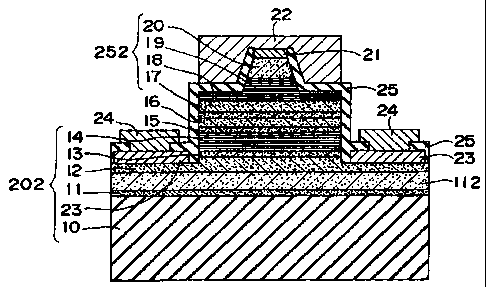
Fig. 2 is a schematic cross sectional view (cross section
perpendicular to the direction of propagation of laser light)
showing the configuration of a nitride semiconductor device
according to the second embodiment of the present invention. The
nitride semiconductor device is, for example, a nitride
semiconductor laser diode device which has an active layer 16
comprising a nitride semiconductor interposed by a semiconductor
region 202 of n conductivity side (consisting of an n-side contact
layer 12, a crack preventing layer 13, an n-side cladding layer
14 and an n-side optical waveguide layer 15) and a semiconductor
region 252 of p conductivity side (consisting of a cap layer 17,
a p-side optical waveguide layer 18, a p-side cladding layer 19
and a p-side contact layer 20) provided on a C plane of a substrate
10 made of sapphire or the like.
In the nitride semiconductor device of the second
embodiment, threshold voltage of the nitride semiconductor device
which is a laser diode is set to a low level by forming the n-side
41
CA 02276335 1999-06-29
cladding layer 14 in the semiconductor region 202 of n conductivity
side in the form of super lattice layer and forming the p-side
cladding layer 19 in the semiconductor region 252 of p conductivity
side in the form of super lattice layer. The nitride semiconductor
device according to the second embodiment of the present invention
will be described in detail below by referring to Fig. 2.
In the nitride semiconductor device of the second
embodiment, first the n-side contact layer 12 is formed on the
substrate 10 via a buffer layer 11 and a second buffer layer 112,
then the crack preventing layer 13, the n-side cladding layer 14
and the n-side optical waveguide layer 15 are laminated on the
n-side contact layer 12, thereby to form the semiconductor region
202 of n conductivity side. Formed on the surfaces of the n-side
contact layer 12 exposed on both sides of the crack preventing
layer 13 are n-side electrodes 23 which make ohmic contact with
the n-side contact layer 12, while an n-side pad electrode for
the purpose of wire bonding, for example, is formed on the n-
side electrode 23. Then the active layer 16 made of a nitride
semiconductor is formed on the n-side optical waveguide layer 15,
and the cap layer 17, the p-side optical waveguide layer 18, the
p-side cladding layer 19 and the p-side contact layer 20 are formed
on the active layer 16, thereby to form the semiconductor region
252 of p conductivity side . Further on the p-side contact layer
20, the p-side electrode 21 which makes ohmic contact with the
p-side contact layer 20 is formed, and the p-side pad electrode
for the purpose of wire bonding, for example, is formed on the
42
CA 02276335 1999-06-29
p-side electrode 21. Formed on the p-side contact layer 20 and
the p-side cladding layer 19 is a ridge which extends long in the
direction of resonance, thereby to trap light in the active layer
l6.in the transverse direction (direction perpendicular to the
direction of propagation) and form a resonator which resonates
in the longitudinal direction of the ridge by using a cleavage
plane which is at right angles to the ridge, thus making the laser
oscillate.
Components of the nitride semiconductor device of the
second embodiment will now be described below.
(Substrate 10)
The substrate 10 may be made of, in addition to sapphire
having principal plane in C plane, sapphire having principal plane
in Rplane orAplane, insulating substrate such as spinel (MgA120g) ,
or other semiconductor substrate such as SiC (including 6H, 4H
and 3C), ZnS, ZnO, GaAs and GaN.
(Buffer layer 11)
The buffer layer 11 is formed by growing A1N, GaN, AlGaN,
InGaN, etc., for example, at a temperature within 900°C to a
thickness of several tens to several hundreds of angstroms. While
the buffer layer 11 is formed for the purpose of relaxing lattice
constant mismatch between the substrate and the nitride
semiconductor, it may be omitted depending on the method of growing
the nitride semiconductor, type of substrate and other conditions .
(Second buffer layer 112)
The second buffer layer 112 is a layer made of a single
43
CA 02276335 1999-06-29
crystal nitride semiconductor which is grown on the buffer layer
11 at a temperature higher than that of the buffer layer, and is
formed to be thicker than the buffer layer 11. The second buffer
layer 112 is made as a layer which has a concentration of n-type
impurity lower than that of the n-side contact layer 12 to be grown
next, or as a nitride semiconductor layer which is not doped with
an n-type impurity. The second buffer layer 112 may be constituted
as InXAlYGaI_X_YN ( 0 ~ X, 0 5 Y, X+Y < 1 ) , for example, of which
composition is not a matter of importance here, but the composition
is preferably in the form of AlYGaI_YN which is undoped and has a
proportion of A1 (value of Y) within 0.1, and most preferably
undoped GaN. When made in such a composition, the second buffer
layer 112 having few defects can be grown and, when the second
buffer layer 112 is made in the form of undoped GaN, the second
buffer layer 112 having fewest defects can be formed. Also it is
further preferable that the n-side contact layer 12 be formed in
super lattice structure.
When the second buffer layer 112 having low impurity
concentration and few defects is grown before growing the n-side
contact layer 12, as described above, the n-side contact~layer
12 having a high carrier concentration and few defects can be formed
with a relatively larger thickness. That is, while the n-side
contact layer 12 having a high carrier concentration needs to be
formed by growing a nitride semiconductor of a high n-type impurity
concentration, it is difficult to grow a thick nitride
semiconductor layer having a high impurity concentration with few
44
CA 02276335 2003-O1-07
defects. Thus when the n-side contact layer 12 is formed without
forming the n-side buffer layer 112, not only the n-side contact
layer 12 having many defects is formed but also other nitride
semiconductor such as active layer comes to be grown on the n-side
contact layer having many defects, causing the layer to be formed
thereon to include crystal defect extending from the layer below,
making it impossible for the layer (active layer or the like) to
be formed thereon to grow with few defects. Therefore, the second
buffer layer 112 has important roles in growing the n-side contact
layer to be formed thereon with few defects as well as in forming
the semiconductor layers which constitute the nitride
semiconductor device with few defect.
Thickness of the second buffer layer 112 is preferably
controlled to be 0.1 ~.un or greater, more preferably 0.5 ~.un or greater,
and most preferably in a range from 1 dun to 20 um. When the second
buffer layer 112 is thinner than 0.1 ~.un, substantial improvement
in the crystal quality of the n-side contact layer 12 cannot
be expected. When the second buffer layer 112 is thicker than 20
~.un, on the other hand, the second buffer layer 112 itself tends
to include many crystal defects resulting in decreased effect of
buffer layer. When the second buffer layer 112 is grown to be
relatively thick to an extent that does not exceed 20 ~.un, there
is an advantage of improved heat dissipation. That is, when a laser
device is made, heat is more easily transmitted in the second buffer
layer 112 and therefore life of the laser device is elongated.
Moreover, leaking light from the laser light diffuses in the second
CA 02276335 2003-O1-07
buffer layer 112, thereby making it easier to obtain a laser beam
having near ellipticalconfiguration. The second buffer layer 112
may be omitted when an electrically conductive substrate such as
GaN, SiC, Zn0 or the like is used as the substrate.
(n-side contact layer 12)
The n-side contact layer 12 acts as a contact layer whereon
a negative electrode is formed, of which thickness is preferably
controlled within a range from 0.2 ~.tm to 4 ~.un. When the thickness
is less than 0.2 um, it becomes difficult to control the etching
rate for exposing the layer in a subsequent process of forming
the negative electrode. When the thickness is greater than 4 ~.un,
on the other hand, crystal quality tend to become poorer due
to impurity. The n-side contact layer 12 is made of, for example,
GaN doped with Si. Doping concentration of n-type impurity in the
nitride semiconductor of the n-side contact layer 12 is preferably
in a range from 1 X 101'/cm3 to 1 X 10²¹/cm3, and more preferably from
1 X 10¹⁸/cm3 to 1 X 101'/cm' . When the concentration is lower than 1
X 101'/cm3, satisfactory ohmic contact with the n electrode material
cannot be obtained and therefore threshold current and voltage
cannot be decreased in a laser device. When the concentration is
higher than 1 X 10²¹/cm3, leak current in the device increases and
the crystal quality deteriorates, resulting in a shorter device
life. It is desirable to set the impurity concentration in the
n-side contact layer 12 higher than that of the n-cladding layer
14 thereby to increase the carrier concentration in the n-side
contact layer 12, in order to reduce the ohmic contact resistance
46
CA 02276335 2003-O1-07
with the n electrode 23. When an electrically conductive
substrate such as GaN, SiC, Zn0 or the like is used as the substrate
and the negative electrode is installed on the back of the substrate,
the n-side contact layer 12 acts as a buffer layer, not as a contact
layer.
At least one of the second buffer layer 11 and the n-
side contact layer 12 may also be made in super lattice structure,
in which case crystal quality of the layer are drastically
improved and the threshold current can be decreased. Preferably
the n-side contact layer 12 which is thinner than the second buffer
layer 11 is made in super lattice structure. When the n-side
contact layer 12 is made in such a super lattice structure that
the first layer and the second layer having different levels of
band gap energy are laminated, contact resistance with the n
electrode 23 can be decreased and the threshold value can be
decreased by exposing the layer having lower band gap energy
thereby to form the n electrode 23. As materials to make the n
electrode 23 for providing favorable ohmic contact with the n-type
nitride semiconductor, there are metals such as Al, Ti, W, Si,
Zn, Sn and In, and alloys thereof.
When the n-side contact layer 12 is made in super lattice
structure of different impurity concentration, resistance in the
transverse direction can be reduced due to an effect similar to
that of HEMT described in conjunction with the first embodiment,
thereby making it possible to reduce the threshold voltage and
current of the LD device.
47
CA 02276335 2003-O1-07
(Crack preventing layer 13)
The crack preventing layer 13 is made of, for example,
Ino,lGao,9N doped with Si in a concentration of 5X101e/cm3 and has
a thickness of, for example, 500 angstroms . The crack preventing
layer 13, when formed by growing an n-type nitride semiconductor
which includes In, preferably InGaN, is capable of preventing
cracks from developing in a nitride semiconductor layer which
includes A1 to be formed thereon. The crack preventing layer 13
is preferably grown to, a thickness in a range from 100 angstroms
to 0.5 um. When the thickness is less than 100 angstroms, the layer
does not function well as a crack preventing layer. When the
thickness is greater than 0. 5 um, the crystal tends to be blackened.
The crack preventing layer 13 may be omitted when the n-side
contact layer 12 is made in super lattice structure as in the case
of the first embodiment, or when the n-side cladding layer 14 to
be grown next is made in super lattice structure.
(n-side cladding layer 14 made in n-type super lattice structure)
The n-side cladding layer is made of n-type Alo.2Gao,8N doped
with Si in a concentration of 5 X 10¹⁸/cm3 in super lattice structure
made by laminating the first layer 20 angstroms thick and the second
layer made of undoped GaN 20 angstroms thick alternately, and has
an overall thickness of, for example, 0.5 um. The n-side cladding
layer 14 functions as a carrier trapping layer and light trapping
layer and, when it is made in super lattice structure, one of the
layers is preferably made by growing a nitride semiconductor which
includes Al, preferably AlGaN. When the layer is grown to a
48
CA 02276335 2003-O1-07
thickness not less than 100 angstroms and within 2 dun, more
preferably in a range from 500 angstroms to 1 pm, a good carrier
trapping layer can be formed. While the n-side cladding layer 14
may be made by growing a single nitride semiconductor, it may also
be made in a super lattice layer which enables it to form a carrier
trapping layer of good quality of crystal without cracks.
(n-side optical waveguide layer 15)
The n-side optical waveguide layer 15 is made of, for
example, n-type GaN doped with Si in a concentration of 5 X 10¹⁸/cm'
and has a thickness of 0.1 um. The n-side optical waveguide layer
functions as an optical waveguide layer for the active layer
and is preferably formed by growing GaN or InGaN to a thickness
usually in a range from 100 angstroms to 5 ~.un, more preferably
in a range from 200 angstroms to 1 ~.un. The optical waveguide layer
1 5 15 may also be made in super lattice structure. In the case when the n-
side
optical waveguide layer 15 and the n-side cladding layer 14 are
made in super lattice structure, mean band gap energy of the nitride
semiconductor layers which constitute the super lattice layer is
set to be higher than that of the active layer. When forming a
super lattice layer, at least one of the first layer and the second
layer may or may not be doped with an n-type impurity. The n-
side optical waveguide layer 15 may also be either a single layer
of undoped nitride semiconductor or a super lattice layer made
by laminating undoped nitride semiconductors.
(Active layer 16)
The active layer 16 is made by alternately laminating a
49
CA 02276335 2003-O1-07
quantum well layer which is made of, for example, Ino.2Gao.8N doped
with Si in a concentration of 8X10¹⁸/cm' and has a thickness of
25 angstroms and a barrier layer made of Ino,osGao.9sN doped with Si
in a concentration of 8 X 10¹⁸/cm3 and has a thickness of 50 angstroms,
thereby forming a layer of multiple quantum well structure (MQW)
having a specified thickness. In the active layer 16, either both
or one of the quantum well layer and the barrier layer may be doped
with the impurity. When doped with an n-type impurity, threshold
value tends to decrease. When the active layer 16 is made in
multiple quantum well structure as described above, it is always
formed by laminating the quantum well layer having a lower band
gap energy and a barrier layer having a band gap energy lower than
that of the quantum well layer, and is therefore distinguished
from super lattice layer.. Thickness of the quantum well layer is
within 100 angstroms, preferably within 70 angstroms and most
preferably 50 angstroms . Thickness of the barrier layer is within
150 angstroms, preferably within100 angstroms and most preferably
70 angstroms. For example, the quantum well structure active
layer disclosed by Japanese Non-examined Patent Publication No.
9-148678.
(p-side cap layer 17)
The p-side cap layer 17 has band gap energy higher than
that of the active layer 16, and is made of, for example, p-type
Alo,3Gao,,N doped with Mg in a concentration of 1 X 10²°cm3 and
has
a thickness of, for example, 200 angstroms. While the cap layer
17 is preferably used in this way according to the second embodiment,
CA 02276335 1999-06-29
the cap layer is formed with a small thickness and therefore may
be of i-type wherein carriers are compensated by doping n-type
impurity. Thickness of the p-side cap layer 17 is controlled
within 0.1 um, more preferably within 500 angstroms, and most
preferably within 300 angstroms. When grown to a thickness
greater than 0.1 u.m, cracks tend to develop in the p-side cap layer
17 making it difficult to grow a nitride semiconductor layer of
good quality of crystal . When the thickness of the p-side cap layer
17 is greater than 0.1 um, the carrier cannot pass through the
p-side cap layer 17, which acts as an energy barrier, through tunnel
effect. When the penetration of carrier by tunnel effect is taken
into consideration, the thickness is preferably set to within 500
angstroms and more preferably within 300 angstroms.
The p-side cap layer 17 is preferably formed by usingAlGaN
having a high proportion of A1 in order to make the LD device easier
to oscillate, and the LD device becomes easier to oscillate when
the AlGaN layer is made thinner. For example, in the case of
AlYGaI_YN with the value of Y being 0.2 or greater, the thickness
is preferably controlled within 500 angstroms. While the lower
limit of the p-side cap layer 17 is not specified, it is preferably
formed to a thickness not less than 10 angstroms.
(p-side optical waveguide layer 18)
The p-side optical waveguide layer 18 has band gap energy
higher than that of the p-side cap layer 17 and is made of, for
example, p-type GaN doped with Mg in a concentration of 1 X 10z°/cm'
and has a thickness of 0.1 elm. The p-side optical waveguide layer
51
CA 02276335 2003-O1-07
18 functions as an optical waveguide layer for the active layer
16, and is preferably formed by growing GaN, InGaN similarly to
the n-side optical waveguide layer 15. This layer functions also
as .a buffer layer when growing the p-side cladding layer 19, and
functions as a favorable optical waveguide layer when grown to
a thickness in a range from 100 angstroms to 5 dun, and more
preferably in a range from 200 angstroms to 1 dun. While the p-side
optical waveguide layer is usually rendered p-type conductivity
by doping a p-type impurity such as Mg, alternatively it may not
be doped with any impurity. And the p-side optical waveguide layer
may also be made in super lattice structure . When made in super
lattice structure, at least one of the first layer and the second
layer may be doped with a p-type impurity, or may not be doped
at all.
(p-side cladding layer 19 = super lattice layer)
The p-side cladding layer 19 is made of p-type Al°,2Ga°,eN
doped with Mg in a concentration of 1 X 10²°/cm3 in super lattice
structure made by alternately laminating the first layer 20
angstroms thick and the second layer which is made of p-type GaN
and is doped with Mg in a concentration of 1 X10²°/cm3 having a
thickness of 20 angstroms. The p-side cladding layer 19 functions
as a carrier trapping layer similarly to the n-side cladding layer
14 and particularly functions as a layer for decreasing the
resistivity of the p-type layer. While limits of thickness of the
p-side cladding layer 19 are not specified, it is preferably
formed to a thickness not less than 100 angstroms and not greater
52
CA 02276335 1999-06-29
than 2 m, more preferably not less than 500 angstroms and not
greater than 1 um.
(p-side contact layer 20)
The p-side contact layer 20 is made of, for example, p-type
GaN doped with Mg in a concentration of 2 X lOZ°/cm' and has a
thickness of, for example, 150 angstroms. The p-side contact
layer 20 can be made in a constitution of InXAlYGaI_X_YN (O~X, 0
SY, X+Y<1) of p-type, and the most preferable ohmic contact with
the p electrode 21 can, be obtained by using GaN doped with Mg as
described above. Thickness of the p-type contact layer is
preferably controlled to within 500 angstroms, more preferably
within 300 angstroms and most preferably within 200 angstroms.
This is because resistivity can be further decreased by controlling
the thickness of the p-type nitride semiconductor which has a high
resistivity of several ohm-centimeters or higher within 500
angstroms, thus reducing the threshold current and voltage. It
is also made possible to increase the amount of hydrogen removed
from the p-type layer, thereby further reducing the resistivity.
According to the present invention, the p-side contact
layer 20 may also be made in super lattice structure. When making
a super lattice layer, the first layer and the second layer having
different values of band gap energy are laminated in a succession
of 1st, 2nd, 1st, 2nd and so on, so that the layer having lower
band gap energy is exposed at the last, in which case preferable
ohmic contact with the p electrode 21 can be obtained. The p
electrode 21 may be made of, for example, Ni, Pd, Ni/Au, etc.
53
CA 02276335 2003-O1-07
According to the second embodiment, an insulating film
25 made of SiOz is formed on the surface of nitride semiconductor
layer exposed between the p electrode 21 and an n electrode 23
as.shown in Fig. 2, while the p pad electrode 22 which is
electrically connected to the p electrode 21 via an aperture formed
in the insulating film 25 and an n pad electrode 24 connected to
the n electrode 23 are formed. The p pad electrode 22 increases
the substantial surface of the p pad electrode 22 so that the side
of p electrode can be wire-bonded and die-bonded, and the n pad
electrode 24 prevents the n electrode 23 from peeling off.
The nitride semiconductor device of the second embodiment
has the p-type cladding layer 19 of good crystal quality which
is a super lattice layer made by laminating the first layer and
the second layer with a film thickness within the elastic strain
limit. With this configuration of the nitride semiconductor
device according to the second embodiment, resistance of the p-side
cladding layer I9 can be decreased to a level at least one order
of magnitude lower than that of a p-type cladding layer which does
not have super lattice structure, and therefore threshold voltage
and current can be reduced.
Also in the nitride semiconductor device of the second
embodiment, a nitride semiconductor having a low band gap energy
is formed as the p-side contact layer 20 having a small thickness
of 500 angstroms or less in contact with the p-side cladding layer
19 which includes p-type AlYGaI_YN, so that the carrier
concentration of the p-side contact layer 20 is substantially
54
CA 02276335 2003-O1-07
increased and favorable ohmic contact with the p electrode can
be obtained, thereby making it possible to decrease the threshold
current and voltage of the device. Further, because the second
buffer layer 112 is installed before growing the n contact layer,
the nitride semiconductor layer to be grown on the second buffer
layer 112 can render good crystal quality and a long-
life device can be made. When the n-side contact layer which is
grown on the second buffer layer 112 is made in super lattice
structure, resistance in the transverse direction is reduced
thereby making it possible to make a device having low threshold
voltage and threshold current.
In the case when a nitride semiconductor which includes at least
indium, such as InGaN, is provided in the active layer 16 in the
LD device of the second embodiment 2, it is preferable that a super
lattice layer made by alternately laminating InxGal_XN and AlYGaI_YN
is used as layers which interpose the active layer 16 (the n-
side cladding layer 14 and the p-side cladding layer 19). When
configured in this way, differences in the band gap energy and
refractive index between the active layer 16 and the super lattice
layer can be increased, so that the super lattice layer can act
as an excellent light trapping layer when a laser device is
manufactured. Moreover, because InGaN has softer crystal
characteristics than other nitride semiconductors which include
A1 such as AlGaN, cracks are less likely to develop throughout
the laminated nitride semiconductor layers when InGaN is used in
the active layer. Thus the service life of the LD device can be
CA 02276335 2003-O1-07
lengthened.
In the case of a semiconductor device of double-hetero
structure having the active layer 16 of quantum well structure
as .in the second embodiment, it is preferable that the p-side cap
layer 17 made of a nitride semiconductor which has band gap energy
higher than that of the active layer 16 and a thickness within
0.1 um, preferably the p-side cap layer 17 made of a nitride
semiconductor which includes A1 is installed in contact with the
active layer 16, the p-side optical waveguide layer 18 having a
band gap energy lower than that of the p-side cap layer 17 is
installed at a position farther than the p-side cap layer 17 from
the active layer, and a nitride semiconductor having a band gap
energy higher than that of the p-side optical waveguide layer 18,
preferably the p-side cladding layer 19 having super lattice
structure which includes a nitride semiconductor including A1,
is installed at a position farther than the p-side optical
waveguide layer 18 from the active layer. Because the p-side cap
layer 17 is made with a high band gap energy, electrons inj ected
from the n layer are blocked by the p-side cap layer 17 and trapped,
so that the electrons do not overflow the active layer, thus
resulting in less current leakage in the device.
While configurations of the nitride semiconductor device
according to the second embodiment which are preferable as the
configuration of laser device are described above, the present
invention is not limited to any particular device configuration
and is applicable as long as at least one n-type super lattice
56
CA 02276335 2003-O1-07
layer is provided in the semiconductor region 202 on n conductivity
side below the active layer 16, and at least one p-type super
lattice layer is provided in the semiconductor region 252 on p
conductivity side above the active layer 16. However, it is most
preferable for the purpose of reducing the values of Vf and
threshold of the device, that the p-type super lattice layer is
formed in the p-side cladding layer 19, which acts as a carrier
trapping layer, when provided in the semiconductor region 252 on
p conductivity side, and is formed in the n contact layer 12, which
acts as a current inj ection layer which the n electrode 23 is in
contact with, or the n cladding layer 14, which acts as a carrier
trapping layer, when provided in the semiconductor region 202 on
n conductivity side. It is a matter of course that the
configuration similar to that of the device of the second
embodiment can be applied to an LED device (except that a ridge
is not necessary for the LED device).
In the nitride semiconductor device of the second
embodiment configured as described above, it is preferable that
the device be annealed in an atmosphere which does not include
H, for example nitrogen atmosphere, at a temperature not lower
than 400°C, for example 700°C, after the layers have been
formed.
This process decreases the resistance of each layer of the p-
type nitride semiconductor region further, thereby decreasing the
threshold voltage further.
Also in the nitride semiconductor device of the second
embodiment, the p electrode 21 made of Ni and Au is formed in the
57
CA 02276335 2003-O1-07
form of stripe on the surface of the p-side contact layer 12, while
the n-side contact layer is exposed symmetrically with respect
to the p electrode 21 and the n electrode 23 is installed to cover
nearly the entire surface of the n-side contact layer. When an
insulating substrate is used, such a configuration of providing
the n electrode 23 symmetrically on both sides of the p electrode
21 is very advantageous to decrease the threshold voltage.
According to the second embodiment, a multi-layer
dielectric film made of Si02 and Ti02 may be formed on the cleavage
plane (plane of resonator) which is perpendicular to the ridge
(stripe-shaped electrode).
According to the present invention, because the super
lattice layer is used either as the cladding layer which acts as
the carrier trapping layer formed in the n-type region or p-type
region interposing the active layer, or as an optical waveguide
layer of the active layer or as a current inj ection layer provided
with an electrode being formed in contact therewith, it is
preferable to control the mean band gap energy of the nitride
semiconductor which constitutes the super lattice layer to be
higher than that of the active layer.
Embodiment 3
Fig. 3 is a schematic cross sectional view showing the
configuration of the nitride semiconductor device according to
the third embodiment of the present invention. The nitride
semiconductor device of the third embodiment is a laser diode of
stripe electrode type using the end face of the active layer as
58
CA 02276335 2003-O1-07
a resonance plane, and Fig. 3 schematically shows the cross section
of the device when cut in a direction perpendicular to the direction
of propagation of laser light. The third embodiment of the present
invention will be described below by referring to Fig. 3.
In Fig. 3, reference numerals refer to the following
components.
100 denotes a GaN substrate of a thickness not less than
um which is grown on an auxiliary substrate made of a material
other than nitride semiconductor, for example a substrate made
10 of such material as sapphire, spinel, SiC, Si, GaAs and ZnO. The
auxiliary substrate may be removed after the GaN substrate 100
is formed as shown in Fig. 3, or may be left to remain thereon
and used without removal as in the case of an embodiment to be
described later (Fig. 8).
11 denotes a buffer layer made of Si-doped n-type GaN,
which also functions as an n-side contact layer in the third
embodiment.
14 denotes an n-side cladding layer of super lattice
structure made by laminating Si-doped n-type Alo,2Gaa,8N (first
nitride semiconductor layer) 40 angstroms thick and undoped GaN
layer (second nitride semiconductor layer) 40 angstroms thick,
alternately in 100 layers. In the third embodiment, the n-side
cladding layer 14 is formed at a position located apart from the
active layer.
15 denotes an n-side guide layer made of, for example,
undoped GaN which is placed between the n-side cladding layer 14
59
CA 02276335 1999-06-29
and the active layer 16 and has a band gap energy lower than that
of Alo.ZGao,BN of the n-side cladding layer 14.
A semiconductor region 203 of n conductivity side is
constituted from the n-side buffer layer 11, the n-side cladding
layer 14 and the n-side optical waveguide layer 15.
16 denotes an active layer of multi-quantum well structure
made by laminating three quantum well layers made of Alo,2Gao,8N with
a thickness of 30 angstroms and two barrier layers made of
Ino,os~ao.9sN having a band gap energy higher than that of the quantum
well layers and thickness of 30 angstroms, alternately, in five
layers iri all.
17 denotes a p-side cap layer made of, for example,
Mg-doped p-type Alo,3Gao,,N which has a band gap energy higher than
the band gap energy of the quantum well layers of the active layer
16 and higher than the band gap energy of the p-side optical
waveguide layer 18. The band gap energy of the p-side cap layer
17 is preferably set to be higher than that of the nitride
semiconductor layer (fourth nitride semiconductor layer) which
has less band gap energy among the p-side cladding layer 19 of
the super lattice structure.
18 denotes the p-side guide layer made of, for example,
undoped GaN which is placed between the p-side cladding layer 19
and the active layer 16 and has a band gap energy lower than that
of Alo.ZGao,BN of the p-side cladding layer 19.
19 denotes a p-side cladding layer of super lattice
structure made by laminating Mg-doped p-type Alo,2Gao,8N which is
CA 02276335 2003-O1-07
40 angstroms thick and undoped GaN layer 40 angstroms thick,
alternately in 100 layers, located apart from the active layer.
20 denotes a p-side contact layer made of, for example,
Mg-doped GaN which has a band gap energy lower than that of the
Alo,2Gao,8N of the p-side cladding layer 19.
A semiconductor region 253 of p conductivity side is
constituted from the p-side cap layer 17, the p-side optical
waveguide layer 18, the p-side cladding layer 19 and the p-side
contact layer 20.
As described above, the laser device of the third
embodiment of the present invention has a structure such that the
nitride semiconductor layers 11 and 14 through 20 are laminated
on the GaN substrate 100, wherein a stripe ridge is formed on the
nitride semiconductorlayerlocated over the p-side claddinglayer
19 and the p electrode 21 is formed on substantially the entire
surface of the p-side contact layer 20 located on the outermost
surface of the ridge. On the surface (top surface) of the exposed
n-side buffer layer 11, on.the other hand, is formed the n electrode
23. In the third embodiment, the n electrode 23 is formed on the
surface of the n-side buffer layer 11, but because the GaN substrate
100 is used as the substrate, such a configuration may also be
employed as the portion where the n electrode is to be formed is
etched down to the GaN substrate 100 thereby to expose the surface
of the GaN substrate 100, then the n electrode is formed on the
exposed GaN substrate 100 so that the p electrode and the n
electrode are provided on the same side. An insulating film 25
61
CA 02276335 1999-06-29
made of, for example, Si02 is formed on the exposed surface of the
nitride semiconductor except for the top of the n electrode 23
and the p electrode 21, while the n pad electrode 22 and the n
pad electrode 24 are provided for the purpose of bonding for the
connection with the p electrode 21 and the n electrode 23 via the
apertures in the insulating film 25 above the n electrode 23 and
the p electrode 21. While the region comprising the nitride
semiconductor layers placed between the active layer and the p
electrode is referred to as the semiconductor region of p
conductivity side, this does not mean that all the nitride
semiconductor layers constituting the semiconductor region have
p-type conductivity. Similarly, the region comprising the
nitride semiconductor layers placed between the active layer and
a GaN substrate 100 is referred to as the semiconductor region
of n-side conductivity, this does not mean that all the nitride
semiconductor layers constituting the region have n-type
conductivity, as described previously.
The laser device according to the third embodiment of the
present invention has the n-side cladding layer 14 of super lattice
structure made bylaminating the first nitride semiconductorlayer
having a high band gap energy and the second nitride semiconductor
layer having a band gap energy lower than that of the first nitride
semiconductor layer, the two layers having different impurity
concentrations, provided at positions apart from the active layer
16 in the n-side nitride semiconductor layer located below the
active layer 16 shown in Fig. 3. Thickness of the first nitride
62
CA 02276335 2003-O1-07
semiconductor layer and the second nitride semiconductor layer
which constitute the super lattice layer is preferably controlled
to be within.100 angstroms, more preferably within 70 angstroms
and most preferably within a range from 10 to 40 angstroms. When
the thickness is greater than 100 angstroms, the first nitride
semiconductor layer and the second nitride semiconductor layer
become thicker than the elastic strain limit and microscopic cracks
or crystal defects tend to develop in the film. While the lower
limit of the thickness of the first nitride semiconductor layer
and the second nitride semiconductor layer is not specified
according to the present invention and may be of any value as long
as it is a monoatomic layer or thicker, it is preferably 10 angstroms
or greater. Further, the first nitride semiconductor layer is
preferably made by growing a nitride semiconductor which includes
at least Al, preferably AlxGa1_XN (0<X s 1) . While the second
nitride semiconductor layer may be anything as long as it is a
nitride semiconductor having a band gap energy lower than that
of the first nitride semiconductor layer, it is preferably made
of a nitride semiconductor of binary mixed crystal or ternary mixed
crystal such as AlYGal_YN (OSY<1, X>Y) and InZGaI_ZN (OSz<1) which
can be grown easily and provide good crystal quality. According
to the present invention, it is more preferable that the first
nitride semiconductor be AlXGaI_XN (0<X<1) which does not include
In and the second nitride semiconductor be InZGaI_ZN (05Z<1) which
does not include Al, and most preferably the first nitride
semiconductor is AlXGa1_XN ( 0<X~ 0 . 3 ) with the mixing proportion
63
CA 02276335 2003-O1-07
of A1 (value of Y) being 0.3 or less and the second nitride
semiconductor is GaN, for the purpose of obtaining super lattice
of excellent crystal quality.
When the first nitride semiconductor is made by using
,5 AlXGal_XN ( 0<X<1 ) and the second nitride semiconductor is made by
using GaN, a remarkable advantage in terms of manufacture as
described below can be obtained. That is, when forming the AlXGa1_XN
(0<X<1) layer and the GaN layer by metal organic vapor phase
deposition process (MOVPE: metal organic vapor phase epitaxy),
every layer can be grown in the same HZ atmosphere. Therefore,
a super lattice layer can be formed by growing the AlXGa1_XN ( 0<X<1 )
layer and the GaN layer alternately without changing the atmosphere.
This provides a remarkable advantage when manufacturing the super
lattice layer which requires several tens to several hundreds of
layers to be laminated.
The cladding layer which has the functions of light
trapping layer and carrier trapping layer must have a band gap
energy higher than that of quantum well structure of the active
layer. Although a nitride semiconductor of high mixing proportion
of A1 can be used to make a nitride semiconductor layer of a
relatively high band gap energy, it has been very difficult to
grow a crystal of nitride semiconductor of high mixing proportion
of Al, because of cracks which are likely to develop in a thick
film. When formed in a super lattice layer as in the case of the
present invention, however, cracks are made less likely to occur
because the crystal is grown to a thickness within the elastic
64
CA 02276335 2003-O1-07
strain limit, even when the AlGaN layer formed as the first nitride
semiconductor layer constituting the super lattice layer is made
with a somewhat high mixing proportion of Al. With this
configuration, in the present invention, a layer having a high
mixing proportion of A1 can be grown with good crystal quality,
and therefore it is made possible to form a cladding layer having
good effects of light trapping and carrier trapping, thereby
reducing the threshold voltage in the laser device . The present
invention can also be applied to LED devices, in which case it
is made possible to decrease Vf ( forward voltage ) in the LED device .
Further in the laser device according to the third
embodiment of the present invention, n-type impurity
concentration is set to be different between the first nitride
semiconductor layer and the second nitride semiconductor layer
of the n-side cladding layer 14. This configuration is the
so-called modulation doping. When one layer is made with lower
n-type impurity concentration or is preferably undoped with the
impurity and the other layer is doped in a higher concentration,
this modulation doping is also capable of decreasing the threshold
voltage and Vf. This is because the presence of a layer having
a low impurity concentration in the super lattice layer increases
the mobility in the layer, and coexistence of a layer having a
high concentration of impurity makes it possible to form a super
lattice layer even when the carrier concentration is high. That
is, it is supposed that the coexistence of a layer of low impurity
concentration and high mobility and a layer of high impurity
CA 02276335 1999-06-29
concentration and high carrier concentration allows a layer having
a high impurity concentration and high mobility to be a cladding
layer, thus decreasing the threshold voltage and vf.
When a nitride semiconductor layer having a high band gap
energy is doped with an impurity in a high concentration, the
modulation doping effect is supposed to generate two dimensional
electron gas between a high impurity concentration layer and a
low impurity concentration layer, so that the resistivity
decreases due to the effect of the two dimensional electron gas.
In a super lattice layer made by laminating a nitride semiconductor
layer which is doped with an n-type impurity and has a high band
gap energy and an undoped nitride semiconductor layer with a low
band gap energy, for example, the barrier layer side is depleted
in the hetero-junction interface between the layer which is doped
with the n impurity and the undoped layer, while electrons (two
dimensional electron gas) accumulate in the vicinity of the
interface on the side of the layer having lower band gap. Since
the two dimensional electron gas is formed on the lower band gap
side and therefore the electron movement is not subject to
disturbance by the impurity, electron mobility in the super lattice
increases and the resistivity decreases. It is also supposed that
the modulation doping on p side is caused by the effect of the
two dimensional positive hole gas. In the case of p layer, AlGaN
has higher resistivity than GaN has. Thus it is supposed that,
because the resistivity is decreased by doping AlGaN with p type
impurity in a higher concentration, a substantial decrease is
66
CA 02276335 1999-06-29
caused in the resistivity of the super lattice layer, thereby
making it possible to decrease the threshold value when the laser
device is made.
When a nitride semiconductor layer having a low band gap
energy is doped with an impurity in a high concentration, such
an effect as described below is expected to be produced. When the
AlGaN layer and the GaN layer are doped with the same amounts of
Mg, for example, acceptor level of Mg becomes deeper and the
activation ratio becomes lower in the AlGaN layer. In the GaN layer,
on the other hand, acceptor level of Mg becomes less deep and the
Mg activation ratio becomes higher than in the AlGaN layer. When
doped with Mg in a concentration of 1 X 10z°/cm3, for example, carrier
concentration of about 1X10¹⁸/cm3 is obtained in GaN, while the
concentration obtained in AlGaN is only about 1 X 101'/cm3. Hence
in the present invention, a super lattice layer is made from AlGaN
and GaN and the GaN layer from which higher carrier concentration
can be expected is doped with greater amount of impurity, thereby
forming super lattice of a high carrier concentration. Moreover,
because tunnel effect causes the carrier to move through the AlGaN
layer of a lower impurity concentration due to the super lattice
structure, the carrier can move in the AlGaN layer under almost
no influence of the impurity, while the AlGaN layer functions also
as a cladding layer having a high band gap energy. Therefore, even
when the nitride semiconductor layer of lower band gap energy is
doped with a greater amount of impurity, very good effect can be
obtained in decreasing the threshold voltage of the laser device
67
CA 02276335 1999-06-29
or LED device. The above description deals with a case of forming
the super lattice layer on p-type layer side, although similar
effect can be obtained also when a super lattice layer is formed
on the n layer side.
When the first nitride semiconductor layer having a higher
band gap energy is doped with an n-type impurity in a high
concentration, the amount of doping in the first nitride
semiconductor layer is preferably controlled within a range from
1 X 1p1'/cm3 to 1 X 10²°/cm', or more preferably within a range from
1 X 10¹⁸/cm' to 5 X l Olg/cm' . When the impurity concentration is lower
than 1 X 101'/cm3, the difference from the concentration in the
second nitride semiconductor layer becomes too small to obtain
a layer of high carrier concentration. When the impurity
concentration is higher than 1 X lOz°/cm3, on the other hand, leak
current in the device itself tends to increase. Meanwhile the
n-type impurity concentration in the second nitride semiconductor
layer may be at any level as long as it is lower than that of the
first nitride semiconductor layer, but it is preferably lower than
one tenth of the latter. Most preferably the second nitride
semiconductor layer is undoped, in which case a layer of the highest
mobility can be obtained. However, because each of the component
layers of a super lattice layer is thin, some of the n-type impurity
diffuses from the first nitride semiconductor into the second
semiconductor layer. Though even in this case, effects of the
present invention can be obtained when the n-type impurity
concentration in the second nitride semiconductor layer is within
68
CA 02276335 2003-O1-07
1 X 101'/cm3. The n-type impurity is selected from among the
elements of NB group and VIB group of the periodic table such as
Si, Ge, Se, S and 0, and preferably selected from among Si, Ge
and S. The effect is the same also in the case when the
first nitride semiconductor layer having a higher band gap
energy is doped with a lesser amount of n-type impurity and
the second nitride semiconductor layer having a lower band
gap energy is doped with a greater amount of N-type impurity.
The laser device according to the third embodiment of the
present invention has the p-side cladding layer 19 of super lattice
structure made by laminating a third nitride semiconductor layer
having a high band gap energy and a fourth nitride semiconductor
layer having a band gap energy lower than that of the third nitride
semiconductor layer, the two layers having different impurity
concentrations, provided at positions apart from the active layer
16 in the p-side nitride semiconductor layer located above the
active layer 16 shown in Fig. 3. Thickness of the third nitride
semiconductor layer and the fourth nitride semiconductor layer
which constitute the super latticelayer are preferably controlled
to be within 100 angstroms, more preferably within ?0 angstroms
and most preferably within a range from 10 to 40 angstroms, as
in the case of the n-side cladding layer 14. Similarly, the third
nitride semiconductor layer is preferably made by growing a nitride
semiconductor which includes at least Al, preferably AlXGa1_XN (0
<X51) . The fourth nitride semiconductor is preferably made of
a nitride semiconductor of binary mixed crystal or ternary mixed
69
CA 02276335 2003-O1-07
crystal such as AlYGal_YN ( 05 Y<1, X>Y ) or InZGaI_ZN ( 0 s Z ~ 1 ) .
When the p-type cladding layer 19 is made in super
lattice structure, the super lattice structure has the same effect
on the laser device as that of the n cladding layer 14, and also
has such an effect as follows in addition to the case of forming
on the n layer side. That is, the p-type nitride semiconductor
has resistivity which is usually at least two orders of magnitude
higher compared to n-type nitride semiconductor. Therefore, when
a super lattice layer is formed on the p layer side, remarkable
effect of reducing the threshold voltage is obtained. Nitride
semiconductor is known to be a semiconductor which is difficult
to obtain in the form of p-type crystal. Such a process has been
known where a nitride semiconductor layer doped with a p-type
impurity is annealed and then hydrogen is removed thereby
manufacturing a p-type crystal (Japanese Patent No. 2540791).
However, the p-type nitride semiconductor thus obtained has
resistivity as high as several ohm-centimeters at the lowest. By
turning this p-type layer into a super lattice layer, better
crystal quality can be obtained and the resistivity can be
reduced at least one order of magnitude lower than that of the
prior art, thereby making it possible to decrease the threshold
voltage.
In the third embodiment, the third nitride semiconductor
layer and the fourth nitride semiconductor layer of the p-type
cladding layer 19 are set to have different concentrations of
p-type impurity, so that one layer has a high impurity
CA 02276335 2003-O1-07
concentration and the other layer has a lower impurity
concentration. Similarly to the case of the n-side cladding layer
14, threshold voltage and Vf can be decreased by doping the third
nitride semiconductor layer which has a high band gap energy with
the p-type impurity in a higher concentration and doping the fourth
nitride semiconductor layer which has a low band gap energy with
the p-type impurity in a lower concentration.
A configuration reverse to the above is also possible:
the third nitride semiconductor layer which has high band gap
energy is doped with the p-type impurity in a lower concentration
and the fourth nitride semiconductor layer which has low band gap
energy is doped with the p-type impurity in a higher concentration.
The reason is as described previously.
The amount of doping in the third nitride semiconductor
layer is preferably controlled within a range from 1 X 101e/cm3 to
1 X 10²¹/cm3, or more preferably within a range from 1 X lOl9/cm3 to
5 X 10²°/cm'. When the impurity concentration is lower than 1 X
1018/cm3, the difference from the concentration in ~ the fourth
nitride semiconductor layer becomes too small to obtain a layer
of high carrier concentration. When the impurity concentration
is higher than 1 X 10²¹/cm', on the other hand, crystal quality
tends to deteriorate. Meanwhile the p-type impurity concentration
in the fourth nitride semiconductor layer may be at any level as
long as it is lower than that of the third nitride semiconductor
layer, but it is preferably lower than one tenth of the latter.
Most preferably the fourth nitride semiconductor layer is undoped,
71
CA 02276335 2003-O1-07
in order to obtain the highest mobility. In practice, however,
because the film is thin, some of the p-type impurity diffuses
from the third nitride semiconductor. In order to obtain good
effect in the present invention, the concentration is preferably
within 1 X 10²°/cm3. The p-type impurity is selected from among the
elements of IIA group and IIB group of the periodic table such as
Mg, Zn, Ca and Be, and preferably selected from among Mg and Ca.
The above applies also to such a case as the third nitride
semiconductor layer having higher band gap energy is doped
with a lesser amount of p-type impurity and the fourth
nitride semiconductor layer having lower band gap energy is
doped with a greater amount of p-type impurity.
In the nitride semiconductor layer constituting the super
lattice layer, the layer doped with the impurity in a higher
concentration is preferably doped so that such a distribution of
impurity concentration is obtained, that the impurity
concentration is high in the middle portion of the semiconductor
layer in the direction of thickness (located far from the second
nitride semiconductor layer or the fourth nitride semiconductor
layer) and is low (or undoped) in the portions near the ends
(portions adjacent to the second nitride semiconductor layer and
the fourth nitride semiconductor layer). When the super lattice
layer is formed from the AlGaN layer doped with Si as n-type
impurity and the undoped GaN layer, the AlGaN layer releases
electrons as donor into the conductive band because it is doped
with Si, the electrons fall in the conductive band of the GaN which
72
i
CA 02276335 2003-O1-07
has a low potential. Because the GaN crystal is not doped with
the donor impurity, carrier disturbance due to an impurity does
not occur. Thus the electrons can move easily in the GaN crystal,
namely high electron mobility is obtained. This is similar to the
effect of the two dimensional electron gas described previously,
thus increasing the mobility of the electrons substantially in
the transverse direction and decreasing the resistivity. In the
AlGaN layer having a high band gap energy, the effect is further
enhanced when the central region apart from the GaN
layer is doped with the n-type impurity in a high concentration.
That is, among the electrons that move in GaN, electrons passing
through a portion near the AlGaN are more or less subject to
disturbance by the n-type impurity ions (Si in this case) which
are present in a portion of the AlGaN layer adjacent to the GaN
layer. However, when a portion of the AlGaN layer adjacent to the
GaN layer is undoped as described above, electrons passing through
the portion near the AIGaN layer become less subject to the
disturbance of Si, and therefore mobility in the undoped GaN layer
is further improved. Similar effect is obtained also when super
lattice is formed from the third nitride semiconductor layer of
the p layer side and the fourth nitride semiconductor layer,
although the action is different somewhat, and it is preferable
that the third nitride semiconductor layer having a high band gap
energy be doped with the p-type impurity in a higher concentration
at the middle portion thereof and doped in a lower concentration
or undoped at all at portions which are adjacent to the fourth
73
CA 02276335 2003-O1-07
nitride semiconductorlayer. Although theimpurity concentration
distribution may also be realized in the nitride semiconductor
layer having a low band gap energy doped with the n-type impurity
in a higher concentration, a super lattice layer made by doping
the nitride semiconductor layer of a lower band gap energy has
less effect.
While the configurations where the n-side cladding layer
14 and the p-side cladding layer 19 are made in super lattice layer
structure have been described above, accordif~g to the present
invention, the n-side buffer layer 11 acting as a contact layer,
the n-side optical waveguide layer 15, p-side cap layer 17, the
p-side optical waveguide layer 18, p-side contact layer 20, or
the like may also be formed in super lattice structure. That is,
any layer, whether it makes contact with the activation or not,
may be formed in super lattice structure. When the n-side buffer
layer 11 whereon the n electrode is formed is prepared in super
lattice structure, in particular, the effect similar to that of
HEMT can be easily obtained.
Further in the laser device according to the third
embodiment of the present invention, the n-side optical waveguide
layer 15 in which the impurity (n-type impurity in this case)
concentration is controlled within 1 X 10¹⁹/cm' is formed between
the n-side cladding layer 1~4 made of super lattice layer and the
active layer 16, as shown in Fig. 3. Even when the n-side optical
waveguide layer 15 is undoped, there is a possibility that the
n-type impurity from other layers diffuses into this layer,
74
CA 02276335 1999-06-29
although the effect of the present invention will not be lost
provided that the concentration of the doped impurity is within
1X10¹⁹/cm3, in which case the n-side optical waveguide layer 15
functions as an optical waveguide layer. However, according to
the present invention, impurity concentration in the n-side
optical waveguide layer 15 is preferably within 1 X 10¹⁸/cm3, more
preferably within 1 X 101'/cm3, and most preferably the n-side
optical waveguide layer 15 is undoped. It is also preferable that
the n-side optical waveguide layer 15 be formed from a nitride
semiconductor which includes In or from GaN.
Also in the laser device according to the third embodiment,
the p-side optical waveguide layer 18 in which the impurity (p-type
impurity in this case) concentration is controlled within 1 X
1019/cm3 is formed between the p-side cladding layer 19 made of super
lattice layer and the active layer 16. According to the present
invention, impurity concentration in the p-side optical waveguide
layer 18 may be within 1 X 10¹⁹/cm3, but is preferably controlled
within 1 X 10¹⁸/cm3 and most preferably the p-side optical waveguide
layer 18 is undoped. While a nitride semiconductor shows n-type
conductivity when undoped, conductivity of the p-side optical
waveguide layer 18 may be either n-type or p-type according to
the present invention and is referred to as p-side optical
waveguide layer regardless of the conductivity type in this
specification. In practice, there is a possibility that the
p-type impurity from other layers diffuses into the p-side optical
waveguide layer 18. It is preferable that the p-side optical
CA 02276335 1999-06-29
waveguide layer be also formed from a nitride semiconductor which
includes In or from GaN.
The reason why it is preferable that an undoped nitride
semiconductor be interposed between the active layer and the
cladding layer is as follows . A nitride semiconductor is designed
to have the active layer emit light of wavelength usually in a
range from 360 to 520 nm, more particularly from 380 to 450 nm.
An undoped nitride semiconductor has lower absorptance for light
of the wavelength region described above, than nitride
semiconductors doped with n-type impurity or p-type impurity.
Therefore, when an undoped nitride semiconductor is interposed
between a light emitting active layer and a cladding layer which
acts as a light trapping layer, light emitted by the active layer
is subject to less attenuation and it is made possible to make
a laser device which oscillates with a low gain while decreasing
the threshold voltage. This effect can be achieved when the
impurity concentration in the optical waveguide layer is within
1X10¹⁹~cm3.
Thus a preferred embodiment of the present invention is
a light emitting device which is located apart from an active layer
and has a cladding layer of super lattice structure that has been
modulation-doped with an impurity, and a guide layer which is doped
with an impurity in a low concentration or preferably undoped,
interposed between the cladding layer and the active layer.
Further preferred embodiment is the light emitting device
of the third embodiment wherein a quantum well layer of active
76
CA 02276335 2003-O1-07
layer and the p-side cap layer 17 made of a nitride semiconductor
of thickness 0.1 um or less having a band gap energy higher than
the band gap energy of the interface of the p-side guide layer
18 is formed between the p-side guide layer 18 and the active layer
16, with the impurity concentration in the p-side cap layer being
controlled at 1 X lOle/cm3 or higher. Thickness of the p-type cap
layer 17 is controlled within 0.1 ~,un, more preferably within 500
angstroms, and most preferably within 300 angstroms. When grown
to be thicker than 0.1 pm, cracks tend to develop in the p-type
cap layer 17 thus making it difficult to grow a nitride
semiconductor layer of good crystal quality. When a thin layer
having a high band gap energy is formed to a thickness within 0.1
um adj acent to the active layer, leak current in the light emitting
device can be decreased. This causes the electrons injected from
the n layer side to accumulate in the active layer due to the energy
barrier of the cap layer, resulting in increased probability of
recombination of electrons and positive holes, thereby making it
possible to increase the output power of the device. It is
necessary to control the impurity concentration in the cap layer
at 1 X lOle/cm3 or higher. That is, the cap layer has a relatively
high proportion of mixed Al, and a layer having a high proportion
of mixed A1 tends to have high resistance. Therefore, unless the
layer is doped with an impurity to increase the carrier
concentration and reduce the resistivity, the layer becomes
similar to i layer of high resistance, thus forming p-i-n structure
with poor current-voltage characteristics. The cap layer
77'
CA 02276335 1999-06-29
provided on the p side may also be formed on the n side. When formed
on the n side, doping of the n-type impurity is not necessary.
In the laser device of the third embodiment constituted
as described above, because the n-side cladding layer 14 and the
p-side cladding layer 19 are made in super lattice structure,
electric resistance and the threshold voltage of the n-side
cladding layer 14 and the p-side cladding layer 19 can be reduced
and the laser can be oscillated for a long period of time.
In the laser device of the third embodiment, reduction
of the threshold voltage is attempted with various means as
described above, in addition to the constitution of the n-side
cladding layer 14 and the p-side cladding layer 19 in super lattice
structure.
Although the n-side cladding layer 14 and the p-side
cladding layer 19 are made in super lattice structure in the third
embodiment, the present invention is not limited to this
configuration and either one of the n-side cladding layer 14 and
the p-side cladding layer 19 may be made in super lattice structure .
With such a configuration, too, the threshold voltage can be
reduced compared to the prior art.
Although the n-side cladding layer 14 and the p-side
cladding layer 19 are made in super lattice structure in the third
embodiment, the present invention is not limited to this
configuration and it suffices that any one or more of the p-side
and n-side nitride semiconductor layers other than the n-side
cladding layer 14 and the p-side cladding layer 19 may be made
78
CA 02276335 1999-06-29
in super lattice structure. With such a configuration, too, the
threshold voltage can be reduced compared to the prior art.
Although the n-side cladding layer 14 and the p-side
cladding layer 19 are made in super lattice structure in the laser
device of the third embodiment, the present invention is not
limited to this configuration and can be applied to other nitride
semiconductor devices such as light emitting diode (LED), as a
matter of course. With such a configuration, Vf (forward voltage)
can be reduced in the, case of a light emitting diode.
As described above, because the laser device of the third
embodiment has the cladding layer made in super lattice layer made
by modulation doping of an impurity, the threshold voltage can
be decreased and oscillation can be continued for a long period
of time. Also the laser device can be set to a high characteristic
temperature which makes it possible to make a good laser device.
The characteristic temperature is the threshold current density
as a function of temperature, which is proportional to exp (T/To) ,
where T is the operating temperature (K) and To is the
characteristic temperature (K) . In the laser device, higher value
of To allows lower threshold current density even at a: high
temperature, resulting in stable operation. In the laser device
of embodiment 27 to be described later, for example, To is as high
as 150K or over. This value indicates excellent temperature
characteristic of the LD. Thus when the laser device of the present
invention is used as a writing light source and/or reading light
source, a capacity not obtained with the prior art can be achieved,
79
CA 02276335 2003-O1-07
providing great industrial utilization value.
Embodiment 4
Fig. 9 is a schematic perspective view showing the shape
of the laser device according to the fourth embodiment of the
present invention. Fig. 9 also shows the cross section of the device
when cut in a direction perpendicular to the ridge stripe. The
fourth embodiment of the present invention will be described below
by referring to Fig. 9.
Each layer of the laser device according to the fourth
embodiment is formed in a manner as described below.
(Underlying layer 302)
The underlying layer 302 is, for example, made of GaN
and has a thickness of 4 ~.un. The underlying layer 302 is formed
via a 200-angstrom-thick buffer layer (not shown) consisting of
GaN on an auxiliary substrate 301 made of, for example, sapphire.
The underlying layer 302 partially forms a protective film on the
surface and is used for the layer on which the nitride semiconductor
substrate is to be selectively grown. The underlying layer 302
is made of GaN or AlxGa1_XN and when it includes A1, AlxGa1_xN
(O~XS0.5) having an Al mixed crystal ratio exceeds 0.5, cracking
easily occurs in the crystal itself, rather than the crystal
defects, resulting in difficult crystal growth.
The underlying layer 302 is desirably grown to a larger thickness
than that of the buffer layer and adjusted to not more than 10
um. The auxiliary substrate 301 may be made of SiC, ZnO, spinel,
GaAs and the like, as well as sapphire, which are known to be used
CA 02276335 2003-O1-07
for growing nitride semiconductors and are different from
nitride semiconductors.
(Protective film 303)
For a protective film 303, 1-um-thick SiOz film having
a sufficient length in the resonating direction is patterned to
form 10-um-wide stripe windows with a periodicity of 2 ~.un on the
underlying layer 302. The examples of the protective film may
include stripes, dots or checks. The protective film 303 may
preferably have a larger area than the windows (the exposed parts
of the underlying layer 302 on which the Si02 is not formed), so
as to grow a nitride semiconductor substrate 304 with fewer crystal
defects. The materials of the protective film 303 may include
oxides such as silicon oxide (SiOx), silicon nitride (SixNiY),.
titanium oxide (TiOX) and zirconium oxide (ZrOX), nitrides, or
multi-layer film thereof, as well as metals having a melting point
higher than 1200°C. These materials can withstand high temperatures
ranging between 600°C and 1100°C at which nitride semiconductors
can be grown and nitride semiconductors do not grow or are difficult
to grow on the surface of the materials.
(Nitride semiconductor substrate 304)
For a nitride semiconductor substrate 304, for example,
undoped GaN having a thickness of, for example, 20 dun is grown
on the protective film 303 using MOVPE method. The nitride
semiconductor substrate 304 may be grown using Halide Vapor Phase
Epitaxy (HYPE) method as well as using MOVPE method in this way.
The nitride semiconductor substrate may be most preferably
81
i
CA 02276335 2003-O1-07
obtained by growing GaN without In or A1. It is most desirable
to use TMG as well as organic gallium compounds such as
triethylgallium (TEG) as a gas for growth and to use ammonia or
hydrazine as nitrogen sources. Donor impurities such as Si and
Ge may be doped to the GaN substrate so as to adjust the carrier
density to a suitable range. In the case where the auxiliary
substrate 301, the underlying layer 302, and the protective film
303 are eliminated, the nitride semiconductor substrate functions
as a contact layer and therefore, donor impurities may be desirably
doped to the nitride semiconductor substrate.
(n-side buffer layer 311= which also functions as a contact layer)
The n-side buffer layer 311 is obtained , for example,
by forming a 5 ~.m-thick GaN doped with Si to 3 X 10¹⁸/cm' on the
nitride semiconductor substrate 304. The buffer layer 311
functions as a contact layer for forming a n-electrode in the case
of the fabrication of the light emitting device having a structure
as shown in Fig. 9. In the case where the auxiliary substrate 301
to the protective film 303 are eliminated and the electrode is
formed on the nitride semiconductor substrate 304, the n-side
buffer layer can be omitted. The n-side buffer layer 311 is one
which is grown at high temperature and is different from the buffer
layer which is formed by growing GaN, A1N and the like to a thickness
of 0.5 pm or less directly on the substrate of the material such
as sapphire, SiC and spinel and which is different from the nitride
semiconductor at a low temperature of 900°C or less.
82
CA 02276335 2003-O1-07
(Crack-preventing layer 312)
The crack-preventing layer 312 is formed by, for example,
growing Ino.a6Gaa.e,N to a thickness of 0.15 um on the n-side buffer
layer 311.
(n-side cladding layer 313 = super lattice layer)
The n-side cladding layer 313 is composed of a super
lattice layer which is obtained by alternately laminating the
25-angstrom-thick first layer consisting of .n-type A1o,16Gao.e,N
doped with Si to 1 X 10'e~cm' and the 25-angstrom-thick second layer
consisting of undoped GaN, and has a total thickness of, for example,
1.2 dun. The n-side cladding layer 313 composed of a super lattice
layer has an average A1 composition of 8.0 ~ and the product of
that and the film thickness equals 9. 6. In the case where the n-side
cladding layer 313 is composed of a super lattice layer obtained
by laminating the nitride semiconductor layers which have
different band gap energy from each other, more impurities may
be doped to one layer, that is, modulation-doping may be performed,
so as to lower the threshold value . The composition and thickness
of the n-side cladding layer 313 (a super lattice layer) will be
described in detail below.
(n-side light waveguide layer 314)
The n-side light waveguide layer 314 is made of undoped GaN
and has a thickness of, for example, 0.1 ~.un. The n-side light
waveguide layer functions as a light waveguide layer for the active
layer. The n-side light waveguide layer is desirably formed by
growing GaN or InGaN to a thickness, usually ranging between 100
angstroms and 5 um, preferably ranging between 200 angstroms and
83
CA 02276335 1999-06-29
1 elm .
(active layer 315)
The active layer 315 is made by alternately laminating
a quantum well layer which is made of undoped In°.ZGa°.8N and
has
a thickness of 40 angstroms and a barrier layer made of undoped
Ino.o~Ga°.99N and has a thickness of 100 angstroms, thereby
forming
a layer of multiple quantum well structure having a total thickness
of, for example, 440 angstroms. The active layer 315 may be undoped
as in the present embodiment or may be doped with donor impurities
and/or p-type impurities . In this case, either both or one of the
quantum well layer and the barrier layer may be doped with the
impurity.
(p-side cap layer 316)
The p-side cap layer 316 has band gap energy higher than
that of the p-side light waveguide layer 317 which is formed thereon,
and is made of p-type Al°,3Ga°,,N doped with Mg in a
concentration
of 1 X 10²°/cm3 and has a thickness of, for example, 300 angstroms .
The p-type cap layer 316 has a thickness of 0.1 ~.un or less so as
to enhance the laser of the device. The lower limit of the film
thickness is not specified, but the p-side cap layer 316=may
desirably have a thickness of 10 angstroms or more.
(p-side light waveguide layer 317)
The p-side light wave guide layer 317 has band gap energy
lower than that of the p-side cap layer 316, and is made of, for
example, undoped GaN and has a thickness of 0.1 Vim. The p-side
light waveguide layer functions as a light waveguide layer for
84
CA 02276335 2003-O1-07
the active layer and is desirably made of GaN or InGaN like the
n-type light waveguide layer 314.
(p-side cladding layer 318)
The p-side cladding layer 318 has a super lattice
structure made by alternately laminating the third layer which
is made of p-type Al°.l6Ga°.a4N doped with Mg to 1 X
102°/cm3 and has
a thickness of 25 angstroms and the fourth layer which is made
of undoped GaN and has a thickness of 25 angstroms. The p-side
cladding layer 318 has an average A1 composition of 8~ and the
product of the value and the film thickness equals 4.8. In the
case that the p-side cladding layer 318 is composed of a super
lattice layer obtained by laminating the nitride semiconductor
layers at least one of which includes a nitride semiconductor layer
containing A1 and which have different band gap energy from each
other, more impurities may be doped to any one layer, that is,
modulation-doping may be performed, so as to lower the threshold
value. The composition and thickness of the p-side cladding layer
318 (a super lattice layer) will be described in detail below.
Now, the thickness of the core part (waveguide part)
which is sandwiched between the cladding layers will be described
below. The core part is the area including the n-side light
waveguide layer 314, active layer 315, p-side cap layer 316 and
the p-side light waveguide layer 317, that is, the nitride
semiconductor layers including the active layer which are
sandwiched between the n-side cladding layer and the p-side
cladding layer and the area in which waveguides emit from
CA 02276335 2003-O1-07
the active layer. In the case of the nitride semiconductor laser
device, as mentioned above, FFP is not a single beam because the
emission leaking via the cladding layer can be wave-guided within
the n-side contact layer, resulting in multi-mode. Otherwise, the
emission resonates within the core part, resulting in multi-mode.
According to the present invention, the n-side cladding layer has
a large thickness and a large average A1 composition in order to
obtain the difference between the refractive indices and to trap
the emission from the core part within the cladding layer. However,
if the multi-mode occurs within the core part, FFP is disturbed.
Therefore, in order that the multi-mode does not occur within the
core part, the thickness of the core part is desirably adjusted,
with respect to the n-side cladding layer. The thickness is
desirably adjusted to the range from 200 angstrom to 1.0 dun,
preferably from 500 angstroms to 0.8 ~.un, most preferably from 0.1
dam to 0.5 dun, in order that the multi-mode does not occur within
the core part. If the thickness is below 200 angstroms, the
emission leaks from the core part to increase the threshold value.
If the thickness is above 1.0 dun, the multi-mode is likely to occur.
(p-side contact layer 319)
The p-side contact layer 319 is made of, for example,
p-type GaN doped with Mg to 2 X 10²°/cm3 and has a thickness of, for
example, 150 angstrom. The p-side contact layer 319 can be made
in a constitution of p-type InxAlYGaI_X_YN(OSX, O~Y, X-~Y~1), as
well as p-type GaN as mentioned above, and the preferable ohmic
contact with the p electrode 321 can be obtained by using GaN doped
86
CA 02276335 2003-O1-07
with Mg.
In the embodiment 4, the wafer on which each nitride
semiconductor layer is formed is preferably annealed at 700°C
within the nitrogen atmosphere in the reactor , so as to decrease
the resistance of the layer doped with the p-type impurity.
In the laser device of the embodiment 4, the p-side
contact layer 318 which is a top layer, and the p-side cladding
layer are etched with the RIE apparatus to form a ridge geometry
having a stripe width of 4 dun, as shown in Fig. 9. When the ridge
stripe is formed, the ridge stripe is formed above the position
of the surface of the nitride semiconductor substrate 304 where
the crystal defects do not appear. In Fig. 9, the crystal defects
appear in the central part of the protective film 303 in the form
of a stripe and in the central part of the window in the form of a
stripe . Thus, when the stripe is formed at the point where almost
no crystal defects are present, the crystal is prevented from
developing to the active layer, with the result that the laser
device has a long lifetime and the reliability thereof can
be enhanced.
Further, a mask is formed on the ridge surface and the
etching is performed with RIE to expose the surface of the n-
side buffer layer 311 on both sides of the ridge. On the exposed
surface of the n-side buffer layer 311, the n electrode 322 made
of Ti and A1 is formed, respectively.
And on the outermost surface of the ridge of the A-
side contact layer 319, the p electrode 320 made of Ni and Au is
87
CA 02276335 2003-O1-07
formed in the form of a stripe. As shown in Fig. 9, the insulating
film 323 made of Si02 is formed on the surface of the nitride
semiconductor layer which is exposed between the p electrode 320
and the n electrode 322. The p-pad electrode 321 which is
electrically connected to the p electrode 320 is formed via the
insulating film 323.
The sapphire substrate of the wafer on which the n
electrode and p electrode are formed in a manner as mentioned above
is polished to a thickness of 70 pna and cleaved into bars from
the substrate, perpendicularly with respect to the stripe-shaped
electrode to fabricate a resonator in which the cleaving facet
functions as a reflective plane. A multi-layer dielectric film
made of Si02 and TiOz may be formed on the reflective plane.
The laser device of the fourth embodiment is fabricated
as described above.
The laser device of the embodiment 4 fabricated as
descibed above has as a light trapping layer the n-side cladding
layer 313 and the p-side cladding layer 318 of a super lattice
structure which have smaller refractive indices than the well layer
of the active layer and include nitride semiconductor,
respectively. In the embodiment 4, the super lattice layer means
the multi-layer structure obtained by laminating nitride
semiconductor layers which have a thickness of not more than 100
angstroms respectively and have a different composition from each
other. The thickness of the layer which is laminated is preferably
not more than 70 angstroms, and more preferably not more than 40
88
CA 02276335 2003-O1-07
angstroms. To be concrete, for example, the super lattice layer
may be made by laminating the layer made of AlXGa1_XN(0<X<1) and
the other nitride semiconductor layer which has a different
composition from the layer made of AlXGa1_xN, and by laminating the
layer of the ternary mixed crystal and the layer of the ternary
mixed crystal or the layer of the ternary mixed crystal and the
layer of binary mixed crystal such as AlXGa1_XN/GaN,
AlXGal-xN/AlYGal_YN (0<Y<1, Y<X) , AlXGa1_xN /InZGal_ZN (0<Z<1) and so on.
Thereamong, the most preferable super lattice layer is made of
AlxGa1_xN and GaN.
Next, the total thickness of the n-side cladding layer
313 and the thickness and the composition of each layer which
constitute the super lattice layer according to the embodiment
4 will be described.
First, in these specifications, the A1 average
composition of the super lattice layer means that calculated as
described below. For example, when the super lattice layer is made
by laminating a 25-angstrom-thick Alo.SGao.SN and a 25-angstrom-
thick GaN in 200 pairs ( 1. 0 ~.un) , the thickness of one pair is 50
angstroms and the mixing proportion of A1 of the layer containing
A1 is 0 . 5 . Using the value 0 .25 obtained by multiplying the mixing
ratio of A1 of the layer containing Al, 0.5, by the film thickness
ratio (25/50), the A1 average composition of the super lattice
layer is 25$.
When the super lattice layer is made by laminating the
layers having a different thickness, that is, by laminating a
89
CA 02276335 2003-O1-07
40-angstrom-thick Alo,SGao.SN and a 20-angstrom-thick GaN, the
weighted mean of the film thickness is calculated to be 0.5 (40/60)
- 0.33, and therefore, the A1 average composition is 33.3. That
is, the mixing ratio of Al of the nitride semiconductor layer
containing Al multiplied by the ratio of said nitride semiconductor
layer to one pair of the super lattice layers equals the A1 average
composition in the present invention. When both layers contain
Al, the A1 average composition can be obtained in the same manner.
For example, the super lattice layer is made by laminating a
20-angstrom- thick Alo_lGao.eN and a 30-angstrom-thick Alo.2Gao_8N,
0.1 (20/50) + 0.2 (30/50) - 0.16, that is, the A1 average
composition is 16~. The example mentioned above refers to
AlGaN/GaN and AlGaN/AlGaN and the same calculation method can be
applied to the case of AlGaN/InGaN. And, the A1 average
composition of the n-side cladding layer can be detected with an
instrument for analysis such as SIMS (secondary ion mass
spectrometer) and Auger electron spectrometer.
In the embodiment 4, the composition and the film
thickness of each layer which constitute the super lattice layer
of the n-side cladding layer 313 is set on the basis of the A1
average composition as calculated using the above-mentioned
calculating method. The laser device according to the embodiment
4 is characterized in that the total thickness of the n-side
cladding layer 313 is not less than 0.5 dun and the Al average
composition in ~ of the n-side cladding layer 313 is set to be
such that the product of the A1 average composition (~) multiplied
CA 02276335 2003-O1-07
by the total thickness of the n-side cladding layer (dam) is not
less than 4.4. In other words, in the embodiment 4, the thickness
and the A1 average composition of each layer constituting the super
lattice layer are set to be such that the total thickness of the
n-side cladding layer 313 is not less than 0.5 um and the product
of said thickness multiplied by the A1 average composition in $
as calculated in the above-mentioned way is not less than 4.4.
When the total thickness of the n-side cladding layer
313 is less than 0.5 dun and the product of said total thickness
(dun) multiplied by the A1 average composition (~) is less than
4.4, the light trapping effect of the n-side cladding layer is
insufficient and the resonance occurs again in the n-side contact
layer, with the result that the FFP is disturbed and the threshold
value tends to increase . The product of the Al average composition
multiplied by the total thickness of the n-side cladding layer
313 is preferably not less than 5.0, more preferably not less than
5.4, most preferably not less than 7Ø
According to the present invention, because of the
n-side cladding layer 313 composed of a super lattice layer, even
if the mixing ratio of Al is increased, the cracks can be difficult
to develop in the cladding layer. Therefore, the upper limit of
the total thickness of the n-side cladding layer 313 is not
specified from the viewpoint of crystallinity (from the viewpoint
in which the cracks are prevented from occurring), and however,
it is desirable to control the thickness to be not more than 5
um so as to decrease the laminating times of the nitride
91
CA 02276335 1999-06-29
semiconductor layers which constitute the super lattice layer.
To be concrete, for example, the total thickness of said
n-side cladding layer is set to be not less than 0.8 dun and the
A1 average composition which is contained in said n-side cladding
layer is set to be not less than 5. 5 ~ . In this case, the product
is not less than 4.4. Preferably, the total thickness of said
n-side cladding layer is set to be not less than 1.0 elm and the
A1 average composition which is contained in said n-side cladding
layer is set to be not less than 5. 0 ~ . In this case, the product
is not less than 5. 0. More preferably, the total thickness of said
n-side cladding layer is set to be not less than 1.2 um and the
A1 average composition which is contained in said n-side cladding
layer is set to be not less than 4 . 5 ~ . In this case, the product
is not less than 5.4. The examples mentioned above described
concretely the relation between the thickness of the n-side
cladding layer and the A1 average composition of the n-side
cladding layer made in super lattice structure. It is known that
when the mixing ratio of A1 in AlXGa1_XN is increased, the band gap
energy increases and the refractive index decreases. Therefore,
it is ideal and industrially convenient that the AlXGa1_xN layer
having a large mixing ratio of A1 of, for example, not less than
0.5 is grown in a single layer of, for example, a few um, however,
the AlXGa1_XN layer is difficult to be grown thickly. If the AlXGa1_XN,
particularly having a mixing ratio of A1 of not less than 0.5,
is intended to be grown in a single layer, the cracks should develop
in the crystal in the thickness of, for example, not less than
92
CA 02276335 2003-O1-07
0.1 um. Thus, the AlXGa1_XN layer having a mixing ratio of A1 of
not less than 0.5 is difficult to be grown in a single layer having
a thickness of, for example, a few um.
However, according to the present invention, a thin film
made of AlXGa1_XN is used to constitute a super lattice layer and
the thickness of the single film is not more than the critical
film thickness of AlXGa1_xN, therefore, the cracks being to develop.
Therefore, when the cladding layer is composed of a super lattice
layer, the layer having'a high mixing ratio of A1 and a large
thickness can be grown. In the present invention, since the
relation between the specific mixing ratio of A1 and the thickness
of the cladding layer could be found, the combination thereof
enables the light not to leak from the n-side cladding layer to
the substrate side.
When the n-side cladding layer is constituted as
mentioned above to trap the emission from the active layer, the
p-side cladding layer may have the same constitution as that of
the n-side cladding layer. When the p-side cladding layer 318 is
constituted in the same manner as the n-side cladding layer 313,
the thickness of the p-side cladding layer is desirably smaller
than that of the n-side cladding layer. Because, when the mixing
ratio of A1 or the thickness of the p-side cladding layer is large,
the resistance of the AlGaN layer tends to increase with the result
that the threshold value tends to increase. Therefore, even if
the p-side cladding layer is constituted of a super lattice layer
including the nitride semiconductor layer containing A1 and the
93
CA 02276335 1999-06-29
product of the thickness multiplied by the Al average composition
is not less than 4.4, the thickness is desirably no more than 1.0
dun. The lower limit is not specified but is desirably not less
than 50 angstroms in order to function as a cladding layer. In
the case of the super lattice layer, the A1 average composition
is desirably not more than 50 ~ . Since the p-side cladding layer
is shaped into a ridge and the electrode is installed thereon,
the leakage of the light can be almost neglected and it is not
necessary for the p-side cladding layer to have the same
constitution as that of the n-side cladding layer 313, but the
p-side cladding layer may have the same constitution as that of
the n-side cladding layer. That is, the p-side cladding layer has
a super lattice structure including the nitride semiconductor
layer containing at least A1 and has a total thickness of not more
than 1.0 dun. Moreover, the A1 average composition in ~ contained
in the p-side cladding layer may be set to be such that the product
of the total thickness (um) of the p-side cladding layer multiplied
by the A1 average composition ($) is not less than 4.4.
When the p-side cladding layer is composed of a super
lattice layer including the nitride semiconductor layer
containing A1 (in this case, the leakage of light is not concerned
and the case in which the cladding layer functions only as a carrier
trapping layer is included), the total thickness of the n-side
cladding layer is desirably larger than that of the p-side cladding
layer. The p-side cladding layer is composed of a super lattice
layer made by laminating the nitride semiconductor layers in the
94
CA 02276335 2003-O1-07
same way as the n-side cladding layer, for example, by laminating
the AlXGa1_xN (0<X<1) layer and the other nitride semiconductor
layer which has a different composition from said AlxGal_XN layer,
or by laminating the layer made of ternary mixed crystal and the
layer made of ternary mixed crystal or the layer made of ternary
mixed crystal ant the layer made of binary mixed crystal such as
AlXGa1_xN/GaN, AlXGa1_XN/AlYGaI_YN (0<Y<1, Y<X), AlXGa1_XN/Ina Gal_ZN
(0<Z<1) and so on. Thereamong, the most preferable super lattice
layer is made of AlxGa1_XN and GaN.
Examples
The invention will be described in detail in the
following examples.
Example 1
According to Example 1 of the invention, nitride
semiconductor devices (LD devices) , as shown in Fig. 1 and 2, can
befabricated. The nitride semiconductor devices were fabricated
as follows.
First, a C-plane sapphire substrate 10 was set in the
reactor and the inside atmosphere of the reactor was fully replaced
with hydrogen. The temperature of the substrate was increased to
1050°C with hydrogen. flow in order to clean the substrate.
Subsequently, the temperature was decreased to 510°C.
A first buffer layer 11 consisting of GaN was grown to a film
thickness of about 200 angstrom using hydrogen as a carrier gas,
CA 02276335 2003-O1-07
ammonia and TMG (trimethylgallium) as a source of GaN.
After growing the buffer layer, only TMG was stopped
and the temperature was increased to 1050°C. At 1050°C in the
same
way using ammonia and TMG (trimethylgallium) as a source of GaN,
a 5 ~.un-thick second buffer layer 112 consisting of undoped GaN
having a carrier density of 1 X 10¹⁸/cm3 was grown.
Subsequently, a 1 um-thick n-side contact layer 12
consisting of n-type GaN doped with Si to 1 X 10¹⁹/cm' was grown,
using TMG and ammonia and silane gas (SiH4) as a source of impurity
at 1050°C.
Next, the temperature was adjusted to 800°C. A
500-angstrom-thick crack-preventing layer consisting Ino.lGao.9N
doped with Si to 5 X 1p18/cm3 was grown, using TMG, TMI
(trimethylindium) and ammonia as source gases and silane gas as
a source of impurity.
Then, the temperature was increased to 1050°C and a
20-angstrom-thick first layer consisting of n-type Alo.2Gao,eN doped
with Si to 5 X 10¹⁸/cm' was grown, using TMA, TMG , ammonia and silane
gas. Subsequently, TMA and silane were stopped and a 20-
angstrom-thick second layer consisting of undoped GaN was grown.
Then, each of these operations was repeated 100 times and a n-side
cladding layer 14 of superlattices having a total thickness of
0 . 4 dun was grown .
Subsequently, a 0.1 ~.un-thick n-side light guide layer
15 consisting of n-type GaN doped with Si to 5 X 10¹⁸/cm' was grown
at 1050°C.
96
CA 02276335 1999-06-29
Next, an active layer 16 was grown using TMG, TMI,
ammonia and silane. For the active layer 16, first, a 25-
angstrom-thick well layer 25 consisting of In°.ZGa°.BN doped
with
Si to 8 X 10¹⁸/cm3 was grown at 800°C. Next, at the same
temperature,
a 50-angstrom-thick barrier layer consisting of
In°.°1Ga°.99N doped
with Si to 8 X 10¹⁸/cm3 was grown, only by changing the molar ratio
of TMI. This operation was repeated twice. Finally, the well
layer was laminated and a multi-quantum-well-structure active
layer 16 was grown with a total thickness of 175 angstroms.
Next, the temperature was increased to 1050°C. A
300-angstrom-thick p-side cap layer 17 consisting of p-type
Al°.3Ga°.,N doped with Mg to 1 X 10²°/cm' was grown
which had a greater
band gap energy than the active layer, using TMG, TMA and ammonia
as a source of AlGaN and Cp2Mg (cyclopentadienyl magnesium) as
a source of impurity.
Subsequently, a 0.1 um-thick p-side light guide layer
18 consisting of p-type GaN doped with Mg to 1 X 10z°/cm3 was grown
which had a smaller band gap energy than the p-side cap layer 17
at 1050°C.
Subsequently, a 20-angstrom-thick first layer
consisting of p-type Al°,zGa°,8N doped with Mg to 1 X
102°/cm3 was grown,
using TMA, TMG, ammonia and Cp2Mg at 1050°C. Subsequently, TMG
was stopped and a 20-angstrom-thick second layer consisting of
p-type GaN doped with Mg to 1 X lOZ°/cm3 was grown. Each of these
operations was repeated 100 times and a p-side cladding layer 19
of superlattices with a total thickness of 0.4 um was formed.
97
CA 02276335 2003-O1-07
Finally, a 150-angstrom-thick p-side contact layer 20
consisting of p-GaN doped with Mg to 2 X 10²o~cm3 was grown on the
p-side cladding layer 19 at 1050°C.
After the reaction was completed, the temperature was
decreased to room temperature. Additionally, the annealing was
performed to the wafer at 700°C in nitrogen atmosphere within the
reactor, so as to make the p-type layer less resistive. The
annealing method disclosed in U.S. Patent 5,306,662 is employed
in this Example.
After annealing, the wafer was removed from the reactor.
As shown in Fig. 2, the top p-side contact layer 20 and the p-side
cladding layer 19 were etched with RIE apparatus to make them a
ridge geometry having a stripe width of 4 dun.
Next, a mask was formed on the surface of the ridge.
As shown in Fig. 2, the surfaces of the n-side contact layer were
exposed symmetrically with respect to the stripe ridge.
Next, a p-electrode 21 consisting of Ni and Au was formed
on the almost whole top surface of the stripe ridge of the p-
side contact layer 20, while an n-electrode 23 consisting of Ti ;'
and A1 was formed on the almost whole surface of the stripe-geometry
n-side contact layer.
Next, as shown in Fig. 2, an insulating film 25 was formed
on the surface of the nitride semiconductor layer exposed between
p-electrode 21 and n-electrode 23. A p-pad electrode 22 and an
n-pad electrode 24 were formed which are electrically connected
to the p-electrode via the insulating film 25.
98
CA 02276335 2003-O1-07
The wafer on which the n-electrode and p-electrode were
formed in the above-mentioned manner was transferred to the
polishing machine. The sapphire substrate on whose side the
nitride semiconductor was not formed was lapped with a diamond
abrasive to a substrate thickness of 50 um. After lapping, the
surface of the substrate was further polished by 1 dun with a finer
abrasive, resulting in the mirror facet.
After polishing the substrate, the polished facet was
scribed and cleaved into bars perpendicularly with respect to the
stripe-geometry electrode to fabricate a facet of a resonator on
the cleaving facet. A dielectric multi-layer film consisting of Si02
and Ti02 was formed on the facet of the resonator and finally, the
bar was cut parallel to the p-electrode, resulting in laser chips .
Next, the chips were set face-up ( in the state that the substrate
was faced to the heat sink) onto the heat sink and each electrode
was connected by wire-bonding. The laser oscillation was tried
at room temperature. The continuous emission at an emission
wavelength of 405 nm was observed at the threshold current density
of 2 . 9 kA/cm2 and the threshold voltage of 4 .4V at room temperature.
The lifetime was 50 hours or longer.
(Comparative Example 1)
With the same procedure as in Example 1, the second
buffer layer was not grown; the 5 ~.un-thick n-side contact layer
12 only consisting of n-type GaN doped with Si to 1 X 10¹⁹/cm3 was
grown, the 0.4 ~m-thick n-side cladding layer only consisting of
n-type Alo.ZGao.BN doped with Si to 1 X 10¹⁹/cm' was grown, the 0 . 4
99
CA 02276335 1999-06-29
~.un-thick p-side cladding layer 19 only consisting of p-type
Al°.2Ga°.8N doped with Mg to 1 X 10²°/cm3 was grown,
and the 0 . 2 ~.m-thick
p-side contact layer 20 only consisting of p-type GaN doped with
Mg to 2 X 10²°/cm' was grown, so as to obtain laser devices . The
basic
construction was as shown in Fig. 1.
Table 1
Substrate 10 sapphire
Buffer layer 11 GaN 200 ~1
n-side contact layer ' Si doped n-type GaN 5 dun
12
Si:1X10¹⁹/cm'
Crack preventing layer13 Si doped n-type In,lGa.9N 500 ~
Si:5X10¹⁸/cm'
n-side cladding layer 14 Si doped n-type Al.ZGa.eN 0.5 dun
Si:5X1018cm3
n-side optical 15 Si doped n-type GaN 0.1 dun
waveguide layer Si 5 X 10¹⁸/cm3
:
Active layer (MQW) 16 Si doped In_ZGa.8N 25 ~
(total thickness 1750 Si doped In.1Ga .9sN 50 ~
S1 8 X 1~18~3
:
Cap layer 17 Mg doped p-type Al_1Ga.9N 300 ~r
Mg : 1 X 102cm3
p-side optical 18 Mg doped p-type GaN 0.1 um
waveguide layer Mg:1 X 102cm3
p-side cladding layer 19 Mg doped p-type Al_ZGa,8N 0.5 um
Mg:1 X 102cm3
p-side contact layer 20 Mg doped p-type GaN 0.2 ~.un
Mg:2 X 102cm3
100
CA 02276335 2003-O1-07
For the laser devices of Comparative Example 1
constructed in this way, the continuous emission was obtained at
the threshold current density of 7kA/cm2. However, the threshold
voltage was 8.0V or higher and the emission was observed for few
minutes.
Example 2
With the same procedure as in Example 1, for the n-side
contact layer 12, a 30-angstrom-thick first layer consisting of
n-type Alo.oSGao.9sN doped with Si to 2 X 10¹⁹/cm3 was grown and
subsequently, a 30-angstrom-thick second layer consisting of
undoped GaN was grown and these procedures were repeated, resulting
in superlattices having a total thickness of 1.2 ~.un. The other
constructions of the laser devices were the same as in Example
1. The threshold current density was 2.7kA/cm2, the threshold
voltage was 4.2V and the lifetime was 60 hours or longer.
Example 3
The laser devices were fabricated which had the same
constructions as in Example 2, except for the n-side contact layer
12 composed of superlattices whose second layers consisted of GaN
doped with Si to 1 X 101e/cm3. The laser devices had almost similar
properties to those of Example 2.
Example 4
The laser devices were fabricated which had the same
constructions as in Example 1, except that the 0.4 dun- thick second
buffer layer 112 consisting of GaN doped with Si to 1 X 10¹⁷/cm3 was
101
CA 02276335 2003-O1-07
grown. The threshold current density was 2 .9kA/cm2, the threshold
voltage was 4.5V and the lifetime was 50 hours or longer.
Example 5
With the same procedure as in Example 1, for the n-.
side contact layer 12, a 60-angstrom-thick first layer consisting
of n-type Alo,ZGao.BN doped with Si to 2 X 10¹⁹/cm' was grown and
subsequently, a 40-angstrom-thick second layer consisting of GaN
doped with Si to 1 X 101'/cm' of Si was grown and these procedures
were repeated , resulting in superlattices having a total thickness
of 2 dun. And the 0.4 ~.un-thick n-side cladding layer 14 consisting
of only n-type Alo.2Gao,8N doped with Si to 1 X 10¹⁹/cm' was grown.
The other constructions of the laser devices were the same as those
in Example 1. The threshold current density was 3.2kA/cm2, the
threshold voltage was 4.8V and the lifetime was 30 hours or longer.
Example 6
With the same procedure as in Example 1, the following
procedures (1) and (2) were changed.
(1) After the growth of the buffer layer 11, only TMG
was stopped and the temperature was increased to 105b°C. At
1050°C,
the 60-angstrom-thick first layer consisting of n-type Ala.2Gaa_BN
doped with Si to 1 X 101'/cm' was grown using TMA, TMG, ammonia and
silane as material gases and subsequently, silane and TMA were
stopped and the 60-angstrom-thick second layer consisting of
undoped GaN was grown. The superlattices were constructed in a
manner of the first layer + the second layer + the first layer
+ the second layer + "'. Five hundred first layers and five
102
CA 02276335 2003-O1-07
hundred second layers were laminated by turns . The n-side contact
layer 12 of superlattices having a total thickness of 5 ~.un was
formed.
(2 )' Next, the 500-angstrom thick-crack preventing layer
13 consisting of Ino.lGao,9N doped with Si to 5X10¹⁸/cm3 was
grown in the same manner as in Example 1.
And at 1050°C the 0.5 dun-thick n-side cladding layer
14 consisting of n-type Alo.2Gao.8N doped with Si to 5 X lOle~cm3 was
grown using TMA, TMG, ammonia and silane.
The constructions above the n-side cladding layer were
the same as those of the laser devices in Example 1. The laser
devices of this example had the basic constructions as described
in Table 1, except that the n-side contact layer 12 and p-side
cladding layer 19 were composed of superlattices and the p-side
contact layer 20 had a thickness of 150 angstrom like Example 1.
The continuous emission at a wavelength of 405nm was observed at
the threshold current density of 3.2kA/cm2 and the threshold
voltage of 4.8V. The lifetime was 30 hours or longer.
Further, in the case that the film thickness of the
p-side contact layer of LDs according to Example 6 is changed
gradually, the relation between the film thickness of the p-side
contact layer and the threshold voltage of the LDs is shown in
Fig. 5. The figure shows the threshold voltages in the case when the
p-side contact layer has a thickness of less than 10 angstrom (A) ,
10 angstrom (B) , C (30 angstrom) , 150 angstrom (D: this example) ,
500 angstrom (E) , 0.2 dun (F) , 0.5 dun (G) and 0. 8 ~.un (H) , in order
103
CA 02276335 2003-O1-07
from the left. As shown in this drawing, the threshold voltage
tends to increase gradually when the film thickness of the p-
side contact layer is over 500 angstrom. The p-side contact layer
20 preferably has a thickness of 504 angstrom or less, more
preferably 300 angstrom or less. When the film thickness is 10
angstrom or less (almost one atom layer or two atom layer), the.
surface of the p-side cladding layer 19 which is under the p-
side contact layer is exposed and therefore, the contact resistance
of the p-electrode is bad, resulting in that the threshold voltage
tends to increase. However, since LDs of the present invention
had a superlattice layer, the threshold voltage was much lower
than that of the comparative examples.
(Comparative Example 2)
The laser devices having the construction as described
in Table 1 were fabricated, except that n-side cladding layer 14
was formed which was a multi-layer film having a total thickness
of 0. 6 dun, by growing the 180-angstrom-thick first layer consisting
n-type AIo,ZGao,BN doped with Si to 1 X 10¹⁹/cm2 and subsequently,
growing the 120-angstrom-thick second layer consisting of undoped
GaN. That is, the thickness of the first layer and second layer
was increased and LDs were fabricated. The continuous emission
was observed at the threshold current density of 6.5 kA/cmz and
the threshold voltage was 7.5 V. The emission was observed for
a few minutes.
Example 7
The laser devices having the same construction as in
104
CA 02276335 2003-O1-07
Example 6 were fabricated, except that the p-side cladding .layer
19 had a superlattice structure with a total thickness of 0.5 um
obtained by laminating the 60-angstrom-thick first layers
consisting of Alo,2Gao,eN doped with Mg to 1 X 10²°/cm' and the
40-angstrom-thick second layers consisting of p-type GaN doped
with Mg to 1 X 10²°/cm3. That is, the thickness of the superlattice
layer constructing the p-side cladding layer 19 of Example 7 was
changed and the other constructions were the same as in Example
7 . The threshold voltage increased a little, as compared with that
in Example 6. The lifetime was 20 hours or longer.
Example 8
The laser devices having the same construction as in
Example 7 were fabricated, except that the n-side cladding layer
19 had a superlattice structure with a total thickness of 0.5 um
obtained by laminating the 60-angstrom-thick first layers
consisting of Al°.2Ga°.eN doped with Si to 1 X 10¹⁹/cm' and the
40-angstrom-thick second layers consisting of n-type GaN doped
with Si to 1 X 10¹⁹/CIIl3. That is, the laser devices had superlattices
as the n-side cladding layer, in addition to the n-side contact
layer and p-side cladding layer having a superlattice structure
in Example 6. The present laser devices had similar properties
to those of Example 6.
Example 9
With the same procedures as in Example l, the second
buffer layer 112 was not grown and the 5 pm-thick n-side contact
layer consisting of n-type GaN doped with Si to 1 X 101'/cm3 was grown
105
CA 02276335 2003-O1-07
directly on the first buffer layer 11. The other constructions
were the same as those in Example 1. That is, the laser devices
had the basic constructions as described in Table 1, except that
the n-side cladding layer 14 had a superlattice structure with
a total thickness of 0.4 um obtained by laminating the 20
angstrom-thick first layers consisting of n-type Al°,ZGa°,8N
doped
with Si to 1X101'/cm' and the 20-angstrom-thick second layers
consisting of undoped GaN. Further, the p-side cladding layer had
a superlattice structure with a total thickness of 0.4 dun obtained
by laminating the 20-angstrom-thick first layers consisting of
p-type Al°.2Ga°.8N doped with Mg to 1 X 10¹⁹/cm3 and the 20-
angstrom-thick second layers consisting of p-type GaN doped with
Mg to 1 X 10²°/cm3. Additionally, the p-side contact layer 20
consisted of p-type GaN doped with Mg to 2 X 10²°/cm' and had a
thickness of 15 angstrom. The continuous emission at a wavelength
of 405 nm was observed at the threshold current density of 3.3kA/cm2
and the threshold voltage was 5.0V. The lifetime was 30 hours or
longer.
Example 10
The laser devices were fabricated in the same manner
as in Example 9, except that the second layer which constructed
the superlattices of the n-side cladding layer 14 consisted of
GaN doped with Si to 1 X 101'/cm3. That is, the laser devices were
fabricated in the same manner as in Example 9, except that the
2 5 layers having a larger band gap energy were doped with Si to a larger
amount. The present laser devises had similar properties to those
106
CA 02276335 2003-O1-07
of Example 9.
Example 11
The laser devices were fabricated in the same manner
as in Example 9, except that the second layer which constructed
the n-side cladding layer 14 consisted of n-type
In°.°1Ga°,99N doped
with Si to 1X10¹⁹/cm3. That is, the laser devices were fabricated
in the same manner as in Example 9, except that the second layer
which composed the superlattices of the n-side cladding layer 14
consisted of InGaN and, had the same impurity density as the first
layer. The present laser devices had similar properties to those
of Example 9.
Example 12
With the same procedures as in Example 9, the n-side
cladding layer had a superlattice structure with a total thickness
of 0.5 a composed of the 60-angstrom-thick first layers consisting
Al°.2Ga°.8N doped with Si to 1 X 10¹⁹/cm3 and the 40-
angstrom-thick
second layers consisting of GaN doped with Si to 1X10¹⁹/cm3.
Further, the p-side cladding layer 19 had a superlattice structure
with a total thickness of 0.5u composed of the 60-angstrom-thick
first layers consisting Al°.2Ga°,eN doped with Mg to 1 X
102°/rm' and
the 40-angstrom-thick second layers consisting of GaN doped with
Mg to 1 X 10²°/cm3. That is, the laser devices were fabricated in
the same manner as in Example 9, except that the doped amounts
in the first layers and the second layers composing the n-side
cladding layer 14 were equal to each other, the thickness of them
was changed, and the thickness of the first layers and the second
107
CA 02276335 2003-O1-07
layers composing the p-side cladding layer 19 was changed. The
continuous emission at a wavelength of 405nm was observed at the
threshold current density of 3.4kA/cm2 and the threshold voltage
was 5.2V. The lifetime was 20 hours or longer.
Example 13
The laser devices having the same constructions as those
in Example 11 were fabricated, except that the second layer
composing the n-side cladding layer 14 consisted of GaN doped with
Si to 1 X101'/cm'. The. present laser devices had similar
properties to those in Example 11.
Example 14
The laser devices having the same constructions as those
in Example 11 were fabricated, except that the second layer
composing the n-side cladding layer 14 consisted of undoped GaN.
The present laser devices had the similar properties as those in
Example 11.
Example 15
The laser devices were fabricated in the same manner
as in Example 9, except that the 0.4~.un-thick n-side cladding layer
14 consisting of only n-type Al°.2Ga°,8N doped with Si to 1 X
1019/cm3
was grown. That is, the present laser devices had the basic
constructions as described in table 1, except that the p-side
cladding layer 19 had a superlattice structure with a total
thickness of 0.4 um composed of the 20-angstrom-thick first layers
consisting of p-type A10 .2Ga0. 8N doped with Mg to 1 X 10²°/cm' and
the20-angstrom-thick second layers consisting of p-type GaN doped
108
CA 02276335 1999-06-29
with Mg to 1X10¹⁹/cm3 and further, the p-side contact layer 20 had
a thickness of 150 angstroms and consisted of p-type GaN doped
with Mg to 2 X 10²°/cm3 like Example 1. The continuous emission at
a wavelength of 405 nm was observed at the threshold current density
of 3.4 kA/cm2. The threshold voltage was 5.1V and the lifetime
was 20 hours or longer.
Example 16
The laser devices were fabricated in the same manner
as in Example 15, except that the p-side cladding layer 19 had
a superlattice structure with a total thickness of 0. 5 ~.un obtained
by laminating the 60-angstrom-thick first layers (Al°.ZGa°_eN)
and
the 40-angstrom-thick second layers (GaN). The threshold voltage
tended to rise a little. The lifetime was 20 hours or longer.
Example 17
The laser devices were fabricated in the same manner
as in Example 9, except that the 0.4 ~.un-thick p-side cladding layer
19 consisting of only p-type Al°.ZGa°,8N doped with Mg to 1 X
102°/cm3
was grown. That is, the present laser devices had the basic
constructions as described in table 1, except that the n-side
cladding layer 14 had a superlattice structure with a total
thickness of 0.4 um composed of the 20-angstrom-thick first layers
consisting of p-type Al°.ZGa°.8N doped with Si to 1 X 10¹⁹/cm'
and the
20-angstrom-thick second layers consisting of undoped GaN and
further, the p-side contact layer 20 had a thickness of 150 angstrom
and consisted of p-type GaN doped with Mg to 2 X 10z°/cm3 like Example
1. The continuous emission at a wavelength of 405 nm was observed
109
CA 02276335 1999-06-29
at the threshold current density of 3.5 kA/cm2. The threshold
voltage was 5.4V and the lifetime was 20 hours or longer.
Example 18
The laser devices were fabricated in the same manner
as in Example 17, except that the n-side cladding layer 14 had
a superlattice structure with a total thickness of 0.49 um obtained
by laminating the 70-angstrom-thick first layers consisting of
Alo.2Gao.eN and the 40-angstrom-thick second layers consisting of
Ino_olgao.99N doped with .Si to 1 X 10¹⁹/cm3. The threshold voltage
tended to rise a little, compared with that in Example 16. The
lifetime was 10 hours or longer.
Example 19
The laser devices were fabricated in the same manner
as in Example 17, except that the n-side cladding layer 14 had
a superlattice structure with a total thickness of 0.5 dun obtained
by laminating the 60-angstrom-thick first layers consisting of
Alo,2Gao,eN and the 40-angstrom-thick second layers consisting of
undoped GaN. The threshold voltage tended to rise a little,
compared with that in Example 17. The lifetime was 10 hours or
longer.
Example 20
With the same procedures as in Example 9, the n-side
light waveguide layer 15 had a superlattice structure with a total
thickness of 800 angstrom obtained by laminating the 20-
angstrom-thick first layers consisting of undoped GaN and the
20-angstrom-thick second layers consisting of undoped Ino.lGao.9N.
110
CA 02276335 1999-06-29
In addition, the p-side light waveguide layer 18 also had a
superlattice structure with a total thickness of 800 angstrom
obtained by laminating the 20-angstrom-thick first layers
consisting of undoped GaN and the 20-angstrom-thick second layers
consisting of undoped Ino.lGao.9N. That is, the present laser
devices had the basic constructions as described in table 1, except
that the n-side cladding layer 14, the n-side light waveguide layer
15, the p-side light waveguide layer 18 and the p-side cladding
layer 19 had a superlattice structure respectively and further,
the p-side contact layer 20 had a thickness of 150 angstrom and
consisted of p-type GaN doped with Mg to 2 X lO2o/cm3 like Example
1. The continuous emission at a wavelength of 405 nm was observed
at the threshold current density of 2.9 kA/cm2. The threshold
voltage was 4.4V and the lifetime was 60 hours or longer.
Example 21
The present example will be described on the basis of
LED devices as shown in Fig. 1. With the same procedures as in
Example 1, a 200-angstrom-thick buffer layer 2 consisting of GaN
was grown on a sapphire substrate 1, and subsequently , a 5 a m-thick
contact layer consisting of n-type GaN doped with Si to 1 X 10¹⁹/cm3
was grown. Next, a 30-angstrom-thick active layer 4-having a
single quantum well structure and consisting of In0.4Ga0.6N was
grown.
(p-side superlattice layer)
Next, with the same procedures as in Example 1, a
20-angstrom-thick first layer consisting of p-type Alo.2Gao.8N doped
111
CA 02276335 2003-O1-07
with Mg to 1 X 10z°/cm' was grown, and subsequently, a 20-
angstrom-thick second layer consisting of p-type GaN doped with
Mg to 1X101'/cm'. And then, a p-side cladding layer 5 having a
superlattice structure with a total thickness of 0.4 utn was grown.
The thickness of the p-side cladding layer 4 is not limited to
a particular value and preferably within the range of 100 angstrom
tb 2 um, more preferably 500 angstrom to 1 ~.ua.
Next, a 0.5 ~,un-thick p-type GaN layer doped with Mg to
1X10²°/cm3 was grown on the p-side cladding layer 5. After the
growth, the wafer was removed out of the reactor and the annealing
was performed in the same manner as in Example 1. Then, the etching
was performed from the side of the p-side contact layer 6 to expose
the surface of the n-side contact layer 3 on which an n-electrode
9 was to be formed. A 200-angstrom-thick p-electrode consisting
of Ni-Au was formed on the almost whole surface of the top p-
side contact layer 6. Ap-pad electrode consisting of Au was formed
on the whole surface electrode 7. An n-side electrode 9 consisting
of Ti-A1 was formed on the exposed surface of the n-contact layer.
The wafer on which the electrodes were formed in the
above-mentioned way were cut into chips which were 350 by 350 um
square to obtain LED devices . The green-emission at a wavelength
of 520 nmwas observed at If of 20mA and Vf was 3.2V. On the contrary,
LED devices having a p-side cladding layer 5 consisting of only
Mg-doped Al°,2Ga°,8N showed Vf of 3.4V. Moreover, the
withstand
static voltage of the present example was two times better.
112
CA 02276335 2003-O1-07
Example 22
The LEDs were fabricated in the same manner as in Example
21, except that the p-side cladding layer 5 had superlattices with
a total thickness of 0.25 um obtained by laminating twenty-five
50-angstrom-thickfirst layers and twenty-five 50-angstrom-thick
second layers consisting GaN doped with Mg to 1 X 10z°/cm3. The LEDs
had similar properties to those in Example 21.
Example 23
The LEDs were fabricated in the same manner as in Example
21, except that the p-side cladding layer 5 had superlattices with
a total thickness of 0.25 ~.un obtained by laminating 100
angstrom-thick first layers and70-angstrom-thick second. Vf was
3.4V, but the withstand static voltage was superior to that of
the conventional devices by 20 $.
Example 24
With the same procedures as in Example 21, for growing
the n-side contact layer 3, the 60-angstrom-thick first layer
consisting of n-type Al°_2Go.eN doped with Si to 2 X 10¹⁹/cm' was grown
and the 40-angstrom-thick second layer consisting of undoped GaN
was grown, and five-hundred first layers and five-hundred second
layers were laminated by turns to obtain superlattices with a total
thickness of 5 ~zm. The LEDs were fabricated in which other
constructions were the same as those in Example 12. Vf decreased
to 3.1V at If of 20mA. The withstand static voltage was 2.5 times
better than that of the conventional LEDs.
Example 25
The LEDs were fabricated in the same manner as in Example
113
CA 02276335 2003-O1-07
23, except that the p-side cladding layer 5 was composed of
superlattices with a total thickness of 0.3 dun obtained by
laminating twenty-five 60-angstrom-thick first layers (Alo.2Gao,8N)
and twenty-five 40-angstrom-thick second layers, by turns . Vf was
3.2V and the withstand static voltage was two times better than
that of the conventional LEDs.
Example 26
First, a 300 ~.un-thick GaN layer doped with Si to 5 X
1018/cm' was grown on a sapphire substrate using MOVPE method or
HVPE method, and then the sapphire substrate was removed to
fabricate a Si-doped GaN substrate 101 having a thickness of
300 um. The GaN substrate 101 was obtained by growing a nitride
semiconductor layer to a thickness of 100 um or more on a substrate
which is not a nitride semiconductor and by removing the substrate .
The GaN substrate may be made of undoped GaN or n-type impurity
-doped GaN. In the case of doping a n-type impurity, the impurity
was usually doped within the range of 1 X 101'/cm' to 1 X 10¹⁹/cm' to
obtain a GaN substrate having few defects.
After the fabrication of the GaN substrate 101, the
temperature was adjusted to 1050°C and a 3 dun-thick third buffer
layer 113 consisting of n-type GaN doped with Si to 3 X 10¹⁸/cm' was
grown. The third buffer layer corresponds to the n-side contact
layer 14 as shown in Figs . 1 and 2 . However, an electrode is not
on the buffer layer and thus, the third buffer layer 3 is not
114
CA 02276335 2003-O1-07
referred to a contact layer. The first layer may be grown at a
low temperature in the same manner as in Example 1 between the
GaN substrate 101 and the third buffer layer 113 and if the first
layer is grown, the thickness may be preferably 300 angstrom or
less.
The 500-angstrom-thick crack-preventing layer 13
consisting of Ino.lGao,9N doped with Si to 5 X 10¹⁸/cm3 of Si was grown
on the third buffer layer 113 in the same manner as in example
1.
Next, an n-side cladding layer was grown which was
composed of superlattices with a total thickness of 0 . 4 ~.un obtained
by laminating 20-angstrom-thick first layers consisting of n-
type Alo.~Gao.eN doped with Si to 5 X 10¹⁸/cm3 and 20-angstrom-thick
second layers consisting of GaN doped with Si to 5 X 10¹⁸/cm3 by turns
100 times.
Next, a 0.1 um-thick n-side light waveguide layer 15
consisting of n-type GaN doped with Si to 5 X 101g/cm' was grown in
the same manner as in Example 1.
il
Next, a 25-angstrom-thick well layer consisting of
undoped Ino,2Gao,eN was grown and a 50-angstrom-thick barrier layer
consisting of undoped GaN was grown. They were grown by turns,
respectively two times. And finally , a well layer was grown on
the top, with the result that an active layer 16 having a
multi-quantum-well-structure (MQW) with a total thickness of 175
angstroms was grown.
Next, in the same manner as in Example 1, a p-side cap
115
CA 02276335 1999-06-29
layer 17 consisting of p-type Al°.3Ga°.,N doped with Mg to 1 X
102°/cm3
was grown to a thickness of 300 angstroms and a p-side light
waveguide layer 18 consisting of p-type GaN doped with Mg to 1
X 102°/cm3 was grown to a thickness of 0 .1 ~.un.
Next, in the same manner as in Example 1, a p-side
cladding layer 19 was formed which was composed of superlattices
with a total thickness of 0.4 ~.un obtained by laminating 20-
angstrom-thick first layers consisting of p-type Alo.ZGa°.BN doped
with Mg to 1X10²°/cm3 of Mg and 20-angstrom-thick second layers
consisting of p-type GaN doped with Mg to 1 X lOZ°/cm3. And finally,
a 150-angstrom-thick p-side contact layer 20 consisting of p-
type GaN doped with Mg to 2 X 10²°/cm3 was grown on the p-side cladding
layer 19.
After the reaction was completed, the annealing at 700°C
was performed. Then, in the same manner as in Example 1, the top
p-side contact layer 20 and p-side cladding layer were etched into
a ridge-geometry with a stripe width of 4 ~.un with the RIE apparatus .
Next, in the same manner as in Example 1, a p-electrode
21 consisting Ni and Au was formed on the almost whole surface
of the stripe ridge of the p-side contact layer 20 and a n-electrode
23 consisting of Ti and A1 was formed on the almost back surface
of the GaN substrate 101.
Next, as shown in Fig. 6, an insulating layer 25 was
formed on the p-side cladding layer 19 except for the p-electrode
21 and a p-pad electrode was formed which connected to the p-
electrode 21 electrically via the insulating layer 25.
116
CA 02276335 2003-O1-07
After formation of the electrode, the GaN substrate 101
was cleaved into bars perpendicularly with respect to the p-electrode
21 to fabricate facets of a resonator on the cleaved facet. The
cleaved facet of the GaN substrate was M plane. A dielectric
multi-layer film consisting Si02 and TiOz was formed on the cleaved
facet and finally, the bar was cut parallel to the p-electrode,
resulting in laser chips as shown in Fig. 6. Next, the chips were
set face-up (in the state that the substrate was faced to the heat
sink) onto the heat sink and the p-pad electrode 22 was connected
by wire-bonding. The laser was tried at room temperature. The
continuous emission at a wavelength of 405nm was observed at the
threshold current density of 2.5kA/cmz and the threshold voltage
of 4 . 0V at room temperature. The lifetime was 500 hours or longer.
This results from usage of GaN substrate to reduce the number of
threading dislocations.
The examples of the present invention will be described,
optionally in connection with the following drawings. Fig. 4 is
a perspective view showing the shape of the laser devices as shown
in Fig. 3.
Example 27
A GaN substrate 100 was prepared by growing a single
crystal consisting of GaN to a thickness of 50 ~.im on a buffer layer
consisting of GaN on a C-plane sapphire substrate. The GaN
substrate 100 was set within the reactor and the temperature was
increased to 1050°C. And using hydrogen as a carrier gas, ammonia
and TMG (trimethylgallium) as a source of GaN and silane gas as
117
CA 02276335 2003-O1-07
a source of impurity, a 4 um-thick n-side buffer layer 11 consisting
of GaN doped with Si to 1 X lOle/cm3 was grown on the GaN substrate
100. The buffer layer also acts as a contact layer for forming
the n-electrode when light emitting devices having a structure
as shown in Fig. 3 are fabricated. Further, the n-side buffer layer
is that grown at a high temperature and is distinguished from
a buffer layer having a thickness of 0.5 um or less which is grown
at a low temperature of 900°C or less directly on the substrate
made of the material, such as sapphire, SiC and spinel, which is
different from nitride semiconductors.
(n-side cladding layer 14 = superlattice layer)
Subsequently, at 1050°C , a 40-angstrom-thick first
layer consisting of n-type Alo.ZGao.BN doped with Si to 1 X 10¹⁹/cm3
was grown using TMA (trimethylammonium) , TMG, ammonia and silane
gas. And then, silane gas and TMA were stopped and a 40-
angstrom-thick second.layer consisting of undoped GaN was grown.
A superlattice layer was constructed in a manner of the first layer
+ the second layer + the first layer + the second layer + " .
One~hundred first layers and one hundred second layers were
laminated by turns. Thus, the n-side cladding layer 14 composed
of superlattices having a total thickness of 0.8 ~.un was grown.
(n-side light waveguide layer 15)
Subsequently, silane gas was stopped and at 1050°C, a
0.1 dun-thick n-side light waveguide layer 15 consisting of undoped
GaN was grown. . The n-side light waveguide layer acts as a light
waveguide layer of an active layer and preferably, consists of
118
CA 02276335 2003-O1-07
GaN or InGaN and has a thickness of 100 angstroms to 5 ~.un more
preferably of 200 angstroms to 1 Vim. This n-side light waveguide
layer may be composed of undoped superlattices. In the case of
the superlattice layer, the band gap energy is larger than that
of the active layer and smaller than that of the n-cladding layer
consisting of Alo,2Gao.eN.
(active layer 16)
Next, an active layer 16 was grown using TMG, TMI and
ammonia as a source of InGaN. For the active layer 16, the
temperature was maintained at 800°C and a 25-angstrom-thick well
layer consisting of undoped Ino,2Gao,8N was grown. Next, at the same
temperature, the molar ratio of TMI was changed and a 50-
angstrom-thick barrier layer consisting of Ino,olGao.95N was grown.
These operations were repeated two times. And finally, a well
layer was laminated, with the result that an active layer having
a multi-quantum-well (MQW) structure with a total thickness of
175 angstroms was grown. The active layer may be undoped as in
the present example, or doped with donor impurities and/or p-
type impurities . Both of the well layer and the barrier layer may
be doped with impurities or either of them may be doped.
(p-side cap layer 17)
Next, the temperature was increased to 1050°C and a
300-angstrom-thick p-side cap layer consisting of p-type Alo,3Gao,7N
doped with Mg to 1 X lOZO/cm' and having a larger band gap energy
than the p-side light waveguide layer was grown using TMG, TMA,
ammonia and Cp2Mg (cyclopentadienyl magnesium). The p-side cap
119
i
CA 02276335 2003-O1-07
layer has a thickness of 0.1 um or less and the lower limit is
not specified, but the thickness is preferably 10 angstroms or
more.
(p-side light waveguide layer 18)
Subsequently, Cp2Mg and TMA were stopped and at 1050°C,
a 0.1 ~.un-thick p-side light waveguide layer 18 consisting of
undoped GaN and having a smaller band gap energy than the p-side
cap layer was grown. The layer acts as a light waveguide layer
of the active layer and preferably consists of GaN or InGaN, like
the n-side light waveguide layer 15. And the p-side light
waveguide layer may be a superlattice layer consisting of an updoped
nitride semiconductor or a nitride semiconductor doped with an
imgurity. In the case of the superlattice layer, the band gap
energy is larger than that of the well layer of the active layer
and is smaller than that of the p-side cladding layer consisting
of Al°,ZGa°,eN.
(p-side cladding layer)
Subsequently, at 1050°C, a 40-angstrom-thick third
layer consisting of p-type Al°.2Ga°,BN doped with Mg to 1 X
102°lcm3
was grown. Then, only TMA was stopped and a 40-angstrom-thick
fourth layer consisting of undoped GaN was grown. These
operations were repeated, respectively 100 times to grow a p-
side cladding layer 19 composed of superlattices with a total
thickness of 0.8 um.
(p-side contact layer 20)
Finally, at 1050 °C, a 150-angstrom-thick p-side contact
120
CA 02276335 1999-06-29
layer 20 consisting of p-type GaN doped with Mg to 2 X 10²°/cm3 was
grown on the p-side cladding layer 19. The p-side contact layer
20 may consist of p-type In,sAlYGal_%_1,N {0<X, O~Y, X+Y~1),
preferably GaN doped with Mg to 2 X 10z°/cm3 to obtain the most
preferable ohmic contact to the p-electrode 21. The p-side
contact layer 20 was close to the p-side cladding layer 19 having
a superlattice structure including p-type AlYGaI_~,N and consists
of a nitride semiconductor having a small band gap energy and the
thickness of the p-side contact layer 20 was as thin as 500
angstroms or less. Therefore, the carrier density of the p-side
contact layer 20 was high and a good ohmic contact between the
p-side contact layer and the p-electrode was achieved, with the
result that the threshold current and voltage of the devices
decreased.
The wafer on which the nitride semiconductors were grown
in the above-mentioned manner was annealed at 700°C within the
nitrogen atmosphere in the reactor to make the layers doped with
p-type impurities less resistive. The annealing method disclosed
by U.S. Patent 5,306,662 is employed in this Example.
After annealing, the wafer was removed out of the
reactor and as shown in Fig. 3, the top p-side contact layer 20
and p-side cladding layer 19 were etched with RIE apparatus into
a ridge geometry with a stripe width of 4 um. Thus, since the layers
above the active layer were made to have a stripe ridge geometry,
the emission from the active layer was focused under the stripe
ridge and the threshold value decreased. Particularly, the layers
121
CA 02276335 2003-O1-07
above the p-side cladding layer 19 composed of superlattice layers
are preferably made to have a ridge geometry.
Next, a mask was formed on the surface of the ridge and
the etching was performed with a RIE apparatus until the n-side
buffer layer was exposed. The exposed n-side buffer layer 11 also
acts as a contact layer for forming an n-electrode 23 . In Fig. 3,
the n-side buffer layer 11 is shown as a contact layer. However,
the etching can be performed until the GaN substrate 100 is exposed
and the exposed GaN substrate 10,0 can be a contact layer.
Next, a stripe p-electrode 21 consisting of Ni and Au
was formed on the top surface of the ridge of the p-side contact
layer 20. The materials for the p-electrode 21 to obtain
preferable ohmic contact to the p-side contact layer may include
Ni, Pt, Pd, Ni/Au, Pt/Au, Pd/Au and so on.
On the other hand, a stripe n-electrode 23 consisting
of Ti and Au was formed on the exposed surface of n-side buffer
layer 11. The materials for the n-electrode 23 to obtain
preferable ohmic contact to the GaN substrate 100 may include
metals such as A1, Ti, W, Cu, Zn, Sn, In and the like or alloys
thereof.
Next, as shown in Fig. 3, an insulating layer 25 was
formed on the surface of the exposed nitride semiconductors between
the p-electrode and n-electrode 23. And a p-pad electrode 22 and
n-pad electrode were formed which were connected to the p-electrode
21 electrically via the insulating layer 25. The p-pad electrode
22 enlarges the substantial surface area of the p-electrode 21
122
CA 02276335 2003-O1-07
to enable the wire-bonding or die-bonding of the p-electrode . On
the other hand, the n-pad electrode 24 prevents the n-electrode
23 from coming off.
The wafer on which the n-electrode and p-electrode were
formed in the above-mentioned manner was transferred to the
polishing machine. The sapphire substrate on whose side the
nitride semiconductor was not formed was lapped with an diamond
abrasive to a substrate thickness of 70 ~.un. After lapping, the
surface of the substrate was further polished by 1 jun with a finer
abrasive, resulting in the mirror facet and the whole surface was
metallized with Au/Sn.
Then, the Au/Sn side was scribed and cleaved into bars
perpendicularly with respect to the strip electrode to fabricate a
resonator on the cleaved facet. A dielectric multi-layer film
consisting Si02 and Ti02 was formed on the plane of the resonator
and finally, the bar was cut parallel to the p-electrode, resulting
in laser chips. Next, the chips were set face-up (in the state
that the substrate was faced to the heat sink) onto the heat sink
and each electrode was connected by wire-bonding. The laser was
tried at room temperature. The continuous emission at a
wavelength of 405nm was observed at the threshold current density
of 2 . OkA/cm2 and the threshold voltage of 4 . 0V at room temperature .
The lifetime was 100 hours-or longer.
Example 28
Fig. 7 is a sectional view showing the structure of the
laser devices according to another example of the present invention.
123
i I
CA 02276335 2003-O1-07
In this drawing, the devices which are cut in the perpendicular
direction to the propagating direction of the emission are shown,
like in Fig. 3. Example 28 will be described with reference to
Fig. 7. In Fig. 7, identical reference numerals have been used
to designate identical elements that are common to Fig. 3 and Fig.
4.
A 150-angstrom-thick single crystal consisting of GaN
doped with Si to 5 X 10¹⁸/cm' was grown via the buffer layer
consisting of GaN on the C-plane sapphire substrate, so as to obtain
a GaN substrate 100. An n-side buffer layer 11 was grown on the
GaN substrate in the same manner as in Example 27.
(Crack preventing layer 13)
After the growth of the n-side buffer layer 11, the
temperature was adjusted to 800°C and a 500-angstrom-thick crack
preventing layer consisting of Ino.lGao,9N doped with Si to 5 X 10¹⁸/cm'
was grown using TMG, TMI and ammonia as a source of InGaN and silane
gas as a source of Si . The crack preventing layer 13 can be obtained
by growing a nitride semiconductor containing In, preferably InGaN,
and can prevent cracks in the nitride semiconductor layers
containing Al. The crack preventing layer may preferably have a
thickness ranging 100 angstroms and 0.5 ~.un. If the crack
preventing layer has a thickness less than 100 angstroms, it is
difficult to prevent cracks. If the layer has a thickness more than
0.5 dun, the crystal itself tends to change into black.
After the growth of the crack preventing layer 13, a
n-side cladding layer 14 composed of modulation-doped
124
CA 02276335 1999-06-29
superlattices 14 and an undoped n-side light waveguide layer 15
were grown in the same manner as in Example 27.
(n-side cap layer 20)
Subsequently, a 300-angstrom-thick n-side cap layer 20
consisting of n-type Alo.3Gao,,N doped with Si to 5 X 10¹⁸/cm3 and
having a larger band gap energy than the n-side light waveguide
layer 15 was grown using TMG, TMA, ammonia and silane gas.
After this, with the same procedures as those in Example
27, a p-side cap layer 17, an undoped p-side light wave guide layer
18, a p-side cladding layer 19 composed modulation-doped
superlattices and a p-side contact layer 20 were grown.
After the growth of nitride semiconductor layers,
annealing was performed in the same manner to make the p-type .
impurities doped layers less resistive. After annealing, as shown
in Fig. 7, the top p-side contact layer 20 and p-side cladding
layer were etched into a ridge geometry with a stripe width of
4 um.
After forming a ridge, a stripe p-electrode 21
consisting of Ni/Au was formed on the top surface of the ridge
of the p-side contact layer 20. An insulating layer 25 consisting
of Si02 was formed on the surface of the top nitride semiconductor
layer except for the p-electrode 21. A p-pad electrode 22 was
formed which was connected electrically to the p-electrode 21 via
the insulating layer 25.
The wafer on which the p-electrode was formed in the
above-mentioned manner was transferred to the polishing machine.
125
CA 02276335 1999-06-29
The sapphire substrate was removed by polishing to expose the
surface of the GaN substrate 100. An n-electrode 23 consisting
of Ti/A1 was formed on the almost whole surface of the exposed
GaN substrate.
After forming the electrodes, the GaN substrate was cleaved
with respect to M-plane (which corresponds to a side plane of a
hexagonal column in the case that the nitride semiconductor is
represented according to a hexagonal system). The dielectric
multilayers consisting of Si02 and Ti02 were formed on the cleaved
facet. The bar was cut parallel to the p-electrode into the laser
chips . For these chips, a continuous emission at room temperature
was observed. These devices had similar properties to those
according to Example 27.
Example 29
With the same procedures as in Example 27, after growing
the n-side buffer layer 11, a crack-preventing layer 13 was grown
in the same manner as in Example 28. Next, a 0.4-um-thick n-side
cladding layer 14 composed of a single layer consisting of Alo.3Gao.,N
doped with Si to 1 X 10¹⁹/cm' was grown on the crack preventing layer.
The other constructions were the same as those in Example 27. For
the fabricated laser devices, the laser was observed at room
temperature and the lifetime was a little shorter than that of
the laser devices in Example 27.
Example 30
The laser devices were fabricated in the same manner
as in Example 27 except that the p-side cladding layer 19 was formed
126
CA 02276335 1999-06-29
by growing a 0.4-um-thick single layer consisting of Al°_3Ga°.,N
doped with Mg to 1 X 10²°/cm3. The laser was observed at room
temperature and the lifetime was a little shorter than that of
the laser devices in Example 27.
Example 31
With the same procedures as in Example 27, instead of
the n-side cladding layer 14 having a superlattice structure, a
0 . 4-~.un-thick n-side cladding layer 14 consisting of
Al°.ZGa°.aN doped
with Si to 1 X 10¹⁸/cm3 was grown. And instead of the p-side cladding
layer having a superlattice structure, a 0.4-dun-thick p-side
cladding layer consisting of Al°.ZGa°.eN doped with Mg to 1 X
102°/cm3
was grown. The n-side light waveguide layer 15 was composed of
superlattices with a total thickness of 0.12 dun obtained by
laminating 30-angstrom-thick layers consisting of GaN doped with
Si to 1 X 101'/cm3 and 30-angstrom-thick layers consisting of undoped
In°.°1Ga°.99N. The p-side light waveguide layer 18
was composed of
superlattices with a total thickness of 0.12 ~.un obtained by
laminating 30-angstrom-thick layers consisting of undoped
In°.°1Ga°.s9N and 30-angstrom-thick layers
consisting of GaN doped
with Mg to 1 X 101'/cm3 of Mg. The other constructions of the
fabricated laser devices were the same as those in Example 27.
The laser was observed at room temperature and the lifetime was
a little shorter than that of the laser devices in Example 27.
Example 32
With the same procedures as in Example 27, the n-side
buffer layer 11 was composed of superlattices with a total
127
CA 02276335 1999-06-29
thickness of 1.2 um obtained by laminating 30-angstrom-thick
undoped GaN layers and 30-angstrom-thick layers consisting of
Alo.oSGao.gsN doped with Si to 1 X 10¹⁹/cm3. The layers above the n-side
cladding layer were grown in the same manner as in Example 27 and
the laser devices were fabricated. When the n-electrode was
formed, the surface exposed by etching was positioned somewhere
of the superlattices with a total thickness 1.2 dun and the n-
electrode was formed on the exposed superlattice layer. A
continuous emission was observed and the threshold value was a
little lower than that of the laser devices in Example 27. The
lifetime was 1000 hours or longer.
Example 33
Fig. 8 is a sectional view showing the structure of the
laser devices according to another example of the present invention.
In this drawing, identical reference numerals have been used to
designate identical layers that are common to other drawings.
Example 33 will be described with reference to Fig. 8.
With the same procedures as in Example 27, a 200-
angstrom-thick GaN buffer layer (not shown) was grown on a (0001)
C-plane sapphire substrate 30 with 2-inch fiat 500°C and then,
a 5 ~,un-thick undoped GaN layer 31 was grown at 1050°C. The thickness
is not limited to 5 pm and may be preferably over the thickness
of the buffer layer and 10 um or less. The material of the substrate
may include sapphire, SiC , ZnO, spinel, or other materials which
are different from nitride semiconductors and are known for growing
nitride semiconductors such as GaAs.
128
CA 02276335 2003-O1-07
Next, after growing the undoped GaN layer 31, the wafer
was removed out of the reactor. A striped photomask was formed
on the surface of the GaN layer 31 and with a CVD apparatus,
0.1-um-thick Si02 protective film 32 was patterned to form 20-
~.un-wide stripe windows with a periodicity of 5 um. Fig. 8 is a
sectional view showing the partial structure of the wafer when
cut perpendicularly to the longitudinal direction of the stripes .
The examples of the mask pattern may include stripes, dots or checks
and the exposed parts of the undoped GaN layer 31, that is, the
parts on which the mask was not formed (windows) may preferably
have a smaller area than the mask, so as to grow a GaN substrate
100 with fewer crystal defects. The materials of the mask may
include oxides such as silicon oxide (SiOX), silicon nitride
(SixNiY) , titanium oxide (TiOx) and zirconium oxide ( ZrOx) , nitrides,
or multi-layer film thereof, as well as metals having a melting
point higher than 1200°C. These materials can stand at high
temperatures ranging between 600°C and 1100°C at which nitride
semiconductors can be grown and nitride semiconductors do not grow
or are difficult to grow on the surface of the materials.
After forming the protective film 32, the wafer was set
in the reactor again and a 10-um-thick undoped GaN layer to be
a GaN substrate 100 was grown at 1050°C. The preferable thickness
of the GaN layer depends on the thickness and the size of the
protective film 32 and the GaN had a thickness enough to grow
laterally ( perpendicularly to the thickness direction) above the
mask, so as to cover the surface of the protective film 32. In
129
CA 02276335 2003-O1-07
the case that the GaN substrate 100 was grown in a manner that
a GaN layer was laterally grown on the surface of the protective
film 32 on which nitride semiconductor were difficult to grow,
initially, the GaN layer did not grow on the protective film 32
and grew selectively on the undoped GaN layer 31 in the window
regions. In the case where the GaN layer continued to grow,
the GaN layer grew laterally and covered the protective film 32
and the GaN layers grown from the neighboring windows linked with
each other, resulting in the GaN layer growing on the
protective film 32. That is, the GaN layer was laterally grown
on the GaN layer 31 via the protective film 32. Crystal defects
in the GaN layer 31 grown on the sapphire substrate 30 and the
number of crystal defects in the GaN substrates 100 grocan on the
protective film 32 were important. That is, extremely large numbers
of crystal defects were caused in the nitride semiconductor layers
grown on an auxiliary substrate due to the lattice mismatch between
the auxiliary substrate and the nitride semiconductors and the
crystal defects threaded through the nitride semiconductors grown
sequentially upward to the surface. On the other hand, in Example
33, The GaN substrate 100 grown laterally on the protective film
32 was not directly on an auxiliary substrate and was obtained
in a manner that the GaN layer grown from the neighboring windows
linked to each other during growing laterally on the protective
film 32. Therefore, the number of crystal defects decreased
2 5 significantly, compared with that in the semiconductor layers grown
on an auxiliary substrate. Thus, a mask was partially formed on
130
CA 02276335 2003-O1-07
the nitride semiconductor layer grown on an auxiliary substrate
and a GaN layer was grown laterally on the mask, resulting in a
GaN substrate having many fewer crystal defects than the GaN
substrate according to Example 27. Actually, the number of
crystal defects in the undoped GaN layer was 101°/cm2 or more, while
the number of crystal defects in the GaN substrate according to
Example 33 'was 106/cm2 or less .
After forming a GaN substrate 100 in the above-mentioned
manner, a 5-dun-thick n-side buffer layer, besides acting as a
contact layer 11, consisting of GaN doped with Si to 1X10¹⁸/cm3
was grown on the GaN substrate in the same manner as in Example
27. And then, a 500-angstrom-thick crack preventing layer 13
consisting of In°.lGa°.9N doped with Si to 5 X 10¹⁸/cm3 was
grown. The
crack preventing layer 13 can be omitted.
(n-side cladding layer 14 composed of superlattices having a highly
doped center part)
Next, a 20-angstrom-thick undoped GaN layer was grown
using TMG and ammonia gas at 1050°C to form a second nitride at the
same temperature, adding TMA, a 5-angstrom-thick undoped
Al°.lGa°.9N
layer was grown and subsequently, adding silane gas, a 20
angstrom-thick Al°,lGa°.9N layer doped with Si to 1 X 10¹⁹/cm3
was grown,
then, stopping Si, a 5-angstrom-thick undopedAl°.lGa°,9N layer
being
grown to form a 30-um-thick first nitride semiconductor layer
having a large band gap energy. Thereafter, in the same manner,
the second nitride semiconductor layers and the first nitride
semiconductor layers were formed by turns repeatedly. In Example
131
CA 02276335 2003-O1-07
33, one hundred twenty secondlayers and one hundred twenty first
layers were laminated by turns to form a n-side cladding layer
14 of superlattices with a thickness of 6 um.
Next, an n-side light waveguide layer 15, an active layer
16, a p-side cap layer 17, and a p-side light waveguide layer were
grown sequentially in the same manner as in Example 27.
(p-side cladding layer 19 composed of superlattices having a highly
doped center part)
Next, a 20-angstrom-thick undoped GaN layer was grown
using TMG and ammonia gas at 1050°C to form a fourth nitride
semiconductor layer having a small band gap energy. Next, at the
same temperature, adding TMA, a 5-angstrom-thick undopedAla,lGao,9N
layer was grown and subsequently, adding Cp2Mg, a 20-
angstrom-thick Alo,lGao,9N layer doped with Mg to 1 X lOZO~cm' was grown,
then, stopping Cp2Mg, a 5-angstrom-thick undoped Alo.lGao_gN layer
being grown to form a 30-um-thick third nitride semiconductor layer
having a large band gap energy. Thereafter, in the same manner,
the fourth nitride semiconductor layers and the third nitride
semiconductor layers were formed by turns repeatedly. In Example
33, one hundred twenty fourth layers and one hundred twenty third
layers were laminated by turns to form a n-side cladding layer
19 of superlattices with a thickness of 6 uzn.
And finally, a p-side contact layer 20 was grown in the
same manner as in Example 27 and then, the wafer was removed from the
2 5 reactor. The annealing was performed and the layers above
the p-side cladding layer were etched into a stripe ridge geometry.
132
CA 02276335 2003-O1-07
Next, as shown in Fig. 8, etching was performed
symmetrically with respect to the ridge to expose the surface of
the n-side buffer layer on which an n-electrode was to be formed
and an n-electrode was formed. On the other hand, a stripe p-
electrode was also formed on the top surface of the ridge of the
p-side contact layer 20. Thereafter, in the same manner as in
Example 27, laser devices were fabricated. The threshold current
density and voltage decreased by 10 ~, compared to those in Example
27 . The continuous emission at a wavelength of 405 nm was observed
for 2000 hours or more. This was mainly because the enhancement
of the crystal quality in the nitride semiconductors due to the
GaN substrate 100 having fewer crystal defects . In Fig. 8, in the
case of the GaN substrate 100 having a thickness of, for example,
80 um or more, the layers between an auxiliary substrate 30 and
the protective film 32 can be omitted.
Example 34
With the same procedures as in Example 33, the n-side
cladding layer was composed of superlattices with a total thickness
of 0.6 ~.im obtained by laminating 20-angstrom-thick undoped GaN
layers and 20-angstrom-thick Al°,lGa°_9N layers doped with Si to
1
X1019/cm' instead of superlattices having a highly doped center
part.
On the other hand, the p-side cladding layer 19 was
composed of superlattices with a total thickness of 0. 6 dun obtained
by laminating 20-angstrom-thick undoped GaN layers and 20-
angstrom-thick Al°.lGa°.9N layers doped with Mg to 1 X
102°/cm3 instead
133
CA 02276335 1999-06-29
of superlattices having a highly doped center part. The other
constructions were the same as those in Example 33. For the
fabricated laser devices, the threshold value decreased a little
and the lifetime was similarly 2000 hours or longer, compared to
those of Example 33.
Example 35
With the same procedures as in Example 33, the n-side
cladding layer 14 was composed of superlattices with a total
thickness of 0.6 um obtained by laminating 25-angstrom-thick GaN
layers doped with Si to 1 X 101'/cm3 and 25-angstrom-thick undoped
Al°.lGa°.9N layers respectively by turns . On the other
hand, the
p-side cladding layer 19 was composed of superlattices with a total
thickness of 0 . 6 a m obtained by laminating 25-angstrom- thick GaN
layers doped with Mg to 1 X 10²°/cm3 and 25-angstrom-thick undoped
Al°.lGa°.9N layers respectively by turns . The other
constructions
were the same as those in Example 33. The fabricated laser devices
had similar properties and lifetime to those of Example 33.
Example 36
With the same procedures as in Example 33, the n-side
cladding layer 14 was composed of superlattices with a total
thickness of 0.6 ~.un obtained by laminating 25-angstrom-thick GaN
layers doped with Si to 1 X 10¹⁹/cm3 and 25-angstrom-thick
Al°.lGa°.9N
layers doped with Si to 1 X 101'/cm3 respectively by turns . On the
other hand,. the p-side cladding layer 19 was composed of
superlattices with a total thickness of 0.6 um obtained by
laminating 25-angstrom- thick GaN layers doped with Mg to 1X
134
CA 02276335 1999-06-29
102°/cm3 and 25-angstrom-thick Alo.lGao_9N layers doped with Mg to
1X10¹⁸/cm3 respectively by turns. The other constructions were
the same as those in Example 33: The fabricated laser devices had
similar properties and lifetime to those of Example 33.
Example 37
With the same procedures as in Example 33, the n-side
cladding layer was composed of a 0 . 6 ~.un-thick Alo,lGao,9N layer doped
with Si to 1 X 10¹⁹/cm3, instead of superlattices . On the other hand,
the p-side cladding layer 19 was composed of superlattices with
a total thickness of 0.6 ~.un obtained by laminating 25
angstrom-thick GaN layers doped with Mg to 1X10²°/cm3 and 25-
angstrom-thick Alo,lGao,9N layers doped with Mg to 1 X 10¹⁸/cm3
respectively by turns . The other constructions were the same as
those in Example 33. For the fabricated laser devices, the
threshold values increased a little and the lifetime was similarly
1000 hours or longer, compared to those of Example 33.
Example 38
With the same procedures as in Example 33, the n-side
cladding layer and p-side cladding layer were modulation-doped
superlattices (in which the center part was not highly doped and
the impurity density was almost even within the layer) . And the
n-side buffer layer 11 was composed of superlattices with a total
thickness of 2 um obtained by laminating 50-angstrom-thick
Alo,osGao.ssN layers doped with Si to 1 X 10¹⁹/cm3 and 50-angstrom-
thick undoped GaN layers respectively by turns. The other
constructions were the same as those in Example 33. For the
135
CA 02276335 2003-O1-07
fabricated laser devices, the threshold values decreased a little
and the lifetime was 3000 hours or longer, compared to those of
Example 33.
Example 39
With the same procedures as in Example 33, the n-side
cladding layer 14 was composed of superlattices with a total
thickness of 0.6 um obtained by laminating 20-angstrom-thick
undoped GaN layers and 20-angstrom-thick Alo,lGao,9N layers doped
with Si to 1X101'/cm' respectively by turns. The n-side light
waveguide layer 15 was composed of superlattices with a total
thickness of 0.1 dun obtained by laminating 25-angstrom-thick GaN
layers doped with Si to 1 X 10¹⁹/cm3 and 25-angstrom-thick undoped
Alo,osGao.9sN layers respectively by turns .
On the other hand, the p-side light waveguic~e layer was
composed of superlattices with a total thickness of 0.1 dun obtained
by laminating 25-angstrom-thick GaN layers doped with Mg to 1
X 1019/cm3 and 25-angstrom-thick undoped Alo,oSGao,9sN layers
respectively by turns. Next, the p-side cladding layer was
composed of superlattices with a total thickness of 0 . 6 ~.un obtained
bylaminating20-angstrom-thick undoped GaN and20-angstrom-thick
Alo,lGao,9N layers doped with Mg to 1 X 10Z°/cm3 respectively by
turns .
The other constructions were the same as those in Example 33. For
the fabricated laser devices, the threshold values decreased a
little and the lifetime was 3000 hours or longer, compared to those
of Example 33.
136
CA 02276335 2003-O1-07
Example 40
Example 40 provides laser devices fabricated using a
GaN substrate like Example 33.
That is, the laser devices according to Example 40 were
fabricated by forming the following semiconductor layers on the
GaN substrate 100 which was formed in the same manner as in Example .
First, a 2-um-thick n-side contact layer (n-side second
nitride semiconductor layer) consisting of n-type GaN doped Si
to 1 X 10¹⁸/cm3 or more was grown on the GaN substrate 100 . This
layer may be composed of superlattices consisting of undoped GaN
and Si doped AlxGai_xN ( 0 <X~ 0 . 4 ) .
Next, after growing the n-side contact layer, at 800°C,
using TMG, TMI, ammonia and silane gas in the nitrogen atmosphere,
a 500-angstrom-thick crack preventing layer consisting of
Ino,lGao_9N doped with Si to 5 X 10¹⁸/cm3 was grown . The crack-
preventing layer consisted of n-type nitride semiconductor
containing In, preferably InGaN, so as to prevent the crack from
threading the nitride semiconductor layers containing A1 to be
grown thereafter. The thickness of the crack preventing layer may
preferably range between 1000 angstroms and 0.5 ~.un. If the
thickness is thinner than 100 angstroms, the crack preventing layer
is difficult to prevent cracks. If the thickness is thicker than
0.5 dun, the crystal itself tends to turn into black.
Subsequently, at 1050°C, using TMA, TMG, ammonia and
silane gas, a 40-angstrom-thick n-type Alo.2Gao,eN layer doped with
Si to 1X101'/cm3 and a 40-angstrom-thick undoped GaN layer were
grown. One hundred of these layers were laminated respectively
137
CA 02276335 2003-O1-07
by turns to grow a n-side cladding layer of superlattices with
a total thickness of 0.8 dun.
Subsequently, a 0.1 um thick n-side light waveguide
layer consisting of undoped Alo,osGao.ssN was grown. This layer acts
as a light waveguide layer to guide the waves of light emitted
from the active layer and may be undoped or doped with n-type
impurity. This layer may be composed of superlattices consisting
of GaN and AlGaN.
Next, a 400-angstrom-thick active layer consisting of
undoped Ino_olGao.99N was grown.
Next, a 300-angstrom-thick p-side cap layer consisting
of p-type Alo.ZGao.eN doped with Mg to 1 X 10¹⁹/cm' and having a larger
band gap energy than the p-side light waveguide layer to be formed
thereafter was grown.
Next, a 0.1 dun-thick n-side light waveguide layer
consisting of Alo,olGao.s9N and having a smaller band gap energy than
the p-side cap layer was grown. This layer acted as a waveguide
for the active layer. The layer may be composed of superlattices
consisting of nitride semiconductors. In the case where the p-
side light waveguide layer is composed of superlattices, the band
gap energy of the barrier layer having a larger band gap energy
should be larger than that of the active layer and smaller
than that of the p-side cladding layer.
Subsequently, a p-side cladding layer composed of
superlattices with a total thickness of 0.8 dun obtained by
laminating 40-angstrom-thick p-type Alo.2Gao,8N layers doped with
138
CA 02276335 1999-06-29
Mg to 1 X 10¹⁹/cm3 and 4 0-angstrom-thick undoped GaN layers
respectively by turns was grown.
Finally, a 150-angstrom-thick p-side contact layer
consisting of p-type GaN doped with Mg to 1 X 10²°/cm3 was grown on
the p-side cladding layer. Particularly, in the case of laser
devices, the p-side contact layer consisting of nitride
semiconductors having a small band gap energy is in contact with
the p-side cladding layer of superlattices containing AlGaN and
has a thickness of as thin as 500 angstroms or less. Therefore,
the carrier density in the p-side contact layer is high and a good
ohmic contact to the p-electrode is obtained, with the result that
the threshold current and voltage tends to decrease.
The wafer on which nitride semiconductors were grown
in the above-mentioned manner was annealed at a given temperature
to make the p-type impurity doped layers less resistive and removed
out of the reactor. The top p-side contact layer and the p-side
cladding layer were etched into a ridge geometry with a stripe
width of 4 um. Thus, the layers above the active layer had a stripe
ridge geometry and the emission from the active layer focused under
the stripe ridge, with the result that the threshold values
decreased. Particularly, the layers above the p-side cladding
layer of superlattices may preferably have a ridge geometry. The
annealing method disclosed by U.S. Patent 5,306,662 is employed
in this Example.
Next, a mask was formed on the surface of the ridge and
the etching was performed with a RIE apparatus to expose the surface
139
CA 02276335 1999-06-29
of the n-side contact layer, a stripe n-electrode consisting of
Ti and A1 being formed. On the other hand, a stripe p-electrode
consisting of Ni and Au was formed on the top surface of the ridge
of the p-side contact layer. Examples of electrode materials to
obtain a good ohmic contact to the p-type GaN layer may include
Ni, Pt, Pd, Ni/Au, Pt/Au, Pd/Au and so on. Examples of electrode
materials to obtain a good ohmic contact to the n-type GaN may
include metals such as Al, Ti, W, Cu, Zn, Sn or In and alloys thereof .
Next, insulating layers consisting of SiOz were formed
on the exposed surfaces of the nitride semiconductor layers between
the p-electrode and the n-electrode and a p-pad electrode was
formed which was connected with the p-electrode electrically via
the insulating layers. The p-electrode enlarged substantially
the surface area of the p-electrode to enable wire-bonding and
die-bonding of the p-electrode side.
The wafer on which the n-electrode and p-electrode were
formed in the above-mentioned manner is transferred to the
polishing machine. The sapphire substrate on whose side the
nitride semiconductors were not formed was lapped with a diamond
abrasive to a substrate thickness of 70 um. After lapping, the
surface of the substrate was further polished by 1 um with a finer
abrasive, resulting in the mirror facet and the whole surface was
metallized with Au/Sn.
Then, the Au/Sn side was scribed and cleaved into bars
perpendicularly with respect to the stripe electrode to fabricate
a facet of a resonator on the cleaved facet. A dielectric
140
CA 02276335 1999-06-29
multi-layer film consisting Si02 and TiOz was formed on the facet
of the resonator and finally, the bar was cut parallel to the
p-electrode, resulting in laser chips. Next, the chips were set
face-up (in the state that the substrate was faced to the heat
sink) onto the heat sink and each electrode was connected by
wire-bonding. Thelaser oscillation was tried at room temperature.
The continuous emission at a wavelength of 368nm was observed at
the threshold current density of 2.OkA/cm2 and the threshold
voltage of 4.0V at room temperature. The lifetime was 1000 hours
or longer.
Example 41
The laser device in Example 41 and the following
examples was fabricated on the basis of the embodiment 4. The
Example 41 will be described in connection with Fig. 9.
(underlying layer 302)
The auxiliary substrate 301 made of sapphire with
20-inch ~ and a C-plane was set in the MOVPE reactor and the
temperature was set to be 500°C. A 200-angstrom- thick buffer
layer (not shown) made of GaN was grown using trimethylgallium
(TMG) and ammonia (NH3). After the growth of the buffer layer,
the temperature was increased to 1050°C and a 4-um-thick underlying
layer 302 made of the same GaN was grown.
(protective film 303)
After the growth of the underlying layer 302, the wafer
was removed out of the reactor and a stripe-shaped photomask was
formed on the surface of the underlying layer. A 1-dun-thick
141
CA 02276335 2003-O1-07
protective film 303 made of Si02 was patterned to form 10-~.un-wide
stripe windows with a periodicity of 2um on the underlying layer
302 with a CVD apparatus.
(nitride semiconductor substrate 304)
After the growth of the protective film 303, the wafer
was set again in the MOVPE reactor and the temperature was set
to be 1050°C. A 20-pm- thick nitride semiconductor substrate made
of undoped GaN was grown using TMG and ammonia. On the surface
of the resulting nitride semiconductor substrate, the crystal
defects developed parallel to the stripe-shaped protective film
in the stripe center part of the protective film and in the stripe
center part of the window. However, when the ridge of the laser
device was formed later, the ridge stripe was formed not to be
on the crystal defects, so as to prevent the developing of the
crystal defects into the active layer and enhance the reliability
of the device.
(n-side buffer layer 311 which also functions as a n-side contact
layer)
Next, a 5-~.un-thick n-side buffer layer made of GaN doped
with Si to 3 X 10¹⁸/cm3 was grown on the second nitride semiconductor
layer 4 using ammonia and TMG, and silane gas as an impurity gas .
(crack preventing layer 312)
Next, a 0.15-dun-thick crack preventing layer 312 made
of Ino,lsGao.e~N was grown using TMG, TMI (trimethylindium) and
ammonia at 800°C.
142
CA 02276335 1999-06-29
Subsequently, a 25-angstrom-thick first layer made of
n-type A1o.16Gao.eaN doped with Si to 1 X 1p18/cm3 was grown using TMA,
TMG, ammonia and silane gas at 1050°C. Successively, the silane
gas and TMA was stopped and a 25-angstrom-thick second layer made
of undoped GaN was grown. The first layer and the second layer
may be laminated in the order of 1st, 2nd, 1st and so on, to
constitute a super lattice layer, resulting in the n-side cladding
layer 313 having a super lattice structure and a total thickness
of 1.2~un. The n-side cladding layer made in a super lattice
structure had an A1 average composition of 8.0$ and the product
thereof multiplied by the thickness was 9.6.
(n-side light waveguide layer 314)
Subsequently, the silane gas was stopped and a 0.1-
dun-thick n-side light waveguide layer made of undoped GaN was grown
at 1050°C.
(active layer 315)
Next, the active layer 314 was grown using TMG, TMI and ammonia.
For the active layer, the temperature was maintained at 800°C and
a 40-angstrom-thick quantum well layer made of undoped Ino.ZGao,BN
was grown. Successively, only the ratio of TMI was changed and
at the same temperature, a 100-angstrom -thick barrier layer made
of undoped Ino.olGaa.99N was grown. The quantum well layer and the
barrier layer were laminated alternately so that a barrier layer
was the last one, resulting in the active layer having a
multi-quantum-well structure and a total thickness of 440
angstroms.
143
CA 02276335 1999-06-29
(p-side cap layer 316)
Next, the temperature was increased to 1050°C and a
300-angstrom-thick p-side cap layer 316 made of p-type Al°.3Gao.,N
doped Mg to 1 X 10z°/cm3 and has a larger band gap energy than the
p-side light waveguide layer 317 was grown using TMG, TMA, ammonia
an Cp2Mg (cyclopentadienyl magnesium).
(p-side light waveguide layer 317)
Subsequently, Cp2Mg and TMA were stopped and a 0.1-~.un-thick
p-side light waveguide layer made of undoped GaN and having a
smaller band gap energy than the p-side cap layer 316 was grown
at 1050°C.
(p-side cladding layer 318)
Subsequently, a 25-angstrom-thick third layer made of
p-type A1o.16gao.e4N doped with Mg to 1 X10²°/cm3 was grown at
1050°C.
Successively, only TMG was stopped and a 25-angstrom-thick fourth
layer made of undoped GaN was grown, so as to obtain the p-side
cladding layer having a super lattice layer with a total thickness
of 0.6~un. The p-side cladding layer also had an A1 average
composition of 8$ and the product thereof multiplied by the
thickness was 4.8.
(p-side cladding layer 319)
Subsequently, a 25-angstrom-thick third layer made of
p-type Alo,lsGao.e9N doped with Mg to 1 X 10²°/cm3 was grown at 1050
°C
and successively, only TMA was stopped and a 25-angstrom- thick
fourth layer made of undoped GaN was grown, so as to grow the p-side
cladding layer 318 having a super lattice structure with a total
144
CA 02276335 2003-O1-07
(n-side cladding layer 313 = a super lattice layer)
thickness of 0.6 um. The p-side cladding layer had an average Al
composition of 8~ and the product thereof multiplied by the
thickness was 4.8.
(p-side contact layer 319)
Finally, a 150-angstrom- thick p-side contact layer 318
made of p-type GaN doped with Mg to 2X10²°/cm3 was grown on the
p-side cladding layer 318 at 1050°C.
The wafer on which the nitride semiconductor was grown
in the above-mentioned way was annealed in the nitrogen atmosphere
within the reactor to decrease the resistance of the layer doped
with a p-type impurity.
After annealing, the wafer was removed from the
reactor and the p-side contact layer 318 which was the top layer
and the p-side cladding layer 317 were etched into a ridge having
a stripe width of 4 um, as shown in Fig. 9, with a RIE apparatus.
When the ridge stripe was formed, said ridge was formed at the
position where the crystal defects did not develop on the surface
of the nitride semiconductor substrate.
Next, a mask was formed on the ridge surface and the
etching was performed to expose the surface of the n-side buffer
layer 311.
Next, the p electrode 320 made of Ni and Au was formed
in the form of a stripe on the outermost surface of the ridge of
the p-side contact layer 319, while the n electrode 322 made of
Ti and A1 was formed in the form of a stripe on the surface of the n-
side buffer layer 311 which had just been exposed. Thereafter,
145
CA 02276335 2003-O1-07
as shown in Fig. 9, an insulating film 323 made of Si02 was formed
on the surface of the nitride semiconductor layer which were
exposed between the p electrode 320 and the n electrode 322. The
p pad electrode 321 was formed which was electrically connected
to the p electrode 320 via said insulating layer 323.
The sapphire substrate of the wafer on which the n
electrode and p electrode were formed in the above-mentioned manner
was polished to a thickness of 70um, and then the wafer was cleaved
into bars perpendicularly to the stripe-geometry electrode from
the substrate side to fabricate a facet of a resonator on the
cleaving facet. A multi-layer dielectric film consisting of SiOz and
TiOZ was formed on the facet of the resonator and finally, the bar
was cut parallel to the p-electrode, resulting in laser chips.
The laser device was set onto the heat sink and each
electrode was connected by wire-bonding. The laser oscillation
was tried at room temperature. The continuous emission was
observed at room temperature. The FFP of the single laser was
uniform and the shape thereof was an oval, which was a good shape.
Concerning the characteristics of the laser device, the threshold
was decreased by not less than 10~ and the lifetime was increased
by not less than 50~, compared with the laser device which we had
published in Jpn. J. Appl. phys. Vol. 36 (1997).
Example 42
With the same procedures as in Example 41 except that
the n-side cladding layer 313 had a super lattice layer structure
with a total thickness of 1.0 dun which was obtained by laminating
146
CA 02276335 1999-06-29
a 25-angstrom-thick Si-doped n-type Alo,zoGao.eoN and a 25-
angstrom-thick undoped GaN, the laser device was fabricated. The
n-side cladding layer had an average A1 composition of 10.0 ~ and
the product thereof multiplied by the thickness was 10 . 0. The laser
device had almost the same characteristics as that in Example 41.
Example 43
With the same procedures as in Example 41 except that
the n-side cladding layer 313 had a super lattice layer structure
with a total thickness of 0.7 um which was obtained by laminating
a 25-angstrom-thick Si-doped n-type Alo,zoGao.soN and a 25
angstrom-thick undoped GaN, the laser device was fabricated. The
n-side cladding layer had an average A1 composition of 1.0 ~ and
the product thereof multiplied by the thickness was 7 . 0 . The laser
device had almost the same characteristics as that in Example 41 .
Example 44
With the same procedures as in Example 41 except that
the n-side cladding layer 313 had a super lattice layer structure
with a total thickness of 0.8 um which was obtained by laminating
a 25-angstrom-thick Si-doped n-type Alo_lzGao,eeN and a 25-
angstrom-thick undoped GaN, the laser device was fabricated. The
n-side cladding layer had an average A1 composition of 6.0 ~ and
the product thereof multiplied by the thickness was 4.8. The
threshold of said laser device was decreased by not less than 5~
and the lifetime was increased by not less than 20~, compared with
the laser device which we had published in Jpn. J. Appl..phys.
Vol. 36 (1997).
147
CA 02276335 1999-06-29
Example 45
With the same procedures as in Example 41 except that
the n-side cladding layer 313 had a super lattice layer structure
with a total thickness of 1.4 um which was obtained by laminating
a 25-angstrom-thick Si-doped n-type Alo,p,Gao.93N and a 25
angstrom-thick undoped GaN, the laser device was fabricated. The
n-side cladding layer had an average A1 composition of 3.5 ~ and
the product thereof multiplied by the thickness was 4 . 9 . The laser
device had almost the same characteristics as that in Example 41.
Industrial Applicability
As mentioned above, the nitride semiconductor devices
according to the present invention are composed of superlattice
layers in the domain of the p-type nitride semiconductor or n-type
nitride semiconductor except for the active layer, to improve the
electric power efficiency extremely.
That is, in the conventional nitride semiconductor
devices, the active layer having a multi-quantum-well-structure
has been proposed. However, the layer such as the cladding layer,
which was on the either side of the active layer, has been usually
composed of a single nitride semiconductor layer. In the nitride
semiconductor devices according to the present invention, the
cladding layer or the contact layer injecting electric current
is composed of superlattice layer which shows quantum effect to
reduce the resistivity of the cladding layer side. Therefore, the
threshold electric current and the threshold voltage of LD devices
148
CA 02276335 1999-06-29
can be low and the lifetime thereof can be long. Moreover, the
conventional LED has been weak to the static electricity, but the
devices according to the present invention can have a good
electrical static dischargesurvivability. Thus, since Vf and the
threshold voltage can be low, the calorific value can be small
and the reliability of the devices can be enhanced. The nitride
semiconductor devices according to the present invention can be
applied to emitting devices such as LED and LD, as well as solar
cells using nitride semiconductors, light sensors, transistors
and so on, to realize devices with very high efficiency and the
industrial applicability is very wide.
149