Note: Descriptions are shown in the official language in which they were submitted.
CA 02276338 2008-01-16
DEVICE FOR CONTACTLESS TRANSMISSION OF
ELECTRICAL SIGNALS AND/OR ENERGY
Field of the invention
The present invention relates to device for non-contact trans-
mission of electrical signals and/or energy between at least
two parts mobile relative to each other, wherein a plurality of
defined electromagnetic coupler elements is provided on at
least one part, which have a near field inducing the non-con-
tact transmission.
Such devices are used for the transmission of electrical sig-
nals or electrical energy, respectively, between two or more
parts mobile relative to each other. This movement may be a ro-
tating, a translational or a combined movement.
For the sake of easy understanding a distinction is not made in
the present description between the transmission among mutually
mobile units and a stationary unit and units mobile relative
thereto because this is only a question of local relationship
and does not take any influence on the operating mode of the
inventive device. Equally, a further distinction is not made
between the transmission of signals and the transmission of en-
ergy because the operating mechanisms are identical.
Prior art
In units adapted for a translational and particularly linear
movement, such as hoisting and conveyor systems, and in ro-
CA 02276338 1999-06-29
2 PCT/DE 98/U0512
tatable units such as radar installations or computer tomo-
graphs it is necessary to transmit electrical signals or enerqy
between mutually mobile units or between one stationary unit
and at least one other unit arranged for movement relative
thereto.
Whenever the relative speed of the units is comparatively high,
for instance, it is expedient to provide a non-contact trans-
mission. Compared against a contacting transmission, e.g. by
means of sliding contacts, a non-contact transmission presents
additional advantages when high data rates are to be communi-
cated in the transmission of digital signals or when large
bandwidths are required for the transmission of analog signals:
In conventional (circular) slip rings the diameter of the slip
ring limits the maximum frequency which can be transmitted.
This level is reached when the periphery of the Slip ring cor-
responds to half the wavelength of the signals to be transmit -
ted.
Devices for non-contact transmission of signals or electrical
energy are known in the most different configurations. In this
respect reference is made to the commonly known textbook by
Meinke/Gundlach "Taschenbuch der Hochfrequenztechnik" [vademecum
of High-Frequency Technology], Springer-Verlag, Berlin, 1968, page
186 (Resonant Transmitters).
A device supported on this basis and serving for non-contact
transmission of electrical signals and/or energy between at
least two parts mobile relative to each other, from which the
introductory clause of Patent Claims 1 or 3 starts out from, is
known from the German Patent DE 42 36 340 C2. In the system for
inductive transmission of energy in the range of medium fre-
quencies from a primary coil disposed on a stator to a consumer
equipped with at least one secondary coil, which is known from
CA 02276338 1999-06-29
3 PCT/DE 98l00512
that prior art document, the primary coil consists of series-
connected coils arranged in groups, with one capacitor being
connected in series per group. All the groups are connected
each in parallel to a medium-frequency distributing line, with
the impedances of each group of coils and the respective ca-
pacitor being so dimensioned that in the event of an inductive
coupling of one group to one of the mobile consumers the reso-
nance condition is satisfied at least approximately for this
group.
Even though that known device is very well suited for transmit-
ting electrical energy, it is not appropriate for the wide-band
transmission of electrical signals due to the fact that it op-
erates as ResonanzUbertrager. Moreover, as a result of the
three-dimensional arrangement of the coils, it cannot be em-
ployed at operating frequencies in the MHz range and above.
This precludes an application in computer tomographs, for in-
stance.
A device for the transmission of electrical signals between two
parts which are mobile and particularly rotatable relative to
each other along a path and to which a transmitter or a re-
ceiver system is connected, and which is particularly intended
for application in computer tomographs, is known from the Ger-
man Patent DE 33 31 722 Al. That known device comprises coupler
elements on each part, whereof each includes at least one elec-
trode so that the signal will be capacitively transmitted via
the respective opposite electrodes.
That device, which originates from the year 1983, entails, how-
ever, also the disadvantage that it is not suitable for trans-
mitting signals with a bandwidth which is required at present
for computer tomographs, because reflections occur already at
low frequencies on the coupler elements. Even though the use of
separate amplifiers for each coupler element would be a remedy
CA 02276338 2007-01-16
4
the use of a great number of amplifiers would result in very
high costs.
Furthermore the structure via the open coupler elements results
in a very high electromagnetic noise radiation.
The laid-open German Patent Application DE-OS 26 53 209 dis-
closes a coaxial multiple rotating coupler for the transmission
of high-frequency energy, wherein coupler elements in the form
of capacitor plates are used as well, which are permanently en-
gaged by 100 %. This structure results actually in a reflec-
tion-free and hence wide-band termination.
On the other hand, the structure of the rotating coupler is
complex and hence expensive, particularly when the system
should have a wide diameter, e.g. of the size required in com-
puter tomographs.
The German Patents DE 44 12 958 Al and DE 195 33 819 Al dis-
close largely similar devices and methods for a communication
at a high data rate, particularly in a computer tomograph sys-
tem.
To this end, for instance in a computer tomograph,.electrical
energy is coupled out from a transmission line by means of a
coupler, with the line as such assuming the coupler function,
i.e. produces the same effect as a leakage line in communica-
tions engineering. In this respect reference is made to the
aforementioned textbook by Meinke/Gundlach, page 304 (reference
word: coupled lines).
These known devices do hence not comprise a plurality of
defined coupler elements but merely a strip line. The
disadvantage of such strip lines is the wide-band
CA 02276338 1999-06-29
S~CT10,14 8
~Ar .,~~.~r=5 r~.
v(W.:. ..
Cdp~p~~C y] k ,.~~~~~ ~~S 8
PCT/DE 98/00512
VOYpc C~ RT4fucAP
emission of high-frequency energy from the line serving as a
coupler:
The lines have a length of up to 4 m, for instance in computer
tomographs, and of a multiple thereof in conveyor systems.
Therefore it operates as a emitter with a very low lower limit
frequency in the event of a slight mismatching already. Due to
its extension it is moreover highly sensitive to external
noise. This noise is received from the line and communicated to
all the other units.
The shield described in the German Patent DE 195 33 819 Al re-
sults only in a slight improvement. Instead of the attenuation
by 55 dB at maximum, as described there, a wide-band attenua-
tion by 10 dB with peaks of 20 dB has been determined only in
tests.
Another disadvantage of these known methods and devices con-
sists in the aspect that in the event that signals are coupled
into the line by the units adapted for relative movement, only
a little amount of energy can be transmitted. For improvement
of the coupling provisions the surface of the line ought to be
enlarged. But this results in a low line impedance and hence in
an increased sensitivity to noise.
Brief description of the invention
The present invention is based on the problem of providing a
device for non-contact transmission of electrical signals
and/or energy between at least two parts adapted for movement
relative to each other, which will present a low responsiveness
to noise at a large bandwidth or high possible data rates.
CA 02276338 2007-06-26
5a
One inventive solution to this problem may provide a device
for non-contact transmission of electrical signals or energy
between at least two parts mobile relative to each other,
wherein a plurality of defined electromagnetic coupler
elements is provided on the parts between which signals or
energy is to be communicated, with the near field of these
coupler elements causing the non-contact transmission, wherein
each of said coupler elements, which are provided on at least
one part, comprises at least one resonator consisting of a
single element able to resonate per se and independently of
the other coupler elements, which has a resonance frequency
approximately equal to the frequency of the signals to be
transmitted, and wherein the individual resonators are
sequentially connected to each other via line which is
terminated in a manner free from reflection.
CA 02276338 2007-01-16
6
In the inventive approach defined above each of the cou-
pler elements, which are provided on at least one part, con-
tains at least one resonator which consists of a single element
able to resonate per se and independently of the other coupler
elements. The resonant frequency of the resonator or resona-
tors, respectively, is approximately equal to the frequency of
the signals to be transmitted. The individual resonators are
interconnected via a line which is terminated in a reflection-
free manner. It is thus possible to transmit the signals or the
electrical energy to be transmitted, respectively, with a high
efficiency at comparatively low losses due to emission. At the
same time, the structure of the inventive device is a simple
and hence low-cost design. The resonance of the individual
resonators may be a serial or parallel resonance.
This provision minimises the interfering emission via the con-
ductor structure.
The inventive solution includes various non-limiting but preferred
conceivable resonator designs. One particularly preferred possibility, in
addition to the resonant cavities, electric, ferromagnetic
and/or piezoelectric resonators, is the application of line
resonators because these are simple to design and hence low-
cost and which are mainly easy to control.
These line resonators may, for instance, have a comb-shaped ar-
rangement of conducting surfaces on an isolator, with the comb-
shaped arrangement being terminated by a defined wave resistor
so that, compared against prior art, a wider three-dimensional
extension will be possible. This arrangement offers the addi-
CA 02276338 2007-01-16
7
tional advantage that it is a simple and hence low-cost design
which can be implemented on a "printed circuit board".
There the coupler element, e.g. in the form of a short line
section, constitutes a resonator which has particularly expedi-
ent coupling properties at its resonant frequency. Such resona-
tors may also be line transformers which provide for impedance
matching of the coupler means to the line system. For matching
the bandwidth and the quality of resonator systems to the re-
spective transmission project the resonators may be attenuated
or may be resonators combined with each other, which are tuned
to different resonant frequencies.
In another embodiment of the invention the coupler elements are
designed as coupling lines capable of resonating. These are
line segments which are not screened and exclusively serve the
purpose of coupling.
Certain other exemplary embodiments may provide the device for
non-contact transmission of electrical signals or energy
between at least two parts adapted to be moved ~--elative to eac-n
other, wherein a plurality of defined electromagnetic coupler
elements is provided on the parts between which signals or
energy are to be transmitted, with the near field of said
coupler elements causing the non-contact transmission, wtiereiri
said coupler elements on at leasz one part form a conductor
structure configured as cascade circuit which is terminated in
a manner free from reflection, and wherein each coupler
element, independently of the other coupler elernents, is a
resonance system having a resonance frequency higher than the
highest frequency of the wideband signals to be transmitted.
In the above approach the coupler elements constitute a
conductor structure configured as cascade circuit on at least
CA 02276338 2007-01-16
7a
one part, which is provided with a reflection-free termination.
Moreover, each coupler element is a resonance system
independent of the other coupler elements on that part, which
has a resonance frequency higher than the highest frequency of
the wide-band signals to be transmitted.
In the present invention a "resonance system" or the
"capability to resonate" is to be understood to apply to a
resonance which can be used for signal transmission or
filtering, respectively.
Within the scope of the present invention a "cascade circuit"
is to be understood to apply to the general case of a circuit
CA 02276338 1999-06-29
8 PCT/OE 98/00512
quadrupoles but not to a plain series or parallel circuitry.
One example of a cascade circuit is the case where the joining
coupler element taps the voltage or the current on at least one
dummy element of the preceding coupler element as input signal.
In particular, the system formed by the coupler elements may
display a low-pass characteristic. The line system has hence
conducting properties at low frequencies and presents a very
high attenuation at high frequencies so that the inventive de-
vice displays a very high resistance to noise. The term "low
frequencies" is to be understood here as a frequency band us-
able for the transmission of signals, which may be within the
range up to several 100 MHz to GHz. What is essential of the
invention here is the fact that the dimensioning enables the
selection of a frequency band useful for the transmission, e.g.
between 0 and 300 MHz, whilst frequencies above this frequency
band are strongly suppressed.
In any case it is preferred that the conductor structure in its
entirety is not able to resonate. This means that the resona-
tors - rather than the conductor structure - have a resonance
frequency within the frequency band used for transmission.
For instance, a conductor structure with a length of 100 me-
tres, which includes the resonators having a resonant frequency
of 300 MHz, had a resonance at roughly 3 MHz as such. This
resonance should not be used for the communication of informa-
tion and is expediently suppressed.
This minimises the interfering emission via the conductor
structure.
In both inventive solutions the parts mobile relative to each
other are coupled by means of a plurality of defined electro-
magnetic coupler elements which are connected to each other by
CA 02276338 1999-06-29
9 PCT/DE 96/00512
means of a line or a conductor structure having a reflection-
free termination, i.e. which has a defined and matched wave re-
sistance. Thus the disadvantage of a direct influence on the
line, which does exist in prior art, is avoided.
Hence the line system can, inter alia, be optimised as means
for signal transmission and each of the coupler elements can be
optimised separately as means for signal coupling. The line
system may consist here of a single line or even of a plurality
of inter-connected lines which may also be connected in corre-
spondence with prior art.
A symmetrical structure of the system is preferred.
In the most general case coupling can be implemented by elec-
tromagnetic fields and waves and particularly in an inductive
and/or capacitive manner. In specific embodiments it is also
possible to provide for coupling via merely electrical or mag-
netic fields.
It is moreover preferred that each coupler element able to
resonate consists of one element which contains at least one
inductive element and one component producing a capacitive ef-
fect.
In particular, each coupler element may consist of a single in-
ductor and a single capacitor. This solution is particularly
simple in engineering terms and requires only a low dimension-
ing expenditure. In this case it is also possible to determine
a specific type of coupling. In the embodiment implemented by
means of capacitors the coupling is realised predominantly by
electrical fields whilst in the embodiment using inductors, by
contrast, it is implemented by magnetic fields. It is also pos-
sible, of course, to use coupler elements including resonance
CA 02276338 1999-06-29
PCT/DE 98/00512
circuits of a higher order in which two capacitors, for in-
stance, are connected by two inductors connected in parallel.
The individual inductors of the different coupler elements of
one part are preferably connected in series - which a single
inductor is used per coupler element - so that the limit fre-
quency of the low-pass system can be easily set to the desired
frequency, particularly within the range from 100 to 10,000
MHz. The inductors connected in series hence form the conduct-
ing structure themselves so that they do not require any dis-
tributing lines as is the case in prior art.
It is furthermore an advantage for the aforementioned frequency
range if a continuous and particularly a "straight" line forms
the individual inductors.
In any case, the inductors or capacitors may be configured as
structures of a printed circuit board so that a particularly
simple and low-cost structure is achieved which moreover en-
ables a simple matching with the respective geometry of the
parts moving relative to each other.
This purpose is also served with the provision that.the printed
circuit board is a flexible board because such a board can be
easily formed into almost any shape whatsoever - particularly
when it presents a specific geometry, e.g. slots. The use of a
slotted printed circuit board is, by contrast, naturally not
possible in the case of strip lines.
In the design of the inventive device with a printed circuit
board it is moreover possible that the capacitors are config-
ured as flat conducting elements on the (flexible) circuit
board. The flat conducting elements may be connected to the
continuous line via branch lines or joined directly to the line
CA 02276338 1999-06-29
11 PCT/DE 98/00592
laterally. It is moreover possible that flat conducting ele-
ments are provided on either side of the continuous line.
It is possible in particular to provide conducting structures
including a ground surface, capacitors and/or inductors on ei-
ther side of the printed circuit board.
It is, of course, also possible that the inductors and/or ca-
pacitors are discrete elements. Even a combination of discrete
elements and elements implemented on a printed circuit board is
possible.'
In another embodiment of the invention several coupler elements
tuned to different frequency ranges are arranged in a close
three-dimensional relationship so that a coupler structure is
achieved which is tuned to these frequency ranges. With this
provision both a wide-band transmission and a multi-channel
transmission in several independent frequency bands is possi-
ble. This furnishes a coupler structure which enables selective
coupling in these predetermined frequency ranges. In an instal-
lation, for instance, which operates in the frequency ranges of
100 MHz and 900 MHz, a combination of discrete resonant cir-
cuits for the lower frequency band as well as of line resona-
tors for the upper frequency band may be used. On account of
such a combination an increased noise suppression can be
achieved in the range between these two frequency bands.
In a further embodiment of the invention several coupler ele-
ments are so combined with each other that a predetermined ra-
diated field pattern will be obtained outside. This may be done
in correspondence with the commonly known rules for the dimen-
sioning of antennas and groups of emitters. The radiation of
undesirable energy into particularly sensitive areas can hence
be minimised.
CA 02276338 1999-06-29
12 PCT/DE 98/00512
The design in which the coupler elements are configured as dif-
ferential coupler elements and in which a differential signal
is applied to the coupler elements enables a signal transmis-
sion with a particularly high resistance to noise.
To this end at least two coupler elements must be supplied with
differential signals from two lines carrying differential sig-
nals or via a symmetrical matching circuitry such as a balance
transformer.
In the inventive device coupler elements able to resonate may
be provided on all parts, which are matched with each other. It
is moreover also possible that coupler elements capable of
resonating are provided merely on one part and that conven-
tional transmitters or receivers, respectively, are provided on
the other parts as coupler elements. The transmitters or re-
ceivers may comprise, for instance, coils, ferrite cores and/or
capacitors.
Moreover, the conventional coupler elements may be configured
as antennas (emitters) in correspondence with prior art. These
antennas can be configured, for instance, as planar antennas
with a strip-line design or as rod antennas or frame antennas.
In an advantageous embodiment of the invention the coupler ele-
ments presenting the inventive design are arranged on the
transmitter side and conventional coupler elements are disposed
on the receiving side in the event of a preferred direction of
signal flow. Such a preferred signal flow direction is in-
volved, for instance, when exactly one transmitter and at least
one receiver are provided or when a transmission quality as
high as possible is demanded in precisely one direction. A com-
bination along the path inventive coupler element - coupler
element - line system - coupler element - inventive coupler
element displays the lowest transmission quality. Here the cou-
CA 02276338 1999-06-29
13 PCT/DE 98/00512
pling attenuations of the transition from the conventional cou-
pler element to the inventive coupler element as well as the
losses occur twice in the line system. The combination conven-
tional coupler element - inventive coupler element - line sys-
tem is better because in such a case the losses induced by the
transition from the conventional coupler element to an inven-
tive coupler element occur only once. Best, however, is the
combination line system - inventive coupler element - conven-
tional coupler element because in such a case the non-amplified
signal merely increases the attenuation of the path coupler
element -. The signal attenuated by this attenuating factor
(e.g. 10 dB) can hence be amplified again directly in the con-
ventional coupler element. In the line system the original sig-
nal is still carried at the high level. Along the reverse sig-
nal path (conventional coupler element - inventive coupler ele-
ment - line system) the attenuated signal is guided in the line
system where it may be interfered with more easily by other
signals on account of its lower level. This consideration leads
to the conclusion that the best quality in transmission of a
signal can be achieved along the path line system - inventive
coupler element - conventional coupler element.
In the inventive device it is moreover expedient to. shield line
systems serving to feed the signals or the energy to be trans-
mitted or to transmit the transmitted signals or the energy,
and to design them hence in a form de-coupled from the coupler
elements so that the emission via the feeder systems and the
reception of noise energy will be minimised. In correspondence
with the invention one embodiment of the device is so suffi-
cient that the coupler elements account for the predominant
share in the coupling function. A low remaining coupling of the
mobile coupler means with the line system is normally not det-
rimental. And yet, in certain cases, it may be sensible to
shield the line completely. This applies particularly when only
CA 02276338 1999-06-29
14 PCT/DE 98/00512
a narrow-band coupling into the line is desired and high noise
levels occur within a wide band in the environment.
It is moreover possible to provide at.least one activator unit
which activate the respective coupler element on the approached
part only when the coupler element of a relatively moved part
approaches the respective coupler element.
In another advantageous embodiment of the invention the operat-
ing range of the coupler elements is matched with the respec-
tive transmission task. In the event of resonators used as cou-
pler elements one can dimension them in such a way that they
reach their rated resonance frequency only when coupler ele-
ments with certain dielectric or magnetic properties are ap-
proaching which are provided on a relatively moving part. With
this provision the advantage is achieved that energy is re-
leased only when these coupler elements are approaching.
When the coupler elements are further remote, for instance in
the event of a resonator, the resonator is de-tuned, does not
radiate any energy and does not load the line system. A de-
tuned resonator is equally not able to couple energy into the
line system at its operating frequency. Moreover, the coupler
elements may be so designed that they can be tuned to different
operating ranges when different coupler means are approaching.
For instance, coupler elements provided on a relatively moving
part, which have different relative permittivities, are suit-
able to tune the coupler elements to different operating fre-
quencies.
In a further expedient embodiment of the invention the coupler
elements comprise an activator means which determines the ap-
proach of a coupler means and activates the respective coupler
element in the event of approach.
CA 02276338 1999-06-29
15 PCT/DE 98/00512
In another embodiment of the invention the coupler elements are
coupled to the line system by additional active or passive com-
ponents. Such components may be semiconductors in the form of
switches or even amplifiers which control the signal flow
and/or raise the signal level. Passive components for coupling
may be directional couplers which permit the signal flow into
the coupler elements, e.g. in the case of unidirectional trans-
mission from the line system, but keep outside noise, which is
coupled in by the coupler elements, away form the line system.
This applies also in the case that coupler elements are config-
ured as directional couplers. For de-coupling non-reciprocal
components such as circulators may be employed, too, of course.
In a further embodiment of the invention different types of
coupler elements are combined with each other. For instance, at
one point of the system a wide-band transmission with capaci-
tive coupler elements may be required whilst at another point
in a noise-troubled environment a narrow-band transmission with
resonators is necessary.
It is moreover possible that the coupler elements are shielded
by a shield of electrically conductive material. This shield
may comprise the coupler elements with or even without the line
system or parts thereof. The shield produces its best effect
when it encompasses the coupler elements as far as possible.
An inductive or capacitive transmitter means supplementing a
resonant circuit displays its optimum transmission characteris-
tics exclusively at the point of the resonant frequency. In ac-
cordance with the present invention the circuit is hence sup-
plemented to form a power oscillator in which the resonant cir-
cuit used for transmission is the frequency-determining circuit
element. It is irrelevant in such a configuration whether the
resonant circuit of the transmitter element is a series or a
parallel circuit. It can also be configured with further addi-
CA 02276338 1999-06-29
16 PCT/DE 98/Q0512
tional dummy elements so as to form a multi-circuit system able
to resonate. What is essential is the fact that the transmis-
sion system is so designed that it can be excited to oscillate
by combined coupling for oscillation on at least one resonant
frequency of the system at which transmission of energy is pos-
sible.
The arrangement consists of an amplifying element which sup-
plies the resonant transmitter means. A signalling means deter-
mines a signal which contains at least one phase information,
based on currents and voltages of the resonance elements, and
signals this information to the amplifying element. For the
achievement of an oscillatory structure a switching or amplify-
ing component is required in this arrangement which provides
for an amplification such that the resonance condition (cf.
Tietze, Schenk: "Halbleiterschaltungstechnik" (semiconcluctor
technology], Springer-Verlag, 10th edition, p. 459) will be
satisfied. The aspect whether the switching or amplifying com-
ponent is designed here as a mere semiconductor switch or as a
linear amplifying element does not take any influence on the
function of the inventive arrangement. Therefore a distinction
will not be made in the further text between a switch and an
amplifier.
In a particularly advantageous embodiment of the invention the
signalling means comprises a power tap which couples out a pre-
determined percentage of the resonance current in the event of
a series resonance. This power tap may be a current meter re-
sistor, a power transformer or a Hall element. The resonance
current can equally be measured as voltage drop on one of the
resonant elements.
In a further expedient embodiment of the invention the signal-
ling means comprises components for coupling a predetermined
share of the voltages out which are applied to the parallel
CA 02276338 1999-06-29
17 PCT/DE MAMt 2
resonant circuit, in the event of parallel resonance. These
voltages can also be determined indirectly via the current
flowing through these elements.
In another advantageous embodiment of the invention the signal-
ling means comprises components for determining the combination
of a predetermined percentage of at lest one parallel resonance
voltage or a predetermined share of at least one series reso-
nance current in the case of a multi-circuit resonance system_
The signalling means can be designed in this case such that the
analysis will be performed by a simple addition, free from
phase errors, of these magnitudes. With this provision it is
possible to have the circuit operate at series or parallel
resonance, depending on the respective load case. As an alter-
native also a reversing switch is possible which recognises
whether a series or a parallel resonance is involved and which
determines a share of the resonance voltage or the resonance
current, respectively, in correspondence therewith.
In a further expedient embodiment of the invention the signal-
ling means comprises filter elements for a pre-selection be-
tween the collection of the resonance voltage or the resonance
current.
In a further advantageous embodiment of the invention the sig-
nalling means comprises a secondary oscillator which facili-
tates the commencement of oscillation of the system when the
supply voltage is turned on. It is common that upon turn-on of
the supply voltage an oscillator begins to oscillate from the
noise condition. To ensure a reliable and rapid start of the
oscillation such an oscillator can also receive a starting sig-
nal at a predetermined frequency. When this frequency is se-
lected in the vicinity of he desired operating frequency the
oscillation commences particularly rapidly. In the case of sev-
eral possible resonances, too, the oscillation can take place
CA 02276338 1999-06-29
l8 PCTfDE 98100512
at the desired resonance frequency when the starting signal is
determined. If in such a case the oscillator started to oscil -
late from the noise condition it may be that the power oscilla-
tor also starts to oscillate to undesirable resonance frequen-
cies.
In another expedient embodiment of the invention a further ana-
lyser unit is provided which uses the operating frequency of
the circuit as such for determining the spacing between the
parts movable relative to each other. With the operating fre-
quency varying as a function of the mutually mobile elements in
the case of an inductive transmission the corresponding varia-
tion of the distance can be easily determined on the basis of
the operating frequency.
Brief description of the draKinQs
The invention will be described in more details in the follow-
ing with reference to the drawing wherein:
Figs. lato lc show the fundamental structure of inventive de-
vices for non-contact transmission of electrical sig-
nals and/or energy;
Fig. 2 illustrates a first embodiment of the invention which
comprises a capacitive coupling system;
Fig. 3 shows a variant of the embodiment illustrated in Fig.
2, which comprises a balanced system with shielding;
Fig. 4 is a view of a second embodiment with an inductive
coupling system;
Fig. 5 illustrates an inventive device on a rotary trans-
former;
CA 02276338 2007-01-16
19
Figs. 6a and 6b show a comparison between a prior art device and
an inventive device in differential signal transmis-
sion;
Figs. 7aand b are illustrations for explanation of the low-
pass characteristic; and
Figs. 8to 10 illustrate various examples of resonance cou-
pling.
Description of embodiments
In the following figures the same reference numerals have been
used to denote identical elements or elements producing the
same effects so that partly a repeated discussion may be omit-
ted here.
Figs. la to lc show various embodiments of the inventive device
for non-contact transmission of electrical signals and/or en-
ergy, with the transmitter only being represented in the Fig-
ures, rather than the receiver as well.
A signal source S is connected via a conductor structure 2 to
coupler elements C or L, respectively, and are furthermore ter-
minated by a surge impedance Zo in a manner free from reflec-
tion. When a unit of the inventive structure is used as re-
ceiver the transmitted signal is tapped at the position of the
signal source S. The arrangements illustrated here present a
symmetrical or balanced configuration because here a particu-
larly expedient embodiment is involved. Unbalanced or non-sym-
metrical embodiments are, of course, conceivable as well.
Fig. la shows an example of capacitive coupling; in this case
flat conducting elements C, which induce the capacitive cou-
pling, are connected to a continuous conductor 2 via a branch
line or directly as in the embodiment illustrated here.
CA 02276338 1999-06-29
21 PCT/DE 98/00512
The coupler means 4 is designed here as a balanced coupler
means which surrounds the printed circuit board 1 in a U-shaped
configuration, on which the conductor structures and the cou-
pler means are arranged. Furthermore, a shielding 6 is provided
to surround the entire arrangement. The carrier 1, which may be
a printed circuit board again, is fastened on the shield 6 by
means of isolators 5 and 15.
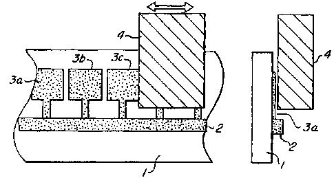
Figure 4 is a view of a second embodiment of the invention
wherein an inductive coupling is realised. On a carrier 1,
which may also be provided with an electrically conductive
layer on the rear side, a conductor structure 2 is provided,
too, which connects inductive coupler elements 3a to 3c. The
coupler elements 3a to 3c are configured here in the manner of
a conductor loop. The reference numeral 4 denotes again a cou-
pler means of the conventional type.
The inventive device of which an exemplary description has been
given above with reference to Figs. 1 to 4 presents a number of
advantages as will be explained in more details below, with
reference being made to Figs. 5 to 7.
Fig. 5 shows an embodiment wherein the inventive device is so
configured that it may be mounted on a rotary transformer, for
instance. The conductor structure 2 having the inventive design
with capacitive elements 3 (and/or inductive elements) may be
made of a plane film or foil or the printed circuit board 1 in
which slots are produced so as to allow for bending to small
radii. This were impossible with a strip line as it is common
in prior art.
Moreover, the inventive device presents the advantage that with
a bent arrangement and with a differential signal coupling only
slightly different line lengths are obtained which lead to dif-
CA 02276338 1999-06-29
22 PCTIDE 98100512
ferences in delay times and hence in signal noise and undesir-
able radiation. The inventive device is thus particularly well
suitable for the transmission of differential signals, which
entails the further advantage that the radiation to the outside
is minimised due to the fields in the outside space which com-
pensate each other practically almost completely.
Fig. 6 shows a comparison between conventional strip lines SL
designed as differential structure (figure section a) and an
inventive device (figure section b).
As becomes apparent from Figures 6a and 6b the lines 2 and 12
with coupler elements 3 and 13 are disposed very close to each
other in the case of an inventive device so that the difference
of their radii rl and rZis very small and hence the difference
in delay times becomes comparatively great.
Fig. 7a shows a simplified electrical equivalent circuit dia-
gram of an inventive device. As is shown in Fig. 7a, the inven-
tive device presents a low-pass characteristic. Thus the inven-
tive device entails the advantage of a high resistance to noise
because any noise above the threshold frequency will not be
passed on and can hence neither be received nor emitted.
Fig. 7b is an exemplary illustration of the computed frequency
response of an inventive device, wherein the frequency is plot-
ted (in MHz) along the abscissa and the received signal (in V)
is plotted on the ordinate. As is apparent here the inventive
device presents a practically constant frequency response be-
tween 1 MHz and almost 300 MHz, which steeply drops to "zero"
at roughly 300 MHz in the illustrated embodiment. Threshold
frequencies other than 300 MHz - be they higher or lower - can,
of course, be implemented as well.
CA 02276338 1999-06-29
23 PCT/DE 98/00612
Fig. 8 is an illustration of an inventive arrangement with
resonance coupling, which consists of an inductive or capaci-
tive coupler element 83, respectively, which supplies a con-
sumer 84. This coupler element is supplemented with at least
one dummy element 82 to form a structure able to resonate. The
signalling means 85 generates a regenerative coupling signal
from resonance currents or voltages at the coupler element or
at the supplementing dummy elements, which signal has such an
amplitude and such a phase that the switching or amplifying
element 81, together with the dummy elements 82 and 83 joining
it, satisfies the condition of oscillation.
Fig. 9 is an exemplary illustration of an arrangement in corre-
spondence with the invention for the case of a capacitive
transmission means. The capacitive coupler element 93 supplies
the consumer 94. It is supplemented by the inductor 92 for
forming a structure capable of resonating. In this case the
signalling means consists of a current meter resistor 95 which
transmits a signal proportional to the series resonance current
to the switching or amplifying component 91 by inductance and
capacitance.
Fig. 10 shows an example of a particularly simple embodiment of
an inventive system in the case of parallel resonance on an in-
ductive coupler element. In this case the inductive coupler
element 103 supplies a consumer 104. The inductor is supple-
mented by the capacitor 102 so as to form a parallel resonance
circuit. This signalling means consists here of a voltage di-
vider with the two resistors 105 and 106, which taps a prede-
termined share of the parallel resonance voltage by inductance
and capacitance and passes them on to the switching or amplify-
ing component, respectively.
The present invention has so far been described by exemplary
embodiments without any restriction of the general inventive
CA 02276338 1999-06-29
24 PCT/DE 8M512
idea and general applicability. In particular, it is possible
to employ the invention not only for rotary transformers such
as in computer tomographs, radar towers etc. but also for
transformers adapted for linear movement such as those required
on cranes etc. Moreover, the invention may be used in trans-
formers performing a composite movement.