Note: Descriptions are shown in the official language in which they were submitted.
CA 02276510 2001-11-30
IMPROVED
THERMIONIC ELECTRIC CONVERTERS
Field of the Invention
The present invention relates generally to the field
of converting heat energy directly to electrical energy.
More particularly, an improved thermionic electric
converter is provided.
Background of the Invention
Heretofore, there have been known thermionic
converters such as those shown in U.S. Patent. Nos.
3,519,854, 3,328,611,4,303,845, 4,323,808, and 5,459,367,
which disclose various apparatus and methods for the
direct conversion of thermal energy to electrical energy.
In U.S. Pat. No.3,519,854, there is described a converter
using Hall effect techniques as the output current
collection means. The '854 patent teaches use of a stream
of electrons boiled off of an emissive cathode surface as
the source of electrons. The electrons are accelerated
toward an anode positioned beyond the Hall effect
transducer. The anode of the '854 patent is a simple
metallic plate, which has a heavily static charged member
circling the plate and insulated from it.
U.S. Pat. No. 3,328,611 discloses a spherically
configured thermionic converter, wherein a spherical
emissive cathode is supplied with heat, thereby emitting
electrons to a concentrically positioned, spherical anode
1
CA 02276510 1999-06-30
WO 98/32155 PCTIUS97/19983
under the influence of a control member and having a high
positive potential thereon and insulated from. As with
the '854 patent, the anode of the '511 patent is simply a
metallic surface.
U.S. Patent No. 4,303,845 discloses a thermionic
converter wherein the electron stream from the cathode
passes through an air core induction coil located within
a transverse magnetic field, thereby generating an EMF in
the induction coil by interaction of the electron stream
with the transverse magnetic field. The anode of the
'845 patent also comprises a metallic plate which has a
heavily static charged member circling the plate and
insulated from it.
U.S. Patent No. 4,323,808 discloses a laser-excited
thermionic converter that is very similar to the
thermionic converter,disclosed in the '845 patent. The
main difference is that the '808 patent discloses using a
laser which is applied to a grid on which electrons are
collected at the same time the potential to the grid is
removed, thereby creating electron boluses that are
accelerated toward the anode through an air core
induction coil located within a transverse magnetic
field. The anode of the '808 patent is the same as that
disclosed in the '845 patent, i.e., simply a metallic
plate which has a heavily static charged member circling
the plate and insulated from it.
U.S. Patent 5,459,367 advantageously uses an
improved collector element with an anode having copper
2
CA 02276510 1999-06-30
WO 98/32155 PCT/US97/19983
wool fibers and copper sulfate gel instead of a metallic
plate. Additionally; the collector element has a highly
charged (i.e., static electricity) member surrounding the
anode and insulated from it.
Another prior design has an anode and cathode which
are relatively close together such as two microns apart
within a vacuum chamber. Such a prior design uses no
attractive force to attract electrons emitted from the
cathode to the anode other than induction of cesium into
the chamber housing the anode and cathode. The cesium
coats the anode with a positive charge to keep the
electrons flowing. With the cathode and anode so close
together, it is difficult to maintain the temperatures of
the cathode and anode at substantially different
temperatures. For example, one would normally have the
cathode at 1800 degrees Kelvin and the anode at 800
degrees Kelvin. A heat source is provided to heat the
cathode and a coolant circulation system is provided at
the anode in order to maintain it at the desired
temperature. Even though the chamber is maintained at a
vacuum (other than the cesium source), heat from the
cathode goes to the anode and it takes a significant
amount of energy to maintain the high temperature
differential between the closely spaced cathode and
' 25 anode. This in turn lowers the efficiency of the system
substantially.
3
CA 02276510 1999-06-30
WO 98/32155 PCT/US97/19983
OBJECTS AND SUMMARY OF THE INVENTION
Accordingly, an object of the present is to provide
and new and improved thermionic electric converter.
A more specific object of the present invention is
provide a thermionic electric converter with improved
conversion efficiency.
Yet another object of the present invention is to
provide an improved cathode for a thermionic electric
converter.
A further object of the present invention is to
provide a thermionic electric converter having the
cathode and anode spaced apart significantly such that
they are relatively thermally isolated from each other.
Yet another object of the present invention is to
provide a thermionic electric converter wherein energy
can be removed from electrons just before they strike the
anode.
The above and other objects of the present
invention, which will be apparent as the description
proceeds, are realized by a thermionic electric converter
having a casing member, a cathode within the casing
member operable when heated to serve as a source of
electrons, and an anode within the casing member operable
to receive electrons emitted from the cathode. The
cathode is a wire grid having wires going in at least two
directions that are transverse to each other. A charged
first focusing ring is in the casing member, between the
4
CA 02276510 1999-06-30
WO 98132155 PCTIUS97/19983
cathode and the anode, and is operable to direct
electrons emitted by-the cathode through the first
focusing ring on their way to the anode. A charged
second focusing ring is in the casing member, between the
first focusing ring and the anode, and is operable to
direct electrons emitted by the cathode through the
second focusing ring on their way to the anode.
Additional focusing rings may be necessary. The cathode
is preferably separated from the anode by 4 microns to
l0 five centimeters. More preferably, the cathode is
separated from the anode by one to three centimeters. A
laser operable to hit electrons (i.e., apply a laser beam
to the electrons) between the cathode and anode. The
laser hits the electrons just before they reach the
anode. The laser is operable to provide quantum
interference with the electrons such that electrons are
more readily captured by the anode.
The wire grid of the cathode preferably includes at
least four layers of wires. Further, each of the wire
layers has wires extending in a different direction from
each of the other of the wire layers, the wire grid of
the cathode thus including wires extending in at least
four different directions. This is designed to greatly
increase the emissive surface of the cathode.
' 25 The present invention may alternately be described
as a thermionic electric converter having a casing
member, a cathode within the casing member operable when
heated to serve as a source of electrons, an anode within
5
CA 02276510 1999-06-30
WO 98132155 PCTlUS97/19983
the casing member operable to receive electrons emitted
from the cathode; and a laser operable to hit electrons
between the cathode and anode. The laser thus provides
quantum interference with the electrons such that
electrons are more readily captured by the anode. The
laser is operable to hit electrons just before they reach
the anode. The laser is operable to hit electrons within
2 microns of when they reach the anode. The cathode is a
wire grid having wires going in at least two directions
l0 that are transverse to each other. The cathode is
separated from the anode by 4 microns to five
centimeters.
The present invention may alternately be described
as a thermionic electric converter having a casing
member, a cathode within the casing member operable when
heated to serve as a source of electrons, and an anode
within the casing member operable to receive electrons
emitted from the cathode and which proceed generally
along a movement direction defining the direction from
the cathode to the anode. The cathode has a planar cross
section area normal to the movement direction, the
cathode has an electron emission surface area for
electron emission towards the anode, and the electron
emission surface area is at least 30 percent greater than
the planar cross section area. The cathode is a wire
grid having wires going in at least two directions that
are transverse to each other. Alternately, or
additionally, the cathode is curved in at least one
6
CA 02276510 1999-06-30
WO 98!32155 PCT/US97119983
direction perpendicular to the movement direction. A
laser operable to hit electrons between the cathode and
anode just before they reach the anode. Preferably, the
electron emission surface area is at least double the
planar cross section area. More preferably, the electron
emission surface area is at least double the planar cross
section area. The smaller the diameter of the wire the
larger the emissive area. This is an exponential
relationship.
BRIEF DESCRIPTION OF THE DRAWINGS
The invention will be described in detail herein
with reference to the following figures in which like
reference numerals denote like elements, and wherein:
FIG. 1 is a schematic diagram of a prior art
thermionic electric converter;
FIG. 2 is a schematic diagram of a prior art laser-
excited thermionic electric converter;
FIG. 3 is a side view with parts in cross section
and schematic diagram of a thermionic electric converter
according to the present invention;
FIG. 4 is a top view of a wire grid structure used
for a cathode;
FIG. 5 is a side view of a part of the wire grid
structure;
FIG. 6 is a side view of a part of an alternate wire
grid structure;
7
CA 02276510 2002-O1-31
FIG. '7 is a side schematic diagram multiple layers
in a wire grid structure; and
FIG. 8 is a simplified side view of an alternate
cathode structure.
DETAILED DESCRIPTION of THE HREFERRED EMBODIMENT
FIGS. 1 and 2 show prier art thertnionie electric
converters as shown and described in U.S. Patent Nos.
4.303,845 and 4,323,808, respectively, both to Edwin D.
~o Davis, the inventor of the pr~sent invention. While the
operation of both thermionie converters i.s described in
detail in the above patents, a general operational
ovex-view is presented herein with, reference to FIGS. 1
and 2. This may provide background useful. in
i5 understanding the present invention.
FIG. 1 shows a basic thermionic e~.eetrie converter.
FIG. 2 shows a laser-excited thexmionie cor~.verter. The
operation of both converters is very similar.
with reference to the FIGS., a basic thex~mionic
2o electric converter ~.4 is shown. The eonvexter 1.0 has an
elongated, cylindrically shaped outer housing 12 fitted
with a pair of end walls 14 and i6, thereby form~.ng a
closed chamber 18. The housing 12 is made of any of a
number of kxaown strong, electrically non-conductive
25 materials, such as, for example, high-temperature
plastics or ceramics, while the end walls 14, 16 are
metallic plates to Which electrical connections may be
a
CA 02276510 1999-06-30
WO 98/32155 PCT/US97/19983
made. The elements are mechanically bonded together and
hermetically sealed such that the chamber 18 may support
a vacuum, and a moderately high electrical potential may
be applied and maintained across the end wails 14 and 16.
The first end wall 14 contains a shaped cathode
region 20 having an electron emissive coating (not shown)
disposed on its interior surface, while the second end
wall 16 is formed as a circular, slightly convex surface
which is first mounted in an insulating ring 21 to form
an assembly, all of which is then mated to the housing
12. In use, the end walls 14 and 16 function
respectively as the cathode terminal and the collecting
plate of the converter 10. Between these two walls, an
electron stream 22 will flow substantially along the axis
of symmetry of the cylindrical chamber 18, originating at
the cathode region 20 and terminating at the collecting
plate 16.
An annular focusing element 24 is concentrically
positioned within the chamber 18 at a location adjacent
to the cathode 20. A baffle element 26 is concentrically
positioned within the chamber 18 at a location adjacent
to the collecting plate 16.
Disposed between these two elements is an induction
assembly 28 comprised of a helical induction coil 30 and
' 25 an elongated annular magnet 32. The coil 30 and the
magnet 32 are concentrically disposed within, and occupy
the central region of, the chamber 18. Referring briefly
to the schematic end view of FIG. 2, the relative radial
9
CA 02276510 1999-06-30
WO 98132155 PCTIUS97/19983
positioning of the various elements and assemblies may be
seen. For clarity of-presentation, the mechanical
retaining means for these interiorly located elements
have not been included in either figure. Focusing
element 24 is electrically connected by means of a lead
34 and a hermetically sealed feed through 36 to an
external source of static potential (not shown). The
induction coil 30 is similarly connected via a pair of
leads 38 and 40 and a pair of feed-throughs 42 and 44 to
an external load element shown simply as a resistor 46.
The potentials applied to the various elements are
not explicitly shown nor discussed in detail as they
constitute well known and conventional means for
implementing related electron stream devices. Briefly,
considering (conventionally) the cathode region 20 as a
voltage reference level, a high, positive static charge
is applied to the collecting plate 16 and the external
circuit containing this voltage source is completed by
connection of its negative side to the cathode 20. This
applied high, positive static charge causes the electron
stream 22 which originated at the cathode region 20 to be
accelerated towards the collecting plate 16 with a
magnitude directly dependent upon the magnitude of the
high static charge applied. The electrons impinge upon
the collecting plate 16 at a velocity sufficient to cause
a certain amount of ricochet. The baffle element 26 is
configured and positioned to prevent these ricochet
electrons from reaching the main section of the
CA 02276510 1999-06-30
WO 98/32155 PCT/US97/19983
converter, and electrical connections (not shown) are
applied thereto as required. A negative voltage of low
to moderate level is applied to the focusing element 24
for focusing the electron stream 22 into a narrow beam.
In operation, a heat source 48 (which could be derived
from diverse sources such as combustion of fossil fuels,
solar devices, atomic devices, atomic waste or heat
exchangers from existing atomic operations) is used to
heat the electron emissive coating on the cathode 20,
thereby boiling off quantities of electrons. The
released electrons are focused into a narrow beam by
focusing element 24 and are accelerated towards the
collecting plate 16. While transiting the induction
assembly 28, the electrons come under the influence of
the magnetic field produced by the magnet 32 and execute
an interactive motion which causes an EMF to be induced
in the turns of the induction coil 30. Actually, this
induced EMF is the sum of a large number of individual
electrons executing small circular current loops thereby
developing a correspondingly large number of minute EMFs
in each winding of the coil 30. Taken as a whole, the
output voltage of the converter is proportional to the
velocity of the electrons in transit, and the output
current is dependent on the size and temperature of the
electron source. The mechanism for the induced EMF may
be explained in terms of the Lorentz force acting on an
electron having an initial linear velocity as it enters a
substantially uniform magnetic field orthogonally
11
CA 02276510 1999-06-30
WO 98/32155 PCT/US97/19983
disposed to the electron velocity. In a properly
configured device, a-spiral electron path (not shown)
results, which produces the desired net rate of change of
flux as required by Faraday's law to produce an induced
EMF.
This spiral electron path results from a combination
of the linear translational path (longitudinal) due to
the acceleration action of collecting plate 16 and a
circular path (transverse) due to the interaction of the
initial electron velocity and the transverse magnetic
field of magnet 32. Depending on the relative magnitude
of the high voltage applied to the collecting plate 16
and the strength and orientation of the magnetic field
produced by the magnet 32, other mechanisms for producing
a voltage directly in the induction coil 30 may be
possible. The mechanism outlined above is suggested as
an illustrative one only, and is not considered as the
only operating mode available. All mechanisms, however,
would result from various combinations of the applicable
Lorentz and Faraday considerations.
The basic difference between the basic converter
shown in U.S. Patent No. 4,303,845 and the laser-excited
converter shown in U.S. Patent No. 4,323,808, is that the
laser-excited converter collects electrons boiled off the
surface of the cathode on a grid 176 having a small
negative potential applied thereon by a negative
potential source 178 through lead 180, which traps the
electron flow and mass of electrons. The electrical
12
CA 02276510 1999-06-30
WO 98/32155 PCT/US97119983
potential imposed on the grid is removed, while the grid
is simultaneously exposed to a laser pulse discharge from
laser assembly 170, 173, 174, 20 causing a bolus of
electrons 22 to be released. The electron bolus 22 is
then electrically focused and directed through the
interior of the air core induction coils located within a
transverse magnetic field, thereby generating an EMF in
the induction coil which is applied to an external
circuit to perform work, as set forth above with respect
to to the basic thermionic converter.
As set forth the present inventor's prior U.S.
Patent 5,459,367, there are numerous attendant
disadvantages usually associated with having a collecting
element simply made up of a conductive metal plate.
Therefore, the collecting element of that design includes
a conductive layer of copper sulfate gel impregnated with
copper wool fibers. The present invention may use such
an anode. However, the present invention also may use a
conductive metal plate anode as other aspects of the
present invention will minimize or avoid some of the
disadvantages that such a plate anode might otherwise
cause. Basically then, the specifics of the anode are
not central to the preferred design of the present
invention.
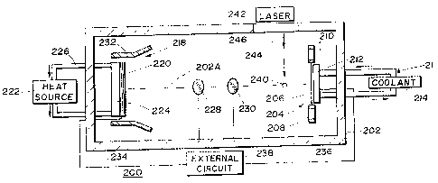
With reference now to FIG. 3, a thermionic electric
converter 200 according to the present invention includes
a casing member 202 in which a vacuum would be maintained
by vacuum apparatus (not shown) in known fashion. The
13
CA 02276510 1999-06-30
WO 98132155 PCT/US97/19983
casing member 202 is preferably cylindrical about a
central axis 202A which serves as an axis of symmetry of
the member 202 and the components therein except where
otherwise noted.
The collector 204 may include a flat anode circular
plate 206 (made of copper for example) surrounded by a
statically charged ring 208 (charged to 1000 Coulombs for
example) having insulating rings 210 concentric
therewith. The ring 208 and rings 210 may be constructed
and operable as discussed in the 5,459,367 Patent. A
cooling member 212 is thermally coupled to the plate 206
such that coolant from coolant source 214 is recirculated
therethrough by coolant circuit 216. The cooling member
212 maintains the anode plate at a desired temperature.
The cooling member 212 may alternately be the same as the
anode plate 206 (in other words coolant would circulate
through plate 206). A feedback arrangement (not shown)
using one or more sensors (not shown) could be used to
stabilize the temperature of anode 206.
The catrode assembly 218 of the present invention
includes a cathode 220 heated by a heat source such that
it emits electrons which generally move along movement
direction 202A towards the anode 206. (As in the
5,459,367 Patent, the charged ring 208 helps attract the
electrons towards the anode.) Although the heat source
is shown as a source 222 of heating fluid {liquid or gas)
flowing to heating member 224 (which is thermally coupled
to the cathode 220) via heating circuit 226, alternate
14
CA 02276510 2001-11-30
energy sources such as a laser applied to the cathode 220
might be used. The energy input into source 222 could be
solar, laser, microwave, or radioactive materials.
Further, used nuclear fuel that would otherwise simply be
stored at great expense and without benefit might be used
to provide the heat to source 222.
Electrons energized to the Fermi level in cathode
220 escape from the surface thereof and, attracted by
static charge ring 208, travel along movement direction
202A through first and second focussing rings or
cylinders 228 and 230, which may be constructed and
operable in similar fashion focussing element 24 of the
prior art arrangement discussed above. In order to help
the electrons move in the proper direction a shield 232
may surround the cathode 220. The shield 232 may be
cylindrical or conical or, as shown, include a
cylindrical portion closest the cathode 220 and a conical
portion further from the cathode 220. In any case, the
shield tends to keep electron movement in direction 202A.
The electrons will tend to be repelled from the shield
232 since the shield will be at a relatively high
temperature (from its proximity to the relatively high
temperature cathode 220). Alternately, or additionally,
to being repelled by the high temperature of the shield,
the shield 232 could have a negative charge applied to
it. In the later case, insulation (not shown) could be
used between the shield 232 and cathode 220.
CA 02276510 1999-06-30
WO 98/32155 PCT/US97119983
The electrical energy produced corresponding to
electron flow from cathode 220 to anode 206 is supplied
via cathode wire 234 and anode wire 236 to an external
circuit 238.
Turning from the overall operation of the converter
200 to specific advantageous aspects thereof, electrons
such as electron 240 tend to have a high energy level as
they approach the anode 206. Therefore, the normal
tendency would be for some to bounce off the surface and
not be captured therein. This normally results in
electron scatter and diminishes the conversion efficiency
of a converter. In order to avoid or greatly reduce this
tendency, the present invention uses a laser 242 which
hits the electrons (e. g., hits them with a laser beam
244) just before they hit the anode 206. The quantum
interference between the photons of the laser beam 244
and the electrons 240 drops the energy state of the
electrons such that they are more readily captured by the
surface of anode 206.
As will be understood from the dual wave-particle
theory of physics, the electrons hit by the laser beam
may be exhibiting properties of waves and/or particles.
(Of course, the scope of the claims on the present
invention are not limited to any particular theory of
operation unless and except where a claim expressly
references such a theory of operation, such as quantum
interference.)
16
CA 02276510 1999-06-30
WO 98/32155 PCT/US97/19983
As used herein, saying that the laser 242 hits the
electrons with beam 244 "just before" the electrons reach
the anode 206 means that the electrons which have been
hit do not pass through any other components (such as a
focussing member) as they continue to the anode 206.
More specifically, the electrons are preferably hit
within 2 microns of when they reach the anode 206. Even
more preferably, the electrons are hit by the laser with
1 microns of reaching the anode 206. Indeed, the
distance from the second focussing element 230 to the
anode 206 may be 1 micron and the laser may hit electrons
closer to the anode 206. In that fashion (i.e., hitting
the electrons just before they reach the anode), the
energy of the electrons is reduced at a point where
reduced energy is most appropriate and useful.
Although casing member 202 may be opaque, such as a
metal member, a laser window 246 is made of transparent
material such that the laser beam 244 can travel from
laser 242 into the chamber within member 202.
Alternately, the laser 242 could be disposed in the
chamber.
In addition to improving conversion efficiency by
using the laser 242 to reduce the energy level of
electrons just before they reach the anode 206, the
- 25 cathode 220 of the present invention is specifically
designed to improve efficiency by increasing the electron
emission area of the cathode 220.
17
CA 02276510 1999-06-30
WO 98/32155 PCTlUS97/19983
With reference to FIG. 4, the cathode 220 is shown
as a circular grid of-wires 248. Wires 250 of a top or
first layer of parallel wires extend in direction 252,
whereas wires 254 of a second layer of parallel wires
extend in direction 256, transverse to direction 252 and
preferably perpendicular to direction 252. A third layer
of parallel wires (only one wire 258 shown for ease of
illustration) extend in direction 260 (45 degrees from
directions 252 and 256. A fourth layer of parallel wires
(only one wire 262 shown for ease of illustration) extend
in direction 264 (90 degrees from direction 260).
It should also be noted that FIG. 4 shows the wires
with relatively large separation distances between them
but this is also for ease of illustration. Preferably,
the wires are finely extruded wires and the separation
distances between parallel wires in the same layer would
be similar to the diameter of the wires. Preferably, the
wires have diameters of 2 mm or less to fine filament
size. The wires may be tungsten or other metals used in
cathodes.
With reference to FIG. 5, the wires 250 and 254 may
be offset from each other with all wires 250 (only one
shown in FIG. 5) disposed in a common plane offset from a
different common plane in which all wires 254 are
disposed. An alternate arrangement shown in FIG. 6 has
wires 250' (only one visible) and 254' which are
interwoven in the manner of fabric.
18
CA 02276510 1999-06-30
WO 98/32155 PCTIUS97119983
With reference to FIG. 7, an alternate cathode 220'
may have three portions 266, 268, and 270. Each of
portions 266, 268, and 270 may have two perpendicular
layers of wires (not shown in FIG. 7) such as 250 and 254
(or 250' and 254'). Portion 266 would have wires going
into the plane of view of FIG. 7 and wires parallel to
the plane of FIG. 7. Portion 268 has two layers of
wires, each having wires extending in a direction 30
degrees from one of the directions of the wires for
portion 266. Portion 270 has two layers of wires, each
layer having wires extending in a direction 60 degrees
from one of the directions of the wires for portion 266.
It will be appreciated that FIG. 7 is illustrative
of the point that multiple layers of wires extending in
different directions could be used.
The various wire grid structures for the cathode
increase the effective electron emission surface area by
way of the shape of the wires and their multiple layers.
An alternative way of increasing the surface area is
illustrated in FIG. 8. FIG. 8 shows a side cross section
view of a parabolic cathode 280 operable to emit
electrons for movement generally along movement direction
220A'. The cathode 280 has a planar cross section area A
normal to the movement direction 202A. Significantly,
the cathode 280 has an electron emission surface area EA
(from the curvature of the cathode) for electron emission
towards the anode which is at least 30 percent greater
than the planar cross section area A. Thus, a greater
19
CA 02276510 1999-06-30
WO 98/32155 PCTlLTS97/19983
density of electrons are generated for a given size
cathode. Although the cathode 280 is shown as a
parabola, other curved surfaces may be used. The cathode
280 may be made of a solid member or may also incorporate
multiple layer wire grid structures like described for
FIGS. 4-7 except that each layer would be curved and not
planar.
Although the curved cathode arrangement of FIG. 8
provides an electron emission surface area EA that is at
least 30 percent greater than the side cross section area
A, the various wire grid arrangements such as FIG. 4
provide an electron emission surface area that is at
least double the side cross section area (i.e., defined
as shown for FIG. 8). Indeed, the electron emission
surface area in the grid arrangements should be at least
ten times the side cross section area.
Advantageously, the present invention allows the
cathode 220 and anode 206 to be offset from each other by
from 4 microns to 5 cm. More specifically, that offset
or separation distance will be from 1 to 3 cm. Thus, the
cathode and anode are sufficiently far apart that heat
from the cathode is less likely to be conveyed to the
anode than in the arrangements where the cathode and
anode must be in close proximity. Therefore, the coolant
source 214 can be a relatively low coolant demand
arrangement since less cooling is required than in many
prior designs.
CA 02276510 1999-06-30
WO 98/32155 PCTIUS97/19983
While the invention has been described in
conjunction with specific embodiments thereof, it is
evident that many alternatives, modifications and
variations will be apparent to those skilled in the art.
Accordingly, the preferred embodiments of the invention,
as set forth herein, are intended to be illustrative, not
limiting. Various changes may be made without departing
from the spirit and scope of the invention as defined
herein and in the following claims.
21
fi.