Note: Descriptions are shown in the official language in which they were submitted.
CA 02276834 1999-07-OS
. v
- 1 -
DIRECTIONAL COUPLER, ANTENNA DEVICE, AND TRANSCEIVER
BACKGROUND OF THE INVENTION
1. Field of the Invention
The present invention relates to a directional coupler
using a dielectric guide, and to an antenna device and a
transceiver using the directional coupler.
2. Description of the Related Art
Conventionally, a dielectric guide, comprising a
dielectric strip provided between two conductive plates, is used
as a guide for transmission in the milliwave band and the like.
When forming a milliwave circuit using such dielectric guides,
a directional coupler is used in a portion where electrical power
is split between two dielectric guides.
A conventional directional coupler using dielectric
guides comprises two dielectric strips, having a linear portion
and a curved portion, which are provided at a predetermined
distance apart between two conductive plates. The dielectric
strips are arranged close together and the dielectric guides are
coupled at this closely arranged portion.
A milliwave radar is an example of the milliwave circuit
using dielectric guides described above. An antenna device used
in a milliwave radar comprises a dielectric lens and a primary
emitter provided at the focal point of the dielectric lens.
However, since the direction of the antenna in the
CA 02276834 1999-07-OS
- 2 -
conventional milliwave radar is fixed, in certain conditions it
is not possible to achieve the intended sensitivity and
measurements, as will be explained below. For instance, as shown
in FIG. 22, when a vehicle is traveling on a multi-lane road,
it is not possible to determine immediately whether other
vehicles in front of it are traveling in the same lane based only
on waves reflected from the other vehicles. That is, in FIG.
22, when the vehicle Cm emits a beam B2, it picks up not only
waves reflected from the vehicle Ca which is traveling in front,
but also waves reflected from the vehicle Cb which is traveling
in the opposite lane. Furthermore, as shown in the example of
FIG. 23, when the vehicle Cm emits a beam B1 in the forward
direction, it is unable to detect the vehicle Ca which is
traveling in front in the same lane. Moreover, as shown in FIG.
24, when traveling on an curving road, even though the vehicle
Cm emits a beam B1 in the forward direction, it cannot detect
the vehicle Ca in front of it.
One conceivable solution is to provide an antenna device,
combining a primary emitter and a dielectric lens, in which the
direction of the beam is tilted by changing the position of the
primary emitter. In order to change the position of the primary
emitter, the configuration should be arranged so that the
dielectric guide connecting to the primary emitter and the other
dielectric guide connecting to the circuit can be relatively
displaced while remaining coupled with low loss . To achieve this,
CA 02276834 1999-07-OS
- 3 -
the configuration of the directional coupler using dielectric
guides described above need only be arranged so that two
dielectric guides can be relatively displaced.
However, the separated positions (separated faces) of
the two dielectric guides of the directional coupler are
parallel to the two dielectric strips provided closely together.
With this configuration, the end faces of the conductive plates
on either side of the dielectric strips are provided parallel
to the direction of propagation of the electromagnetic waves of
the two dielectric guides, and consequently the path of the
current flowing through the conductive plates is broken at the
end face portions of the conductive plates, causing reflection.
As a result, there are problems such as the creation of unwanted
modes other than the propagation mode, increased loss, or an
inability to obtain desired characteristics of the directional
coupler, etc.
The above example describes case where the two dielectric
guides of the directional coupler portion are relatively
displaced, but the directional coupler can be used when forming
a single device incorporating circuit modules using dielectric
guides, to couple the dielectric guides between the circuit
modules. In this case too, the path of the current flowing
through the conductive plates is broken between the circuit
modules, causing reflection. As a result, there are problems
of increased loss and inability to obtain desired signal
CA 02276834 1999-07-OS
- 4 -
transmission characteristics between the circuit modules.
SOMMARY OF THE INVENTION
Accordingly, it is an object of the present invention to
provide a directional coupler comprising two separated
dielectric guides, wherein the above problems of reflection and
loss are eliminated.
To provide dielectric strips of two dielectric guides of
a directional coupler close together in a predetermined region
only, a bend must be provided in dielectric guide portions joined
to the directional coupler. However, to reduce loss due to
conversion from the LSM mode to the LSE mode, for instance, the
radius of curvature of the bend must be large. As a result, the
overall size of the device is increased, and when it is used to
form an antenna device, the moving portion cannot be made light,
making it difficult to deflect the beam quickly. On the other
hand, when the space between opposing faces of the two conductive
plates clasping the dielectric strip is made narrow, although
the radius of curvature of the bend can be set freely as long
as dielectric guides transmitting only in the LSMO1 mode as used,
the coupling portion must be made long in order to obtain
adequate coupling, inevitably increasing the overall size of the
device and making it difficult to lighten the moving portion.
If the space between the dielectric strips in the coupling
portion is extremely narrow, strong coupling can be obtained,
CA 02276834 2001-10-17
but the characteristics of the directional coupler will
greatly depend on the precision of the positioning of the
two separated dielectric guides.
It is another object of the present invention
enable the directional coupler and a device using the
directional coupler to be easily miniturized, to enable
the mass of the moving portion to be reduced, and to
enable the direction of the beam to be deflected quickly.
According to an aspect of the present invention,
there is provided a directional coupler comprising:
first and second dielectric guides, each
comprising a dielectric strip provided between two
conductive plates and using opposing faces of said t:wo
conductive plates as electrode faces, the conductive
plates having end faces substantially perpendicular to
the opposing faces,
said first and second dielectric guides being
arranged with end,faces of their respective conductive
plates adjacently, t:he dielectric strips of said first
and second dielectric guides being provided substantially
parallel to each other in the vicinity of the end faces
of said conductive plates, and a groove being provided in
an end face of said conductive :plates of one of said.
first and second dielectric guides, the groove having a
short-circuiting face in a position at a distance from
said electrode faces of approximately an integral
multiple of half the wavelength of a propagated wave.
With this configuration, the electrode faces in
the portion where the end faces of the conductive plates
of the first and second dielectric guides are aligned
function as an
CA 02276834 1999-07-OS
- 6 -
equivalently continuous portion. Therefore, although the two
dielectric guides are separated by the conductive plate portions,
there is almost no loss in this space. Furthermore, since there
is almost no reflection, no spurious modes are caused by
reflection.
Furthermore, in the present invention, a position at a
distance from the electrode face of approximately an integral
multiple of half the wavelength of a plane wave, which travels
in a direction such that it has a wave-number vector component
equal to a phase constant of a transmitted wave propagating
through the dielectric guides, in the direction of a transmitted
wave propagating through the dielectric guides, is a short-
circuiting face.
A plane wave, propagating through the aligned portion of
the end faces of the conductive plates of the first and second
diel8ctric guides, travels in a direction determined according
to its size and the size of a transmission wave, propagating
along the length of the dielectric guides. That is, the size
of the plane wave ( wave-number k ) is predetermined, and when the
plane wave is projected in the transmission direction of the
dielectric guides, the plane wave proceeds in a direction (8)
which matches the phase constant of a transmission wave
propagating through the dielectric guides. Therefore, when a
groove is provided as a short-circuiting face at a distance from
the electrode face of approximately an integral multiple of half
CA 02276834 1999-07-OS
the wavelength of a plane wave in that direction, the problem
of reflection is avoided to an optimum degree.
Furthermore, the present invention further comprises a
first type of nonradiative dielectric guide comprising the
approximately parallel dielectric strip portions and the
electrode faces, and a second type of nonradiative dielectric
guide, wherein the space between the electrode faces other than
those of the approximately parallel dielectric strip portions
is narrower than the height of the approximately parallel
dielectric strip portions, and comprising a dielectric strip
portion other than the approximately parallel dielectric strip
portions and the electrode faces, and transmitting in a single
LSMO1 mode. Then, a guide conversion portion is provided between
the first and second types of nonradiative dielectric guide.
Consequently, coupling can easily be achieved in the first type
of nonradiative dielectric guide portion, without increasing
the length of the parallel dielectric strip portions or greatly
narrowing the space between them. In addition, in the second
type of nonradiative dielectric guide portion, there is no
conversion to the LSE mode even when a bend with a short radius
of curvature is provided, thereby enabling the entire device to
be miniturized without increasing transmission loss.
Furthermore, according to the present invention, a
primary emitter is coupled to a first dielectric guide of the
above directional coupler, and a dielectric lens is secured
CA 02276834 2001-10-17
8
approximately at the focal point of the primary emitter.
With this configuration, when the first dielectric guide
is displaced in relation to a second dielectric guide,
the primary emitter is displaced within the focal point
inner face of the dielectric lens, tilting the direction
of the beam. Moreover, there is .little loss in the
directional coupler portion, and the moving portion can
be miniturized and of low mass by providing the first and
second types of nonradiative dielectric guides on the
side of the first dielectric guide.
According to another aspect of the present
invention, there is provided an antenna device comprising
the directional coupler according to one of the above
aspects of the present invention, a primary emitter
coupled to a first dielectric guide of said directional
coupler, and a dielectric lens provided approximately at
the focal point of said primary emitter and secured to a
second dielectric guide of said directional coupler.
When the directional coupler is arranged so that the
amount of coupling between the first dielectric guide and
the second dielectric guide of the directional coupler is
approximately 0 dB, transmission signals and received
signals can be transmitted most efficiently between the
moving portion and the fixed portion, increasing the
efficiency of the antenna.
Furthermore, in the present invention, a
transmission signal is sent from a transmitter to the
second dielectric guide, and input/output ports of a
circulator for sending a received signal from the second
dielectric guide to a receiver are connected to the
second dielectric guide. With this configuration, it is
possible to realize an antenna device for transmitting
and receiving, in which the direction of the beam can be
tilted using a single primary emitter and a single
CA 02276834 2001-10-17
directional coupler.
Furthermore, the present invention comprises a
transceiver wherein a transmitter is connected to an
input port of the c:Lrculator in the antenna device, and a
receiver is connected to an output port of the circulator
in the antenna device.
BRIEF DESCRIPTION OF THE DRAWINGS
FIGS. 1A and 1B show configurations of a
directional coupler and an antenna device according to a
first embodiment;
FIGS. 2A to 2C are diagrams showing the relation
between relative positions of a dielectric lens and a
primary emitter and the direction of a beam;
FIG. 3 is a cross-sectional view of a directional
coupler portion;
FIGS. 4A and 4B are partial cross-sectional views
of the configuration of end faces of conductive plates of
a directional coup:Lex~;
FIGS. 5A to 5E are cross-sectional views of
various example configurations of a directional coupler;
FIGS. 6A and 6B are diagrams showing the relation
between the configuration of a directional coupler and
its characteristics;
FIGS. 7A and 7B are diagrams showing a cross-
sectional configuration of two types of directional
coupler;
FIG. 8 is a perspective view of a configuration of
a guide
CA 02276834 1999-07-OS
- 10 -
converter portion;
FIGS . 9A and 9B are a top view and a cross-sectional view,
respectively, of the configuration of the same guide converter
portion;
FIGS. 10A to lOD are diagrams showing example dimensions
of each part of a directional coupler;
FIGS . 11A to 11C are diagrams showing characteristics of
the same directional coupler;
FIGS. 12A to 12C are diagrams showing a configuration of
a directional coupler according to a second embodiment;
FIGS. 13A to 13C are diagrams showing an example
configuration of another directional coupler;
FIGS. 14A and 14B are diagrams showing a configuration
of another directional coupler having a differently configured
moving portion side;
FIG. 15 is a cross-sectional view of the configuration
of dielectric guides on a moving portion side;
FIG. 16 is a top view of an example configuration of
another directional coupler;
FIG. 17 is a diagram showing a configuration of a
transceiver;
FIG. 18 is an exploded perspective view of a
configuration of an antenna device and a transceiver;
FIG. 19 is a perspective view of an example configuration
of a forward-screw system;
CA 02276834 1999-07-OS
- 11 -
FIGS. 20A and 20B are diagrams showing an example
configuration of a voice-coil motor
FIG. 21 is a block diagram showing a configuration of a
milliwave radar for a vehicle;
FIG. 22 is a diagram showing the state when the emitted
beam of the milliwave radar for a vehicle is tilted horizontally;
FIG. 23 is a diagram showing the state when the emitted
beam of the milliwave radar for a vehicle is tilted horizontally;
FIG. 24 is a diagram showing the state when the emitted
beam of a milliwave radar for a vehicle is tilted vertically;
FIG. 25 is a partial perspective view of a configuration
of an aligned portion of two upper conductive plates;
FIG. 26 is a cross-sectional view of a configuration of
an aligned portion of the conductive plates;
FIG. 27 is a diagram defining ports of a directional
coupler;
FIG. 28 is a diagram showing measurements of transparency
characteristics of a directional coupler; and
FIGS. 29A and 29B are diagrams showing measurements of
transparency characteristics of a directional coupler as a
comparative example.
DESCRIPTION OF THE PREFERRED EMBODIMENTS
The configurations of a directional coupler and an
antenna device according to a first embodiment of the present
CA 02276834 1999-07-OS
- 12 -
invention will be explained with reference to FIGS. 1A to 11.
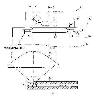
FIGS. 1A and 1B show the relation between the
configuration of a directional coupler and a primary emitter and
a dielectric lens . In FIG. 1A is a top view of the state when
the upper conductive plate is removed, and FIG. 1B is a
cross-sectional view through the primary emitter portion. In
FIG. 1A, a moving portion 31 can be displaced with respect to
a fixed portion 32 in the direction indicated by the arrows. In
the moving portion 31, numeral 14 represents a lower conductive
plate and numeral 11 represent a dielectric strip. The
dielectric strip 11 is provided between an upper conductive
plate and the lower conductive plate 14, thereby forming a first
nonradiative dielectric guide(hereinafter"NRD guide"). In the
fixed portion 32, numeral 16 represents a lower conductive plate
and 12 is a dielectric strip. The dielectric strip 12 is provided
between an upper conductive plate and the lower conductive plate
16, thereby forming a second NRD guide.
The end faces of the conductive plates of the first and
second NRD guides are provided with a predetermined gap in
between so that they do not contact each other . The dielectric
strips 11 and 12 of the first and second NRD guides are provided
close together in parallel near the end faces of the conductive
plates 14 and 16. Thus a directional coupler is formed,
comprising the first and second NRD guides.
Dielectric strip portions, shown in FIG. 1 by the
CA 02276834 1999-07-OS
- 13 -
portions 11' and 12' , and the upper and lower conductive plates
clasping them, form NRD guides ( hereinafter "hyper NRD guides" )
which transmit in a single mode, LSMO1 mode.
A primary emitter 13, comprising a cylindrical rod-like
dielectric resonator, is provided at an end of the dielectric
strip 11' of the moving portion 31. As shown in FIG. 1B, an
opening, having a horn-like taper, is provided in the upper
conductive plate 15 and is coaxial to the primary emitter 13.
As shown in the diagram, a slit plate, comprising a conductive
plate with a slit in it, is inserted between the primary emitter
13 and the opening. As a consequence, electromagnetic waves are
propagated in the dielectric strip 11 ' in an LSM mode carrying
electrical field components at a right angle to the length of
the dielectric strip 11' and parallel to the conductive plates
14 and 15, and carrying magnetic field components in a direction
perpendicular to the conductive plates 14 and 15. The dielectric
strip 11' and the primary emitter 13 are electromagnetically
coupled, generating an HE111 mode carrying electrical field
components inside the primary emitter 13 in the same direction
as the electrical field of the dielectric strip 11'. Then,
vertically polarized electromagnetic waves are emitted through
the opening in a direction perpendicular to the conductive plate
14. The dielectric lens 18 converges these waves into a
predetermined beam. Conversely, when electromagnetic waves are
emitted through a dielectric lens into the opening, the primary
CA 02276834 1999-07-OS
- 14 -
emitter 13 is excited in the HE111 mode, and electromagnetic
waves are propagated in the LSM mode to the dielectric strip 11'
coupled to it.
A terminator 20 is provided at one end of the dielectric
strip 12' on the fixed portion 32 side. With this configuration,
transmission signals are input to the hyper NRD guide comprising
the other dielectric strip 12', which outputs received signals.
FIG. 2 shows changes in direction of the beam due to
displacement of the primary emitter. The primary emitter 13 is
positioned approximately at the focal point of the dielectric
lens 18, and the transmitted/received beam B is deflected to the
left and right as shown in FIG. 2 by displacing the focal point
of the inner face (by displacing the moving portion 31 in
relation to the fixed portion 32 shown in FIG. 1A)
FIG. 3 is a cross-sectional view taken along the line A-A
of FIG. 1A. The first NRD guide on the moving portion side
comprises the upper and lower conductive plates 14 and 15, and
the dielectric strip 11 provided between them. The second NRD
guide on the moving portion side comprises the upper and lower
conductive plates 16 and 17, and the dielectric strip 12 provided
between them. The end faces of the conductive plates of the first
and second NRD guides are arranged opposite each other with a
predetermined gap between them, and predetermined grooves
running parallel to the conductive plates 16 and 17 are provided
in the end faces of the conductive plates 16 and 17.
CA 02276834 1999-07-OS
- 15 -
FIG. 4 shows two examples of the configuration of the
above grooves. In example FIG. 4A, a groove of depth d0 and
thickness g0 is provided at a distance of h0 from the electrode
face (the opposing faces of the upper and lower conductive
plates ) . Here, g0 is equal to the gap g between the conductive
plates 15 and 17. Further, h0 = d0, these lengths being an odd
multiple of a quarter of the wavelength of the electromagnetic
waves propagating through the gap. Since the end P3 of the groove
is a short-circuiting terminal, a point P2, which is a distance
d0 from the end P3, is an equivalently open point, and a point
P1, which is a distance h0 from the point P2, is an equivalently
short-circuiting point (short-circuiting face). Therefore, the
electrode faces of conductive plates 15 and 17 are equivalently
continuous.
As shown in the example of FIG. 4B, the width g1 of the
groove is wider than the gap g of the conductive plates 15 and
17. In such a configuration, the position, depth, and width of
the groove should be set so that the position of P1, as viewed
from the short-circuited face P3, is an equivalently short-
circuited face. Normally, the greater the width g1 of the groove,
the shorter the distance hl from the electrode face to the groove,
and consequently it is possible to make the point P2 portion
between the two conductive plates an equivalently open point.
When the portion between the two conductive plates is made an
open terminal in this manner, no current flows to the conductive
CA 02276834 1999-07-OS
- 16 -
plates, thereby reducing conductive loss.
Although the two NRD guides, comprising a moving portion
and a fixed portion, are separated at the conductive plate
portion, their electrode faces are equivalently continuous, and
so almost no loss is caused by the presence of the gap.
Furthermore, since there is almost no reflection in the space,
no spurious mode is caused by reflection.
FIGS. 5A to 5E show cross-sectional views of other
configurations of a coupling portion between two NRD guides. In
the example shown in FIG. 3, grooves were provided in the end
faces of both the upper and lower conductive plates; however,
as shown in FIG. 5A, grooves can be provided not only in the fixed
portion side but also in the moving portion side. Furthermore,
as shown in example FIG. 5B, grooves can be provided in opposite
parts of the upper and lower conductive plates of the fixed
portion and the moving portion. Alternatively , as in example
FIG. 5C, the grooves can be provided facing each other on both
sides. The thicknesses of the conductive plates of the fixed
portion and the moving portion do not necessarily have to be the
same, but when they differ, the opposing end faces of the
conductive plates should have the same thickness, as in FIG. 5D.
When the conductive plates 14 and 15 on the moving portion side
are made thin overall, the overall size and weight of the moving
portion can be made small, enabling it to be displaced easily
using even a low-torque motor. Furthermore, as shown in FIG.
CA 02276834 1999-07-OS
- 17 -
5E, a groove may be provided in just one of the conductive plates,
to achieve a desired effect.
In the example shown in FIG. 4, in a 60 GHz band, g = g0
- 0.2 mm, h0 = d0 = 1.2 mm. In FIG. 4H, g = 0.2 mm, g1 = 1.0
mm, hl = 0.96 mm and dl = 1.5 mm. In this example, the distance
from the end P3 of the groove to the electrode face P1 was half
the wavelength of the propagated waves, but this distance need
only be nT./2, where n is a whole number greater than 1, and ~,
is the wavelength. Furthermore, the distance from the electrode
face P1 and the groove end P3 to the midpoint P2 should be ( 2m
- 1 ) ~,/4 (where m is an integer greater than 1 ) . The longer the
distance from point P1 to point P3, the narrower the width of
the frequency band in which the point P1 can function
equivalently as a short-circuited face, and for this reason, the
distance from point P1 and point P3 to the midpoint P2 should
be approximately ~,/4 to obtain the above effect over a wide band.
FIG. 6 shows the relation between the directional coupler
described above and the power splitting ratio. Now, if the phase
constant of the even modes of the coupled guides, comprising the
dielectric strips 11 and 12, is expressed as Vie, the phase
constant of the odd modes as ~o, and ~~ _ ~ ~e - ~o~ , and the power
ratio between an electromagnetic wave input from port #1 and an
electromagnetic wave output to port #2 is expressed by P2/P1 =
1-sine (O~z/2 ) , and the power ratio between an electromagnetic
wave input from port #1 and an electromagnetic wave output to
CA 02276834 1999-07-OS
- 18 -
port #4 is expressed by P4/P1 = 1-sing (O~z/2 ) . Therefore, with
a constant of (~~z/2 ) = n~+x/2 ( n: 0, 1, 2 . . . ) , the entire input
from the port #1 is output to the port #4, forming an 0 dB
directional coupler.
FIGS . 7A and 7B show the cross-sectional configurations
of the hyper NRD guide and the normal NRD guide portion in the
directional coupler shown in FIG. 1. FIG. 7A is a cross-
sectional view of the NRD guide 12 taken along the line A-A of
FIG. 1, and FIG. 7B is a cross-sectional view taken along the
line B-B in FIG. 1. As shown in FIG. 7A, in the normal NRD guide,
the space Dh between the electrode faces of the conductive plates
16 and 17 is equal to the height of the dielectric strip 12. As
shown in FIG. 7B, in the hyper NRD guide, grooves of depth Gh
are provided in the conductive plates 16 and 17, so that the space
Eh between the electrode faces of the conductive plates 16 and
17 is narrower than the height Dh of the dielectric strip 12 ' .
In addition to providing these grooves, the space between the
propagation region of the dielectric strips and the conductive
break plate in the nonpropagation region where there are no
dielectric strips is determined, the dielectric constants of the
dielectric strips are determined, and the cut-off frequency of
the LSMO1 mode is set lower than the cut-off frequency of the
LSE01 mode, and the cut-off frequency of the LSE01 mode is set
higher than the frequency used. With this configuration, waves
can always be transmitted in a single mode, the LSMO1 mode,
CA 02276834 1999-07-OS
- 19 -
irrespective of the radius of curvature and the like of the bends
of the dielectric strips. Consequently, the overall directional
coupler can be made small with reduced loss.
When signals are transmitted at a single frequency, the
width DHw of the dielectric strip 12' of the hyper NRD guide is
smaller than the width DNw of the dielectric strip 12 of the
normal NRD guide. For instance, in a band of 60 GHz, if the
specific dielectric constant er of the dielectric strips is 2.04,
then Dh = 2.2 mm, DNw = 3.0 mm, Gh = 0.5 mm, Eh = 1.2 mm and DHw
- 1.8 mm.
FIG. 8 is a perspective view of the configuration of a
normal NRD guide, a hyper NRD guide, and a guide converter. FIG.
9 shows a top view and a cross-sectional view of the same. FIG.
8 and FIG. 9 show states when the upper conductive plate has been
removed. As shown in these diagrams, the converter portion of
the hyper NRD guide and the normal NRD guide is tapered so as
to gradually eliminate the dimensional difference in the widths
of the dielectric strips of the NRD guides. Furthermore, the
space between the electrode faces of the conductive plates 16
and 17 changes in stages. That is, the space between the
electrode faces of the hyper NRD guide does not change from the
position of the interface between the hyper NRD guide and the
converter to w1. Similarly, the space between the electrode
faces of the normal NRD guide does not change from the position
of the interface between the normal NRD guide and the converter
CA 02276834 1999-07-OS
- 20 -
to w2. However, in the portion between w1 and w2, the spaces
between the electrode faces of the normal NRD guide and the hyper
NRD guide have an intermediate value. For instance, w1 = w2 =
0.75 mm, w0 = 3.0 mm, ghl = 0.13 mm, gh2 = 0.37 mm. Here, w3
corresponds to approximately one-quarter of the wavelength of
the propagated waves. Consequently, a reflected wave 1 and a
reflected wave 2 are coupled in reverse phase in the step portion
of the space between the electrode faces, thereby cancelling the
emitted waves . As a result, the hyper NRD guide and the normal
NRD guide can be converted with no problem of reflection.
The above example described the configurations and
conversion portion of the hyper NRD guide and the normal NRD
guide on the fixed portion side, but the moving side is the same.
FIGS. 10A to lOD show sizes of all the portions when the
directional coupler described above is configured as an 0 dB
directional coupler, and FIG. 11 shows its characteristics.
FIGS. 10A to lOD show the dimensions of all the portions
in millimeters . FIG. 10A is a top view when the upper conductive
plate is removed, FIG. lOB is a cross-sectional view taken along
the line A-A of FIG. 10B, and FIG. lOC is a top view of the guide
converter portion of the normal NRD guide and the hyper NRD guide
and a cross-sectional view of the area near it. Finally, FIG.
lOD is a diagram showing the original position of the moving
portion.
FIG. 11 is a diagram showing transparency
CA 02276834 1999-07-OS
- 21 -
characteristics of the directional coupler when the moving
portion has been displaced by -8 mm, 0 mm and +8 mm to three
different positions, FIG. 11A showing the transparency
characteristics at each frequency, FIG. 11B being an enlarged
view of the transparency characteristics to the primary emitter,
and FIG. 11C showing changes in the transparency characteristics
in relation to the position of the moving portion at 59 . 5 GHz .
Even when the moving portion is moved across such a comparatively
wide range of frequencies, power can be split at approximately
0 dB. 0 dB is not achieved since, in addition to deviation in
the power split, there are also guide loss and transmission loss.
Next, other examples of configurations of a directional
coupler will be explained with reference to FIG. 12A to FIG. 14B.
FIG. 12A is a top view of the state when the upper
conductive plate is removed, and FIG. 12B is a cross-sectional
view taken along the line A-A in FIG. 12A. FIG. 12C is a
cross-sectional view as a comparative example. In contrast to
the case shown in FIG. 1, in this example, one portion 11' of
the dielectric strip 11 of the NRD guide on the moving portion
side is a hyper NRD guide, and the other end portion 11 " is also
a hyper NRD guide. With this configuration, since the horizontal
widths of both ends of the dielectric strip 11 are small, the
dielectric strip 11 can be exactly positioned in its axial
direction. Moreover, when this directional coupler is a 0 dB
directional coupler, almost no transmission signals are output
CA 02276834 1999-07-OS
- 22 -
from the port #1 to the hyper NRD guide using the dielectric strip
11 " on the opposite side of the primary emitter 13, and
consequently, since there is no needfor resistance-termination,
it can be used as an open terminal or as a short-circuiting
terminal.
However, when the hyper NRD guide is provided close to
the dielectric strip 12 of the normal NRD guide on the fixed
portion side in this way, a wall (electrical wall) is created
close to the dielectric strip 12 as indicated by the symbol O
in FIG. 12C, causing coupling from the LSMO1 mode to the LSE mode.
Therefore, as shown in FIG. 12B, the space between the conductive
plates 14 and 15 in the portion which faces the conductive plates
16 and 17 on the fixed portion side is made equal to the space
between the electrode faces of the conductive plates 16 and 17.
Similarly, the hyper NRD guide portion comprising the dielectric
strip 11' which is coupled to the primary emitter 13 is provided
close to the normal NRD guide of the fixed portion side, creating
an electrical wall, but when the directional coupler is a 0 dB
directional coupler, almost no electromagnetic waves propagate
through this portion and so there is no problem of coupling to
the LSE mode.
When the hyper NRD guide is parallel to the normal NRD
guide, with both left and right sides symmetrically arranged as
shown in FIG. 12C, an LSE mode suppresser should be provided
inside the dielectric strip 12 of the normal NRD guide which is
CA 02276834 1999-07-OS
- 23 -
comparatively close to the hyper NRD guide, as shown in FIG. 13.
FIG. 13B is a partially cross-sectional view in the vertical
direction through the center of the dielectric strip 12, and FIG.
13C is a cross-sectional view taken along the line A - A of FIG.
13A. An LSE mode suppresser is basically a conductive member
provided perpendicular to the electrode faces and parallel to
the direction of wave propagation, for preventing LSE mode in
this portion. Furthermore, the height of this conductive member
is alternately changed to form a filter circuit, thereby
ensuring that there is no coupling with the TEM mode. The diagram
shows an example at the 60 GHz band, and dimensions are shown
in millimeters.
In the example shown in FIG. 13, a terminator 20 is
provided to the dielectric strip 11' portion of the hyper NRD
guide on the moving portion side. When the terminator 20 is
provided to the hyper NRD guide, even when the coupling balance
of the directional coupler is slightly inexact, resulting in
reflection of waves from the port #3, the effects of such
reflection can be reduced.
Furthermore, as shown in FIG. 13, when the terminator 20
is provided to the hyper NRD guide, the terminator portion is
a considerable distance away from the dielectric strip 12 of the
normal NRD guide on the fixed portion side, ensuring that there
is no coupling between them. Consequently, it is not necessary
to provide a bend to keep the terminator portion away from the
CA 02276834 1999-07-OS
- 24 -
normal NRD guide on the fixed portion side.
In FIGS. 12A to 12C and FIG. 13, the port of the NRD guide
comprising the dielectric strip 11' can be used for other
purposes . For instance, output terminals may be provided at port
#2 and port #3, and transmission signal power and frequency and
the like can be monitored from port #2, and the reflection at
the antenna terminal can be monitored from port #3.
In FIGS . 14A to 14B are diagrams showing other examples
of configurations of a directional coupler. In the several
examples above, a bend was provided in the hyper NRD guide
coupled to the primary emitter on the moving portion side, but
as shown in FIG. 14A, the primary emitter can be arranged without
a bend. In this case, the polarized wave face of the primary
emitter 13 is parallel to the direction in which the moving
portion 31 moves . I f a bend is provided and the primary emitter
13 is coupled at an angle of 45 degrees as in the previous
examples, the electromagnetic wave polarized wave face tilts by
45 degrees. Therefore, the bend portion can be provided to suit
the intended purpose.
Furthermore, as shown in FIG. 14B, the entire NRD guide
of the moving portion 31 can be a normal NRD guide. This will
usually increase the size of the moving portion 31, so the radius
of curvature of the bend should be set to minimize transmission
loss when switching between modes.
FIG. 15 is a cross-sectional view of another example
CA 02276834 1999-07-OS
- 25 -
configuration of the moving portion side of a directional
coupler. In this example, the upper and lower conductive plates
14 and 15 are formed by plating the outer faces of synthetic resin
plates with a metal film. When forming the grooves in the moving
portion, the base material of the resin should be shaped in
advance and the metal plating is applied to all the outer faces
thereof, including the inner faces of the grooves. Since the
electrode film acting as the NRD guide is on the faces clasping
the dielectric strip 11 on either side, it is not essential to
provide an electrode film on the outer faces.
FIG. 16 is another example of a configuration of the
moving portion, and shows a top view when the upper conductive
plate is removed. In this example, the range (area) of the
conductive plates has been reduced as far as possible in regions
other than the positions of the primary emitter 13 and the
dielectric strips 11 and 11' provided to the moving portion 31.
To achieve this, notches are provided as shown at A and B, and
a hole is provided as shown at C. These should be limited within
a range which does not affect the NRD guide characteristics and
the primary emitter characteristics. For instance, in the hyper
NRD guide portion, the notches and the hole are provided at least
2 mm in the width direction from the dielectric strip 11', and
at least 8 mm from the primary emitter 13. In FIG. 16, the secure
range is represented by a broken line.
Next, examples of configurations of an antenna device and
CA 02276834 1999-07-OS
- 26 -
a transceiver will be explained with reference to FIG. 17 to F'IG.
21.
FIG. 17 is a top view when the upper conductive plate
portion is removed. The configuration of the directional
coupler in the moving portion 31 and the fixed portion 32 is the
same as FIG. 1. Here, the port #1 is the signal input/output
portion of the directional coupler and connects to a circulator
19. A hyper NRD guide comprising a dielectric strip 21 connects
to the input port of the circulator 19, and a hyper NRD guide
comprising a dielectric strip 23 connects to the output port of
the circulator 19. An oscillator is connected to the hyper NRD
guide comprising the dielectric strip 21, and a mixer is
connected to the hyper NRD guide comprising the dielectric strip
23. A dielectric strip 22 is provided between the dielectric
strips 21 and 23 and is coupled to the hyper NRD guides,
comprising the dielectric strips 21 and 23 respectively, thereby
forming a directional coupler. Terminators 20 are provided at
both ends of the dielectric strip 22. Here, the mixer and the
oscillator comprising a hyper NRD guide with a substrate in
between to provide a circuit for applying bias voltage to these
diodes comprises a varactor diode and a Gunn diode.
With the above configuration, the oscillating signal of
the oscillator is sent from the dielectric strip 21 -> the
circulator 19 ~ the dielectric strip 12 -~ the dielectric strip
11 -~ the primary emitter 13. Conversely, electromagnetic waves
CA 02276834 1999-07-OS
_ 27 _
received at the primary emitter 13 are sent from the dielectric
strip 11 ~ the dielectric strip 12 -~ the circulator 19 -~ the
dielectric strip 23, and are finally input to the mixer.
Furthermore, part of the oscillating signal is sent as a local
signal to the mixer together with the received signal, via the
two directional couplers comprising the dielectric strips 21,
22 and 23. Consequently, the mixer outputs the frequency
components of the difference between the transmitted signal and
the received signal as an intermediate-frequency signal.
FIG. 18 is an exploded perspective view of an overall
configuration of a transceiver. In the diagram, a moving portion
drive unit 42 for displacing the moving portion 31 will be
explained below. A horn 43 has an opening, comprising a long
hole extending in the direction which the moving portion 31 is
displaced in. The moving portion 31 and a "0 dB coupler" form
a directional coupler. A circuit portion RF comprises the above
mixer, and a circuit portion vC0 comprises the above oscillator.
Furthermore, a controller controls the moving portion drive unit
42, extracts information based on the intermediate-frequency
signal including the distance, angle and relative speed of the
moving portion drive unit 42, and sends these data to an external
device. To assemble these portions, all the units are placed
in a case 41, the horn 43 is attached, the dielectric lens 18
is placed over this with an O-ring 44 in between, and the entire
device is screwed together by four screws which enter from the
CA 02276834 1999-07-OS
- 28 -
bottom face of the case 41.
FIG. 19 is a perspective view of the configuration of the
moving portion drive unit . In the diagram, one end of a forward
screw 54 is attached via a bearing to a frame so that the forward
screw 54 can rotate freely. The other end of the forward screw
54 connects to the axis of a pulse motor 55 which is securely
screwed to the frame. The frame has a forward guide 51 which
is parallel to the forward screw 54, and the forward screw 54
screws into a nut portion which can slide along the forward guide
51. The moving portion 31 has a primary emitter and is securely
screwed to the nut portion. Further, an interceptor plate 52
is attached to the nut portion. The frame has a photo interrupter
53, and the interceptor plate 52 passes through the optical axis
of the photointerrupter 53.
This forward screw system is basically open-loop
controlled, since the moving portion 31 is displaced to a
predetermined position by applying a predetermined number of
pulses to the pulse motor 55. That is, a CPU controls the pulse
of the pulse motor by applying a predetermined number of pulses
to the pulse motor, thereby controlling the position of the
moving portion. Simultaneously, a memory or register counts the
pulse number representing the present position of the moving
portion, thereby indirectly detecting the position of the moving
portion. Since the position of the moving portion 31 cannot be
detected immediately after power injection or when the pulse
CA 02276834 1999-07-OS
- 29 -
motor has malfunctioned, in such cases its position is detected
using the interceptor plate 52 and the photointerrupter 53.
In the above example, the moving portion was displaced
using a rotating motor, but the moving portion can alternatively
be displaced using a linear motor. FIGS. 20A and 20B show the
configuration of the moving portion drive unit in such a case.
FIG. 20A is a perspective view, and FIG. 20B is a cross-sectional
view through the face perpendicular to the displacement
direction of the moving portion. In FIGS. 20A and 20B, a magnetic
circuit comprises external yokes 46 and 47, an internal yoke 45,
and magnets 48 and 49, attached to the inner faces of the external
yokes 46 and 47. Two guide pins 51 and 51 are secured to the
external yoke 47 and are parallel to the internal yoke 45. A
moving coil 50 is provided in a single body with a moving push
portion, which slides along the guide pins 51 and 51.
Simultaneously, the internal yoke 45 passes through the moving
coil 50 while maintaining a fixed distance thereto. On the other
hand, the moving portion 31 comprising a primary emitter is
securely screwed to the moving push portion. An interceptor
plate 52 is attached to the moving push portion and has a rhombic
window. Two photointerrupters 53a and 53b are attached to the
external yoke 47, so that their optical axes pass through the
rhombic window.
In the above voice-coil motor system, the position of the
moving portion 31 is detected in accordance with the difference
CA 02276834 1999-07-OS
- 30 -
in the amounts of light received by the two photointerrupters
53a and 53b, and the motor is driven to move the moving portion
31 to a predetermined position.
FIG. 21 is a block diagram showing an overall
configuration of a milliwave radar comprising the antenna device
and the transceiver described above. In the diagram, a signal
processing portion in a signal processor uses a transceiver to
detect numerical data such as, for instance, the relative speed
and distance to a vehicle traveling in front. Then, based on
the relation between the traveling speed of the main vehicle and
the distance between the main vehicle and the vehicle in front,
a control/warning portion issues a warning when, for instance,
predetermined conditions are satisfied, or issues a warning when
the speed relative to the vehicle in front has exceeded a
predetermined threshold value.
Next, there will be described an example of optimizing
the transparency and reflection characteristics in the portion
of the end faces of the conductive plates of the first and second
dielectric guides.
FIG. 25 is a partial perspective view of a configuration
of the aligned portion of two upper conductive plates . In the
diagram, plane waves propagating through the space are
considered to include not only waves transmitted perpendicular
to the electrode faces ( direction x ) but also waves propagating
parallel to the length of the dielectric guide (the z direction)
CA 02276834 1999-07-OS
- 31 -
in the LSM mode, which is a main mode of the NRD guide. That
is, plane waves are deemed to propagate in a direction 8 (_
cos-1(~/k), determined based on the phase constant (3 of the LSM
mode propagating parallel to the length of the dielectric guide
and the number k of plane waves propagating through the space,
and a groove, which is parallel to the direction of plane waves
having this propagation vector, is provided at a distance from
the electrode face of approximately an integral multiple of a
half wavelength.
In FIG. 25, plane waves propagating from point p1 shift
to the y direction of the groove at point p2, and are then
reflected from point p3 to point p4. After that, they are
reflected yet again until they reach point p5. Here, the points
p1 and p5 of FIG. 25 correspond to the points P1 and P2 of FIG.
4, point p2 and p4 correspond to point P2, and point p3
corresponds to point P3 of FIG. 4.
The number of waves k is determined by k = u~ (~,u) . Here,
w is the frequency, a is the dielectric constant of the groove,
and ~r is the permeability of the groove. Particularly, in air,
k=co (eo,uo) . When the dimensions and position of the dielectric
strip at the aligned portion of the conductive plates are as
shown in FIG. 26, the dimensions of the portions of FIG. 25 in
a 76 GHz band are g = 0.2 mm, g2 = 1.0 mm, h2 = 1.07 mm, d2 =
1.6 mm.
FIG. 28 shows measurements of the characteristics of the
CA 02276834 1999-07-OS
- 32 -
directional coupler at this time. Here, the ports of the
directional coupler are defined as in FIG. 27. Fluorine resin
with a specific dielectric constant of 2.04 was used as the
dielectric material.
Thus, stable transparency characteristics can be
obtained with low loss over a wide band of frequencies centering
around 76 GHz. By way of comparison, FIG. 29A shows the
transparency characteristic when no groove is provided. When
no groove is provided, the transparency characteristic is
extremely poor. Furthermore, FIG. 29B shows the transparency
characteristic only for waves which are propagating in the
direction perpendicular to the electrode face ( x direction ) , in
a case where the dimensions of the groove are g = 0.2 mm, g2 =
1.0 mm, h2 = 0.7 mm and d2 = 1.22 mm. When the groove does not
have appropriate dimensions, the LSM mode converts to the LSE
mode at certain frequencies ( in the example shown, approximately
73 GHz, 75 GHz, 77 GHz, 79 GHz, 81 GHz ) , resulting in severe loss.
According to the present invention, although the aligned
portions of end faces of conductive plates of first and second
dielectric guides are separated, the device functions with the
electrode faces of both conductive plates being equivalently
continuous, and so there is almost no loss in the space between
the conductive plates. Furthermore, since there is almost no
reflection in the space, there are no spurious modes caused by
reflection.
CA 02276834 1999-07-OS
- 33 -
A short-circuiting face is provided in an optimum
position in correspondence with the direction of plane waves
propagating through the portion where the end faces of the
conductive plates of the first and second dielectric guides are
aligned, whereby reflection in the aligned portion of the
conductive plates can be most effectively reduced.
Furthermore, according to a first type of nonradiative
dielectric guide portion, coupling is possible without making
the space between dielectric strips extremely narrow. In
addition, according to a second type of nonradiative dielectric
guide portion, even though a bend of small radius of curvature
is provided, there is no conversion from LSM mode to LSE, whereby
the entire device can easily be made small without increasing
transmission loss.
The present invention provides an antenna device wherein
the direction of the beam is tilted by relatively displacing a
first dielectric guide with respect to a second dielectric guide,
so that there is low loss in the directional coupler portion.
Moreover, by providing first and second types of nonradiative
dielectric guide portions on the dielectric guide side, the
moving portion can be made small and of low mass, so that the
beam can be tilted quickly even when a low-torque motor is used.
Furthermore, by providing first and second types of nonradiative
dielectric guide portions on the second dielectric guide side,
an antenna device which is miniturized overall can be obtained.
CA 02276834 1999-07-OS
- 34 -
According to the present invention, transmission signals
and received signals can be electrically transmitted with
maximum efficiency between a moving portion and a fixed portion,
increasing the efficiency of the antenna.
The present invention also provides a miniturized
antenna for transmitting and receiving, wherein the direction
of the beam can be tilted using a single primary emitter and a
single directional coupler.
Furthermore, the present invention provides a
transceiver which is miniturized and has low loss.