Note: Descriptions are shown in the official language in which they were submitted.
CA 02276913 1999-07-06
L
, . . .. . .1
Electronic ballast with inrush current limiting
The invention relates to an electronic ballast for at
least one fluorescent lamp in accordance with the preamble
of patent claim 1.
1. Prior art
As an operating circuit for fluorescent lamps which is
usually fed from the public power supply system, an
electronic ballast generally has a harmonic filter which
is connected to the power supply voltage and to which a
rectifier circuit with step-up converter is zonnected. By
means of the latter, the rectified voltage in this
particular group of power supply units is usually raised
approximately to the peak value of the feeding AC voltage
and held there. The step-up converter charges a storage
capacitor in a defined manner up to the charge level
predetermined thereby. This storage capacitor thus forms a
voltage-stabilized output stage of the rectifier circuit.
Supplying the load circuit containing the fluorescent
lamp(s) with a high-frequency AC voltage, which, if
appropriate, is also variable in terms of its frequency,
is another special feature of electronic ballasts. For
this purpose, an inverter is connected to the rectifier
circuit and, finally, feeds the load circuit with said AC
voltage in the form of a high-frequency pulse train.
This construction of electronic ballasts as outlined
schematically above, with regard to which a multiplicity
of circuit variants are known, is described e.g. in
"Betriebsgerate und Schaltungen fiir elektrische Lampen"
[Operating equipment and circuits for electric lamps], 6th
CA 02276913 1999-07-06
- 2 -
edition, 1992, Verlag Siemens AG, in Chapter 2.4.3 and
2.4.4, pages 123 to 129. The inverter described and
illustrated in this document is constructed in the form of
a half-bridge circuit with a pair of power transistors.
This is a circuit variant which is used many times in
modern electronic ballasts. One of the reasons for this is
that semiconductor components can be integrated relatively
well even when, at the same time, special requirements are
imposed on their voltage endurance. However, other
embodiments are also known for such an inverter.
Thus, e.g. as early as in "Illuminating Engineering",
May 1960, pages 247 to 253, a conference report regarding
the National Technical Conference of the Illuminating
Engineering Society, Sept. 7 - 11, 1959, San Francisco, a
solution for a high-frequency lamp operating circuit is
described in an early stage. The inverter disclosed
therein is realized in the form of a push-pull chopper.
The latter is formed by an oscillatory transformer with
two symmetrical windings and switches connected to the
latter.
In the document mentioned at the beginning (see Figure
2.105, page 126), it is furthermore explained that
harmonic limiting can be achieved in electronic ballasts
inter alia by means of an inductive filter comprising an
iron-cored inductor and a capacitor. Effective inrush
current limiting is one of the advantages of this circuit
variant.
A further solution is afforded by an active step-up
converter (see Figures 2.107, 2.109 or else 2.111)
designed as a switch driven by means of a control loop. In
addition to the harmonic limiting, the stabilization of
the rectified output voltage of the rectifier arrangement
and a low power loss form further advantages of the active
CA 02276913 1999-07-06
- 3 -
step-up converter. Furthermore, this also makes it
possible to realize, in addition, smaller designs for
electronic ballasts, also because it is not necessary to
use voluminous inductors in this case. Therefore, the
active step-up converter has gained acceptance in many
cases. A significant disadvantage of these electronic
ballasts with active step-up converter, however, is their
high inrush current during start-up. In the first
instance, this means that the circuit has to be realized
using correspondingly powerful components, which are thus
expensive as well. However, the high inrush current of
electronic ballasts with active step-up converter
primarily also has to be taken into consideration in the
context of the installation and the designing of the power
supply connections and their protection. There has been no
lack of attempts, therefore, to counter this disadvantage
by means of corresponding measures for limiting the inrush
current in electronic ballasts.
Thus, EP-A1-0 423 885, for example, discloses such a power
supply device with a limiting circuit for the inrush
current. In this case, the switching path of a first
semiconductor switch, a field-effect transistor, and also,
in parallel with said switching path, a non-reactive
resistor are arranged in the return path at the low
potential of the rectifier arrangement. A parallel circuit
having a first capacitor, a further resistor and also the
switching path of a second semiconductor switch is
connected in parallel with the control path of said first
semiconductor switch. The control electrode of said second
semiconductor switch is connected to the tap of a first
voltage divider, with which a second capacitor is
connected in parallel. The switching path of a third
semiconductor switch is, in turn, connected in parallel
with the control path of said second semiconductor switch.
Furthermore, a threshold value circuit with further
CA 02276913 2008-04-09
77332-28
- 4 -
semiconductor components is provided. This is connected to
the control input of the third semiconductor switch and
turns the latter off when the supply voltage falls below a
predetermined threshold value.
The known circuit inarguably achieves the object of having
a low power loss and of being activated again without
delay even in the event of frequently and rapidly
occurring interruptions of the supply voltage. However,
this is undoubtedly paid for with a considerable outlay on
circuity, which runs counter to the stipulations of
manufacturers of electronic ballasts with regard to
attaining minimization of the circuitry using cost-
effective components, in order to be able to counter-
balance price reductions on the market for their products
by more favorable manufacturing costs.
II. Summary of the invention
The invention is based on the object, therefore, of
providing an electronic ballast of the type mentioned in
the introduction in which an active step-up converter is
used, in order to be able to utilize the advantages
thereof, but in which, at the same time, effective inrush
current limiting is attained by the simplest possible
means.
In the case of this solution, the current limiting is
achieved by means of a simple limiting resistor which is
connected in series with the storage capacitor and,
CA 02276913 2008-04-09
77332-28
-
furthermore, is connected to the return path to the
rectifier arrangement, said return path being at low
potential, the reference potential. The advantage of such a
simple circuit for limiting the inrush current cannot,
5 however, be utilized straightforwardly in interaction with
an inverter designed in a contemporarily customary manner,
said inverter being constructed from a half-bridge
arrangement. This problem is surmounted by designing the
inverter as a converter network via which a current path to
the storage capacitor is closed as early as in the switch-on
phase.
Developments of the invention can be gathered in
detail, together with their advantages, from the following
description of exemplary embodiments of the invention.
In accordance with this invention, there is
provided an electronic ballast having a rectifier
arrangement with active step-up converter, said arrangement
being fed by AC power supply voltage and, in the output
stage of said arrangement, a storage capacitor being
arranged between two outputs connected to high DC voltage
potential and to reference potential, having an inverter
connected to the outputs of the rectifier arrangement and
serving to convert the DC voltage fed in via the latter into
a high-frequency pulse train, having a load circuit arranged
on the output side of the inverter and having at least one
fluorescent lamp, and having a network for limiting an
inrush current, wherein the inverter has a converter network
- arranged between DC voltage potential and reference
potential - with two bridge paths which, in the steady-state
operating condition, are alternatively switched through to
the reference potential, and wherein the switching network
for limiting the inrush current is formed by a limiting
resistor, which, connected in series with the storage
CA 02276913 2008-04-09
77332-28
- 5a -
capacitor, is connected to reference potential by its
further terminal, the junction point between the storage
capacitor and the limiting resistor being coupled to the two
bridge paths of the converter network.
III. Description of the preferred exemplary embodiments
Preferred exemplary embodiments of the invention
are described in detail below with reference to the drawing,
in which:
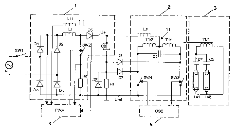
Figure 1 shows a block circuit diagram of an
electronic ballast having a rectifier,arrangement which is
connected to power supply voltage and feeds a stabilized DC
voltage to a connected inverter which, for its part,
supplies a lamp load circuit with a high-frequency pulse
train, the rectifier arrangement being assigned a circuit
for inrush current limiting in the form of a resistor
arranged in its output stage,
Figures 2, 3 in each case show a further
embodiment of
CA 02276913 1999-07-06
- 6 -
the electronic ballast according to Figure
1, the circuit for inrush current limiting
in each case having a switching transistor
whose switching path is connected in
parallel with the non-reactive resistor.
Figure 1 illustrates a block circuit diagram of an
electronic ballast for fluorescent lamps, in which a
rectifier arrangement 1 is connected, on the input side,
to AC power supply voltage u via a conventional power
supply switch SW1. This voltage is rectified by means of a
rectifier bridge comprising diodes Dl to D4. A charging
inductor L1 and also a forward-biased charging diode D5
are serially connected to an output of said rectifier
bridge which is at high potential. The output of the
rectifier bridge Dl to D4 which is at low potential is
connected to housing ground. A defined reference potential
Uref for the entire electronic ballast is thus
established. On the cathode side, the charging diode D5 is
connected to a storage capacitor C2, whose second terminal
is connected to reference potential Uref, as will be
explained in detail below.
Furthermore, a series circuit comprising the switching
path of a second switch, preferably an electronic switch
SW2, and a non-reactive resistor RO is arranged between
the junction point between charging inductor L1 and
charging diode D5, on the one hand, and the reference
potential Uref, on the other hand. This second switch SW2
forms the switching element of a step-up converter of the
rectifier arrangement 1. The function of this second
switch SW2 is controlled by means of a control unit 4. The
inputs thereof are respectively connected to the output of
the rectifier bridge Dl to D4 which is at high potential,
to an auxiliary winding L11 assigned to the charging
inductor L1, to the junction point between the second
CA 02276913 1999-07-06
- 7 -
switch SW2 and the resistor RO connected in series with
the latter, and to the terminal of the storage capacitor
C2 which is at high potential. On the output side, this
control unit 4 is connected to the control input of the
second switch SW2.
The rectifier arrangement 1 described above constitutes an
inherently known basic circuit of an AC/DC voltage
converter with active step-up converter for an electronic
ballast. All that is needed, therefore, is a summarizing
description of function, as given below. When the power
supply switch SW1 is closed, a pulsating DC voltage is
output at the outputs of the rectifier bridge Dl to D4.
This voltage is to be converted into a stabilized DC
voltage U+ by means of the storage capacitor C2 forming
the output stage of the rectifier arrangement 1. In this
case, the voltage difference between the instantaneous
value of the power supply voltage u or the pulsating DC
voltage derived therefrom, on the one hand, and the
voltage across the storage capacitor C2, on the other
hand, is bridged by means of the second switch SW2. If the
latter is closed, the current in the charging inductor Ll
rises and is detected by means of the auxiliary winding
L11. When an envisaged final value is reached, the second
switch SW2 opens and the current discharges into the
storage capacitor C2. A precondition for this is that the
voltage across the storage capacitor C2 is always larger
than the power supply voltage u. As soon as this charging
current becomes zero, the second switch SW2 is switched on
again by means of the control unit 4 assigned to it, until
an envisaged desired value is reached. The instantaneous
value of the pulsating DC voltage serves as the desired
value in this case. Consequently, a defined charged state
of the storage capacitor C2 is achieved by means of this
circuit. The stabilized DC voltage U+ corresponding to its
charged state in this case corresponds to the peak value
CA 02276913 1999-07-06
- 8 -
of the pulsating DC voltage.
An inverter 2, which is in this case designed as a
transformer-controlled push-pull chopper, is connected to
the rectifier arrangement 1. It converts the stabilized DC
voltage U+ fed in by the rectifier arrangement 1 into a
high-frequency pulse train. In the case of the embodiment
illustrated in Figure 1, the output of the rectifier
arrangement 1 which is at high potential is connected, in
the inverter 2, via a second inductor L2 to the common
junction point between two primary windings T1/1 and T1/2
of an oscillatory transformer Tl. Second terminals of
these primary windings Tl/1 and T1/2 are connected, in the
first instance, to one another via a resonance capacitor
C1 which is connected in parallel with both of them.
Furthermore, these terminals are respectively connected to
the reference potential Uref via the switching path of one
of two further switches SW3 and SW4. A drive network 5 for
these two further switches SW3 and SW4 is specified
schematically in Figure 1; circuit details with respect to
said drive network are illustrated in the further Figures
2 and 3, as will be described below.
The basic circuit, illustrated in Figure 1, for the
inverter 2 with the symmetrically constructed oscillatory
transformer T1 is also inherently known; therefore, the
function of the inverter 2 shall be summarized as follows.
The drive unit 5 is designed such that it alternatively
switches on one of the two further switches SW3 and SW4.
If it is assumed that the switch SW3 is in the on state
with the switching path closed, then current flows via the
further inductor L2 and one primary winding T1/1 -
assigned to this instantaneously turned-on switch SW3 - of
the oscillatory transformer T1 back into the rectifier
arrangement 1. As a result, the resonance capacitor Ci is
charged at the same time, the voltage at the
CA 02276913 1999-07-06
- 9 -
instantaneously turned-off switch SW4 rising. With the
next control pulse of the drive unit 5, this switch SW4 is
switched on, the resonance capacitor Cl initially being
discharged and, on account of the current flow through the
second primary winding T1/2, being charged in the opposite
direction. As the figurative expressiveness is very apt,
the expression "push-pull" circuit has also been adopted
in German usage for a circuit of this type.
As is furthermore shown by Figure 1, a lamp load circuit 3
is inductively coupled to the inverter 2 via a secondary
winding T1/4 of the oscillatory transformer Ti. A bipolar
pulse train is coupled into the lamp load circuit 3 via
said inverter, the frequency of which pulse train is
predetermined by the switching periods of the two switches
SW3 and SW4 of the inverter 2. Merely by way of example,
two fluorescent lamps Lal, La2 are provided in the lamp
load circuit. In this case, one of the filaments of the
fluorescent lamps Lal and La2 in each case is connected
via a respective limiting capacitor C4 and C5 to one of
the terminals of the secondary winding T1/4. The other
filaments of the fluorescent lamps are jointly connected
directly to the second terminal of said secondary winding
T1/4,
Finally, a network assigned to the storage capacitor C2 is
furthermore illustrated in Figure 1. This network contains
a further non-reactive resistor R1, which is henceforth
referred to as a limiting resistor. This limiting
resistor, in series with the storage capacitor C2, is
connected to the return path into the rectifier arrange-
ment 1, said return path being at reference potential
Uref. The junction point between the storage capacitor C2
and the limiting resistor R1 is connected via a respective
coupling diode D6 and D7 to that terminal of the further
switches SW3 and SW4, respectively, which is connected to
CA 02276913 1999-07-06
- 10 -
the corresponding primary winding Tl/1 and T1/2,
respectively, of the oscillatory transformer Ti. A further
diode D8 is connected in parallel with the limiting
resistor R1.
The inrush current occurring in the electronic ballast
when the power supply switch SW1 is closed is limited by
this network. During this switch-on operation, the step-up
converter of the rectifier arrangement 1 and also the
inverter 2 start only with a delay, since the supply
voltages for the corresponding switches SW2 and SW3, SW4,
respectively, must first be built up. In this switch-on
phase, the storage capacitor C2 is charged to the pre-
determined value of the stabilized DC voltage U+. The
inrush current flowing in the process is limited by the
limiting resistor R1 connected in series with the storage
capacitor C2. As soon as the inverter 2 has started,
however, in each case one of its two switches SW3.and SW4
is alternately switched on. The storage capacitor C2 is
consequently connected to reference potential Uref via the
respectively turned-on switch SW3 or SW4 and the
respective coupling diode D6 or D7 connected to the
switching path of said switch. Consequently, in steady-
state operation, the charging current for the storage
capacitor C2 no longer flows via the limiting resistor R1
but rather, preferably, via a path connected in parallel
with the latter. The further diode D8 connected in
parallel with the limiting resistor Rl serves for the
controlled discharge of the storage capacitor C2 into the
inverter 2. This is the case when the energy instanta-
neously fed in from the power supply side no longer
suffices by itself to operate the inverter 2, this being
the case in the region of the zero crossings of the AC
power supply voltage u.
Figure 2 illustrates a further exemplary embodiment of the
CA 02276913 1999-07-06
- il -
electronic ballast. In terms of its essential
construction, this corresponds to the example already
explained above with reference to Figure 1. Identical
circuit elements are identified by identical reference
symbols. Only the differences from the exemplary embodi-
ment in accordance with Figure 1 will be discussed,
therefore, in the course of the further description.
First of all, the way in which it is possible to configure
the drive unit 5 for the two switches SW3 and SW4 of the
inverter 2 is shown in more detail in Figure 2. In order
to generate the supply voltages for these two switches SW3
and SW4 of the inverter 2, the oscillatory transformer T1
has a further secondary winding T1/3, one terminal of
which is connected directly to reference potential Uref.
Its second terminal is connected via a further charging
diode D9 to a second storage capacitor C3, which is
connected to reference potential Uref on the other hand.
The charge of this second storage capacitor C3 yields the
supply voltages for the two switches SW3 and SW4 of the
inverter 2, which are designed as transistor switches in
this exemplary embodiment. The base terminals of said
switches form the control inputs and are in each case
connected to one of the winding terminals of a further
secondary winding T1/5 of the oscillatory transformer T1,
on the one hand, and, via a respective further non-
reactive resistor R2 and R3, to the junction point between
the second storage capacitor C3 and the charging diode D9
assigned thereto. This junction point is connected via one
of these two resistors, R2 in the example, and a further
resistor R5 to that output of the rectifier arrangement 1
which supplies the stabilized DC voltage U+. In steady-
state operation, the secondary winding T1/5 connected to
the base terminals of the switches SW3 and SW4 of the
inverter 2 supplies the commutator voltage for alternative
activation of said two switches.
CA 02276913 1999-07-06
- 12 -
Furthermore, in the exemplary embodiment of Figure 2, the
two coupling diodes D6 and D7 of the exemplary embodiment
of Figure 1 are replaced by a further transistor switch
Ql, whose switching path is connected in parallel with the
limiting resistor R1. This further transistor switch Qi is
also connected via a base resistor R4 to the second
storage capacitor C3. Therefore, as soon as the second
storage capacitor C3 is sufficiently charged, that is to
say the operating state of the inverter 2 has been
reached, this further transistor switch Q1 is turned on
and short circuits the limiting resistor R1.
Figure 3 illustrates a further embodiment of the
electronic ballast, which differs from the exemplary
embodiment in Figure 2 merely with regard to the driving
of the further transistor switch Ql whose switching path
is connected in parallel with the limiting resistor Ri. In
the case of this alternative, the two emitters of the
transistor switches SW3, SW4 of the inverter 2 are
connected to the reference potential Uref via a clamping
diode D10. Furthermore, this diode is connected in
parallel with the emitter-base junction of the further
switching transistor Q1. In this exemplary embodiment,
too, the limiting resistor R1 ensures that the inrush
current is limited during the switch-on operation.
However, as soon as the inverter 2 has started, current
flows via the reciprocally switched-on transistor switches
SW3 and SW4, said current flowing via the clamping diode
D10. The voltage drop caused across the clamping diode D10
as a result of this switches on the further transistor
switch Q1, which, for its part, short circuits the
limiting resistor Ri.
The exemplary embodiments described above teach that a
simple and cost-effective solution for limiting the inrush
CA 02276913 1999-07-06
- 13 -
current can be realized in an electronic ballast with a
rectifier arrangement which supplies a stabilized DC
voltage by means of an active step-up converter. In this
case, it must merely be ensured that there is a constant
ground connection, i.e. conductive connection to the
reference potential, during operation. As explained, this
can be achieved by means of an inverter in a "push-pull"
circuit.