Note: Descriptions are shown in the official language in which they were submitted.
CA 02277187 1999-07-09
WO 99/25158 1 PCT/IB98/01670
Circuit arrangement.
The invention relates to a circuit arrangement for supplying a lamp with a
DC lamp current comprising only passive components and equipped with
_ mains input terminals for connection to poles of a supply voltage source,
_ rectifying means, equipped with two input terminals, coupled to the mains
input terminals, and two output terminals, for generating a DC voltage out of
a low
frequency AC voltage supplied by said supply voltage source,
_ capacitive means, coupled between the mains input terminals and the
output terminals of the rectifying means,
a load circuit coupled to the output terminals of the rectifying means and
comprising terminals for connection to the lamp, and
inductive means.
The invention also relates to a compact lamp.
A circuit arrangement as mentioned in the opening paragraph is known
from US 4,929,871. In the known circuit arrangement the inductive means and
the capacitive
means are arranged in series between one of the mains input terminals and one
of the input
terminals of the rectifying means that are formed by a diode bridge. The load
circuit contains
only the terminals for lamp connection. During operation the known circuit
arrangement
supplies a DC current to the load. The known circuit arrangement is relatively
simple and
therefore relatively cheap. An important disadvantage of the known circuit
arrangement,
however, is that during stationary operation the lamp current becomes zero in
every half
period of the low frequency AC voltage. As a result the lamp will extinguish
in every half
period of the low frequency supply voltage. In case the lamp is a discharge
lamp, it will
therefore have to be reignited in each half period of the low frequency supply
voltage. This
reduces the life of the lamp electrodes and also causes reignition losses.
The invention aims to provide a circuit arrangement for operating a lamp
that is relatively cheap and simple and does not have the disadvantages
mentioned hereabove.
CONFIt~111ATI0N COPY
CA 02277187 1999-07-09
WO 99/25158 2 PCT/IB98/01670
A circuit arrangement as mentioned in the opening paragraph is therefore
in accordance with the invention characterized in that the load circuit is
equipped with a
series arrangement connecting the output terminals of the rectifying means and
comprising
the inductive means and the terminals for connection to the lamp.
Since the inductive means are in series with the lamp during lamp
operation, the inductive means supplies the lamp with a "keep-alive current"
when the
voltage between the input terminals of the rectifying means is close to zero
Volt. This "keep-
alive current" flaws from a first terminal of the inductive means through the
rectifying means
and the lamp to a second terminal of the inductive means. The operation is
called continuous
operation, if the circuit arrangement is so dimensioned that the lamp current
never drops to
zero. Therefore, in case of continuous operation and in case the lamp is a
discharge lamp,
the lamp does not extinguish and need not be reignited every half period of
the supply
voltage. It be mentioned that the circuit can also be so dimensioned that the
keep alive
current becomes zero in the time lapse during which the voltage between the
input terminals
of the rectifying means is close to zero. This is called discontinuous
operation. The lamp, if
it is a discharge lamp, will extinguish and will have to be reignited every
half period of the
supply voltage. It has been found both for continuous as well as for
discontinuous operation
that the inductance of the inductive means and the capacitance of the
capacitive means in a
circuit arrangement according to the invention can be chosen considerably
smaller than in the
circuit arrangement disclosed in US 4,929,871. The circuit arrangement
according to the
invention can therefore be considerably less voluminous and weigh
substantially less than the
known circuit arrangement. Another important advantage over the prior art that
was found to
exist for continuous operation only is a fast ignition of the discharge lamp
without "pinking"
and with only relatively little sputtering of emitter material from the
electrode taking place.
Since the inductive means are only subjected to a DC current, the flux swing
and the core
losses in the inductive means are relatively small resulting in an efficient
operation of the
circuit arrangement.
Preferably the impedance of the capacitive means is higher than the
impedance of the inductive means. The capacitive means functions as a current
limiter, while
the inductive means supplies current to the lamp during at least part of the
time lapse during
which current is not supplied to the lamp by the supply voltage source.
Since, as explained hereabove) the inductance of the inductive means can
be relatively small, the inductive means may comprise a choke with a core of
compressed
iron powder. The inductive means can thus be realized in a relatively cheap
and simple way
CA 02277187 1999-07-09
WO 99125158 3 PCT/IB98101670
and the core can easily be manufactured in many different forms. This latter
aspect can be
very important in case the circuit arrangement is integrated in a compact
lamp, since it is
possible to choose a form of the core, such as for instance a thoroid) that
will easily fit into
the compact lamp and provides a good heat conduction from the circuit
arrangement into the
environment.
The rectifying means may comprise a diode bridge but alternatively the
rectifying means may comprise a voltage doubter. This is particularly usefull
in case the
amplitude of the low frequency supply voltage is relatively low. In case the
capacitive means
is formed by two capacitors comprised in the voltage doubter, these two
capacitors function
both as current limiter and as part of the voltage doubter, so that different
functions in the
circuit arrangement are realized using relatively few components. The
rectifying means can
also comprise both a diode bridge and a voltage doubter, the voltage doubter
comprising two
of the diodes of the diode bridge and two capacitors. The rectifying means
substantially
function as a voltage doubter at low loads, i. e. before the lamp operated by
means of the
circuit arrangement has ignited. This way a high enough ignition voltage is
realized, even in
case the amplitude of the low frequency AC voltage supplied by the supply
voltage source is
relatively low. After ignition of the lamp) when the load has increased, the
rectifying means
substantially function as a diode bridge.
Good results have been obtained with relatively simple embodiments of
the circuit arrangement according to the invention wherein the circuit
arrangement
exclusively comprises components that make up the capacitive means ) the
inductive means
and the rectifying means.
It has been found that a circuit arrangement according to the invention is
very suitable for operating both a low pressure discharge lamp such as a low
pressure
mercury discharge lamp as well as a high pressure discharge lamp such as a
Philips CDM
lamp. Since it comprises relatively few components and is therefore relatively
small, a circuit
arrangement according to the invention is very suitable to be used in a
compact lighting unit
comprising both a circuit arrangement according to the invention and either a
tow pressure
discharge lamp or a high pressure discharge lamp coupled with the circuit
arrangement.
More in particular a circuit arrangement according to the invention is very
suitable to be
used in the ballast means of a compact lamp comprising
- a light source provided with a vessel that is closed in a gastight manner
and transmissive for visible radiation,
- a housing connected to the light source and provided with a lamp cap,
CA 02277187 1999-07-09
wo 99~25t5s 4 rc~rns9sro16~o
ballast means electrically connected to the light source for operating the
light source and positioned at least partly in a space surrounded by the
housing.
Preferably the circuit arrangement is so dimensioned that the DC current
that flows through the light source during operation of the compact lamp is
continuous.
The light source of such a compact lamp can for instance be a low
pressure discharge lamp or a high pressure discharge lamp.
In case such a compact lamp is for instance a compact fluorescent lamp
and the light source contains mercury, it is very advantageous if the light
source comprises
an amalgam. It has been found that the amalgam compensates to a large extent
the effect of
cataphoresis, that takes place since the lamp is supplied with a DC-current.
Preferably the
amalgam contains lead, bismuth and tin or bismuth and indium.
Embodiments of the invention will be described making use of a drawing.
In the drawing Fig. 1 shows a schematic representation of a first embodiment
of a circuit
arrangement according to the invention with a discharge lamp connected to it;
Fig. 2 shows a schematic representation of a second embodiment of a
circuit arrangement according to the invention with a discharge lamp connected
to it;
Fig. 3 shows a schematic representation of a third embodiment of a circuit
arrangement according to the invention with a discharge lamp connected to it;
Fig. 4 shows a schematic representation of a compact fluorescent lamp
with an integrated circuit arrangement as shown in Fig. 1, and
Fig. 5 shows the lamp current as a function of time for a discharge lamp
operated by means of a circuit arrangement as shown in Fig. 1.
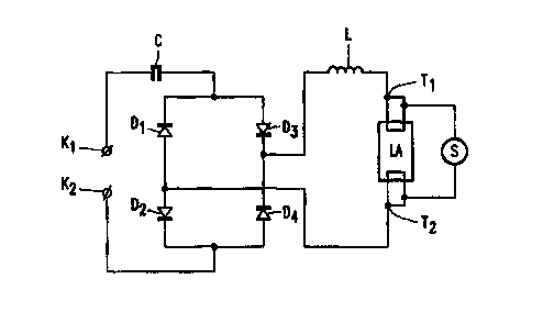
In Fig. 1 Kl and K2 are mains input terminals for connection to poles of
a supply voltage source. Mains input terminal Kl is connected by means of a
capacitor C to
a first input terminal of a rectifying means that in this embodiment is formed
by the diode
bridge D1-D4. Capacitor C forms the capacitive means in this embodiment. A
second input
terminal of the rectifying means is connected to mains input terminal K2.
Output terminals of
the rectifying means are connected by means of a series arrangement of choke L
and
terminals T1 and T2 for lamp connection. In the embodiment shown in Fig. 1
choke L forms
inductive means. A discharge lamp La is connected to terminals T1 and T2. The
discharge
lamp is shunted by a glow switch starter S.
The operation of the circuit arrangement shown in Fig. 1 is as follows.
When the poles of a supply voltage source supplying a low frequency AC
CA 02277187 1999-07-09
WO 99/25158 5 PCT/IB98/01670
voltage are connected to the mains input terminals KI and K2, the low
frequency AC voltage
is rectified by the diode bridge and a DC voltage is present between terminal
T1 and
terminal T2 causing a DC current to flow through the glow switch starter in
case the
discharge lamp has not yet ignited. This DC current can be used to preheat the
cathode of
the lamp. It has been found, however, that this is not always necessary. When
the glow
switch starter interrupts the DC current flowing through it, the choke
generates a relatively
high DC voltage between terminals T1 and T2 causing a breakdown in the lamp.
In case the
circuit arrangement is dimensioned for continuous operation it is capable of
supplying a
relatively large current immediately after breakdown. As a result a vapour arc
is generated
which can be sustained long enough for a stable hot spot to form on the
cathode. As a result
no glow discharge occurs during the ignition of the discharge lamp and
sputtering of lamp
electrode material is consequently substantially avoided. For this reason the
electrode life and
therefore the lamp life are strongly increased with respect to a lamp that is
ignited making
use of a AC voltage. Once the discharge lamp is ignited, a DC current flows
through both
the Lamp and choke L. This DC current can be described as the sum of a
constant DC
current and an AC current with a frequency that is twice the frequency of the
low frequency
AC voltage supplied by the supply voltage source. The dimensioning is such
that the
capacitor C functions as an impedance that Limits the DC current. The choke L
in this
embodiment comprises a thoroid of compressed iron powder. When the amplitude
of the
voltage between the input terminals of the diode bridge drops below the value
that is
necessary for the rectifying means to conduct a supply current from the supply
voltage
source to the lamp, the choke supplies a "keep-alive current" to the lamp.
This "keep-alive
current" flows from one end of the choke L through the lamp and all four
diodes back to the
other end of choke L. Choke L is preferably so dimensioned that the "keep-
alive current"
does not drop to zero in the time lapse during which the rectifying means are
not conducting
a supply current. Alternatively choke L can be so dimensioned that the "keep-
alive current"
does become zero only for a very short time in the time lapse during which the
rectifying
means are not conducting a supply current. In this latter case the lamp will
easily reignite
once the rectifying means are conducting the supply current again. In a
practical realization
of the embodiment shown in Fig. 1, the capacity of capacitor C was chosen at
2.2 ~F and
the inductance of choke L at 1.6 H. The supply voltage source supplied a
sinusoidal AC
voltage with a frequency of 50 Hz and an amplitude of 220 Volts rms. It was
found that the
circuit arrangement was very suitable for operating a low pressure mercury
discharge lamp
with a nominal power of 18 Watt and a burner voltage of approximately 80 Volt.
CA 02277187 1999-07-09
wo 99ns158 6 PCT/IB98101670
The shape of the lamp current of a low pressure mercury discharge lamp
operated by a circuit arrangement as shown in Fig. 1 is shown in Fig. 5. Along
the vertical
axis current is plotted in mA and long the horizontal axis time is plotted in
msec. It can be
seen that the current is the sum of a constant DC current and an AC current
with a frequency
that is twice the frequency of the low frequency AC voltage supplied by the
supply voltage
source. The constant DC current ( = the keep alive current) has an amplitude
that is equal to
the lowest value of the amplitude of the total lamp current. This amplitude is
shown in Fig. 5
as a horizontal line. Since the frequency of the supply voltage that was used
was 50 Hz, the
frequency of the AC current part of the lamp current is 100 Hz.
In Fig. 2 circuit parts that are similar to circuit parts in the embodiment
shown in Fig. 1 are labelled with the same symbols. The rectifying means in
this embodi-
ment are formed by a voltage doubler consisting of capacitors C 1 and C2 and
diodes D 1 and
D2. The capacitors C 1 and C2 are also the capacitive means in this
embodiment. The voltage
doubter comprises a first series arrangement of capacitors C 1 and C2. This
first series
arrangement is shunted by a second series arrangement of diodes D 1 and D2 and
by a third
series arrangement of a choke L and lamp connection terminals T i and T2. A
discharge lamp
La shunted by a glow switch starter S is connected to the terminals T 1 and
T2. Mains input
terminal K 1 is connected to a common terminal of diodes D 1 and D2. Mains
input terminal
K2 is connected to a common terminal of capacitors C 1 and C2. The maximum
output
voltage of the rectifying means in this embodiment (being the voltage over the
series
arrangement of capacitors C 1 and C2) is equal to twice the maximum amplitude
of the low
frequency supply voltage. In the embodiment shown in Fig. 1 the maximum output
voltage
of the rectifying means only equals the maximum amplitude of the low frequency
supply
voltage. The embodiment shown in Fig. 2 can offer advantages in case the
maximum
amplitude of the low frequency supply voltage is relatively low. Otherwise the
functioning of
the embodiment shown in Fig. 2 is similar to that of the embodiment shown in
Fig. 1 and
will not be described here in detail. In a practical realization of the
embodiment shown in
Fig. 2, the capacity of capacitors C1 and C2 was chosen at 3.9 ~.F and the
inductance of
choke L at 850 mH. The amplitude of the sinusoidal low frequency supply
voltage that was
used to supply the circuit arrangement was 120 Volt rms and its frequency was
60 Hz. It was
found that the circuit arrangement was very suitable for operating a low
pressure mercury
discharge lamp with a nominal power of 18 Watt and a burner voltage of
approximately 80
Volt.
In Fig. 3 circuit parts that are similar to circuit parts in the embodiment
CA 02277187 1999-07-09
WO 99/25158 ~ PCT/IB98/01670
shown in Fig. 1 are labelled with the same symbols. The rectifying means in
this embodi-
ment comprise both a diode bridge formed by diodes D 1-D4 and a voltage
doubler consisting
of capacitors C3 and C4 and diodes D2 and D4. Capacitors C3 and C4 shunt diode
D 1 and
diode D2 respectively. Apart from the presence of capacitors C3 and C4) the
embodiment
shown in Fig. 3 is similar to the embodiment shown in Fig. 1. The capacities
of capacitors
C3 and C4 are chosen substantially equal and much smaller than the capacity of
capacitor C.
Before ignition, when the load of the circuit arrangement is very small the
rectifying means
substantially function as a voltage doubter so that the voltage over the lamp
La is high
enough to ignite the lamp La. After ignition the rectifying means
substantially function as a
diode bridge and the functioning of the embodiment shown in Fig. 3 is the same
as the
functioning of the embodiment shown in Fig. 1.
In Fig. 4, a light source 8 is provided with a (discharge) vessel which is
closed in a gastight manner, is transmissive for radiation and comprises two
electrodes: an
anode and a cathode (not shown). It is remarked that the anode can be of a
particular simple
construction since it does not need to emit electrons. The light source
contains a filling
consisting of a mixture of noble gases. An amalgam A is present in the light
source in the
vicinity of the anode. A housing 6 is connected to the light source and
provided with a lamp
cap 3, in this embodiment that part of the housing that is below the broken
line A. This
housing may be formed, for example, from a synthetic resin. B is a circuit
arrangement as
shown in Fig. 1. Circuit arrangement B is electrically connected to the light
source. This
connection is indicated with broken lines 9 in Fig. 3. The circuit arrangement
B is placed in
a space 7 which is surrounded by the housing 6. E forms current conducting
connections
between the circuit arrangement B and metal contacts I and 2 placed on the
lamp cap. A
supply voltage is present between said contacts during lamp operation.
During lamp operation a DC current flows through the light source, which
results in a migration of mercury ions in the direction of the cathode of the
light source. This
process is known as cataphoresis and can result in a strong decrease in the
light output of the
light source because of the absence of mercury in a large part of the
discharge vessel. In the
compact lamp shown in Fig. 3, however, the migration of mercury ions towards
the cathode
by means of cataphoresis is compensated by the transport of mercury atoms
caused by the
amalgam in the vicinity of the anode. It has been found that the light output
of the light
source remained at a constant level, irrespective of the time during which the
lamp was kept
in operation.