Note: Descriptions are shown in the official language in which they were submitted.
CA 02277631 1999-07-16
1 WT 9 US
July 13, 1999
h
Transmission Channel for the Electrically Isolated
Transmission of Digital Signals
BACKGROUND OF THE INVENTION
This invention relates to a transmission channel for the
electrically isolated transmission of digital signals.
Prior-art transmission channels of this kind are
frequently used for the transmission of digital signals by
means of signal transmission lines, particularly over
great distances, and serve to separate the potentials
between the transmitter and receiver units of a data
communications system. Such potential isolation is
necessary to suppress interference signals caused by
transient currents on the signal transmission lines.
Because of their high efficiency, transformers are often
used to provide electrical isolation. Due to the effect of
the inductances of transformers, however, the use of the
latter reduces the edge steepness of the digital signal,
so that this method may be unsuitable. In addition,
transformers also transfer electromagnetic interference
introduced to them, and the suppression of such
interference involves a considerable amount of technical
complexity. DE-A 36 14 832, WO-A 89/12 366, and EP-A 198
263 each disclose a transmission channel for transmitting
digital signals
CA 02277631 1999-07-16
2 WT 9 US
July 13, 1999
- with a first digital-signal port for a first digital
signal to be transmitted and
- with~a second digital-signal port for a transmitted
second digital signal,
said transmission channel comprising:
- an isolating path with a predeterminable isolation
capability;
- a first conversion stage
-- with a coupling-signal port for a first coupling signal
transmissible across the isolating path; and
- a second conversion stage
-- with a coupling-signal port for a third coupling signal
transmissible across the isolating path,
- the isolating path being provided between a coil of the
first conversion stage and a coil of the second
conversion stage, and
- the second conversion stage converting the second
coupling signal to the second digital signal by means of
a flip-flop
-- having a set input coupled to the second coupling-signal
port and
-- having an output coupled to the second digital-signal
port.
If signals are to be transmitted between two
transmitter/receiver units, such electrically isolating
circuit arrangements must also be operable
bidirectionally, i.e., in a first and a second direction
of transmission. This is not possible with the prior-art
transmission channels described.
CA 02277631 2002-O1-24
78254-1
3
Another disa<~vantage associated with the use of
flip-flops in such transmission channels is that their on
state is not defined.
SUMMARY C.>E 'fHE INVENTION
It is therefore are obj ect c:~f the invention to
province a transmission channel. for tree electrically isolated
transmission of digital signals by means of transformers
wherein the direction of transmissior:. can be changed during
operation.
Another object is to provide a circuit arrangement
for t'ze electrically isolated transmission of digital
signals by means of a transformer 'wherein remains .in an
I5 unambiguous, static stage before and after the transmission
of a ~~igital signal. The digital signal transmitted by
means of this circuit arrangement is to have a sufficient
edge ateepness.
To attain this object, a first variant of the
invenv~ion provides a transmis~>ion channel for transmitting
digital signals with a Ei_rst digital-signal port for a first
digit<~1 signal to be tr.ansmi.tt:ed, and with a second digital-
signal port for a transmitted second digital signal, said
transmission channel comprising: an isolating path with a
predev:.erminable isolation capability; a first conversion
stage having a coupling--signal. port. for a first coupling
CA 02277631 2002-O1-24
78254-1
4
signal transmissible across the isolating path; and a second
conversion stage havincx a coupling-signal port for a third
coupling signal transmissible across the isolating path,
said .isolating path being provided between a first coil
disposed in the first c.onversi_on stage and a second coil
disposed in the second conver~>ion stage, each of s<~id coils
havin~~ a first and a second coil ternuinal, and said second
conversion stage conver-~,ing the second coupling signal to
the s~Jcond digital signal by means of a monostable
multivibrator, wherein the mul_tivibrator has a set input
coupled to the second coupling-signal port and an output
coupled to the second ci.igital--signal port.
A second variant of the invention provides a
transmission channel fo:r trap:>mitting digital signals in a
first direction settable during operation or in a second
direction settable during operation, with a deactivatable
first digital-signal port fc:~r a first digital. signal to be
transmitted, a deactivatable :>econd di.git.al-signal port for
a transmitted second digital. signal, a deactivatable third
digital-signal port for a t.hiz°d digital signal to be
transmitted, and a deactivatable fourth digital-signal port
for a transmitted fourt~:~ digital sigrua.l, said transmission
channel comprising: a single isolatirug path with a
predeterminable isolation capability; a first conversion
stage having a coupling-signa7_ port f:o:r a first coupling
CA 02277631 2002-O1-24
78254-1
signal transmissible across the isolating path cr for a
second coupling signal transmissible across the isolating
path; and a second conv~~r_sion stage having a coupling-signal
5 port for a third coupling signal trarrsmissibl.e across the
isolating path or for a f_our.th coupling signal transmissible
across the isolating path, :>aid isolatinq path being
provided between a first: coil disposed in the first
conversion stage and a second coil dz..sposed in the second
conversion stage, each of said coils having a first and a
second coil terminal, wherein the third digital-signal port
and t:ze fourth digital signal port are deactivated when the
first direction of transmission has been selected, and
wherein the first digit~a7_-signal port: and the second
digital-signal port are deactivated when the second
dire coon of transmission has been selected.
In a first embodiment of the first variant of the
invention, the multivib:rator comprises: a capacitor of
predeverminable capacitance having a first capacitor
terminal and a second capacitor terminal; a resistor of
predeverminable resistance having a first resistor terminal
conne~Jted to the second capacitor terminal and a second
resis'~or terminal connected to a reference potential; a
first inverter having an inverter .input connected to the
first coil terminal of t=he second coil and an inverter
outpui~ connected to the airst capacitor terminal; and a
second inverter having an inverter input connected to the
second capacitor terminal. and an irmerter output connected
to the second coil terminal of the second coil.
CA 02277631 2002-O1-24
78254-1
6
In a first embodiment of the second variant of the
invention, the transmission. channel- comprises: a first
selection-signal port for a first selection signal serving
to deactivate the first: digital-signal port or the third
digital-signal port; and a second selection-signal port for
a second selection signal serving to deactivate the second
digital-signal port or the fourth digital-signal port.
In a second embodiment of the second variant of
the invention, the transmission channel comprises: a first
tri-state buffer havin<~ an input coupled to the first
digital-signal port; a second tri-state buffer having an
output coupled to the second digital-signal port; a third
tri-state buffer having an input coupled to the third
digital-signal port; and a fourth tri-state buffer having an
output coupled to the fourth digital--signal port, wherein,
if the first direction of transmission has been selected,
the first and second tri-state buffers are in a low-
impedance state and the third and fourth tri-state buffers
are in a high-impedance state and wherein, if. the second
direction of transmission has been selected, the first and
second tri-state buffers are ~_n a hic:~h-impedance state and
the third and fourth t:ri-state buffers are in a low-
impedance state.
In a third ernbodi.ment of true second variant of the
invention, the second convers,'_on stage comprises a
multivibrator having at .Least one stable state.
CA 02277631 2002-O1-24
78254-1
7
In a fourth embodiment of t:he second variant of
the invention, the mul.1=ivibr_ator has two stable states.
In a fifth embodiment of true second variant of the
invention, the multivibratcr comprises a non-inverting
amplifier circuit having an input coupled to the first coil
terminal of the second coil and having an output coupled to
the second coil terminal of the second coil.
In a sixth embodiment of the second variant of the
invention, the multivitor_atc>r has a sz_ngle stable state.
In a second embodiment of the first variant of the
invention or in an eighth embodiment of the seccnd variant,
the first conversion stage comprises a delay circuit
providing a predeterminable delay and having an input fed by
the first digital signa~y and an outpa.zt coupled to 'the second
coil terminal of the f:i_rst cov~l.
In a ninth embodiment of the first second variant
of the invention, the delay c_~rcuit <:.omprises a tri-state
buffer.
In a third embodiment of the first variant of the
invention or in a tenth embod:~ment of the second variant, at
least one of the first coin>ling signal and the third
coupling signal is a three-va~aued logic signals.
In a fourth embodiment of the first variant of the
invention and in an eleventh embodiment of the second
variant, at least one of the first coupling signal and the
third coupling signal is a voltage appearing across the
first coil.
CA 02277631 2002-O1-24
78254-1
8
One advantage of thE: invention is that the edge
steepness of the transmitted digital signals is not reduced.
This means that the dic~.ital signals appearing at the output
of
CA 02277631 1999-07-16
9 WT 9 US
July 13, 1999
the circuit arrangement have the same edge steepness as
those applied at the input.
Another advantage of the invention is that because of the
reference potential at the respective switching stage, the
circuit arrangement has a defined~quiescent level, to
which it returns after each signal transmission.
BRIEF DESCRIPTION OF THE DRAWINGS
The invention and further advantages will become more
apparent from the following description of embodiments
when taken in conjunction with the accompanying drawings.
Throughout the figures, like parts are designated by like
reference characters. In the drawings:
Fig. 1 is a schematic block diagram of a transmission
channel for the electrically isolated
transmission of digital signals;
Fig. 2 is a schematic circuit diagram of the channel of
Fig. 1, comprising a monostable multivibrator;
Figs. 3a
to 3d and
Figs. 4a
to 4f show, byway of example, waveforms of different
potentials occurring during operation of the
channel of Fig. 2;
CA 02277631 1999-07-16
WT 9 US
July 13, 1999
Fig. 5 is a schematic block diagram of a transmission
channel for the electrically isolated,
bidirectional transmission of digital signals;
5 Fig. 6 is a schematic circuit diagram of a
bidirectional driver circuit for the
transmission channel of Fig. 5;
Fig. 7 is a schematic circuit diagram of another
10- bidirectional driver circuit for the
transmission channel of Fig. 5; and
Fig. 8 is a schematic circuit diagram of a further
bidirectional driver circuit for the
transmission channel of Fig. 5.
DETAILED DESCRIPTION OF PREFERRED EMBODIMENTS
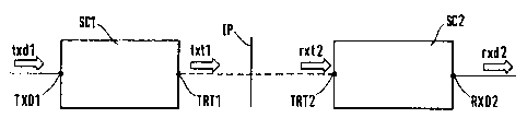
Fig. 1 shows a schematic block diagram of a transmission
channel for the electrically isolated transmission of
digital signals, particularly of binary signals, between a
first and a second transmitter/receiver unit (not shown)
in a selected direction of transmission. The digital
signal can be any two-valued electric signal of
predeterminable pulse width and pulse repetition rate and
of predeterminable mark-to-space ratio.
The transmission channel comprises a first digital-signal
port TXD1 for a first signal to be transmitted, txdl, and
CA 02277631 1999-07-16
11 WT 9 US
July 13, 1999
a second digital-signal port RXD2 for a transmitted second
digital signal rxd2.
The transmission channel further comprises a first
conversion stage SC1 with a coupling-signal port TRT1, a
second conversion stage SC2 with a coupling- signal port
TRT2, and an isolating path IP between the coupling-signal
ports TRT1~, TRT2, which has a predeterminable isolation
capability. The isolation capability of the isolating path
IP is dependent on dielectric strength and electric
conductivity. It increases with increasing dielectric
strength and/or decreasing conductivity.
The conversion stage SCl serves to convert the digital
signal txdl applied at the digital-signal port TXD1 to a
first coupling signal txtl, which appears at the coupling-
signal port TRT1 and is transmissible across the isolating
path IP. The conversion stage SC2 serves to convert a
second coupling signal rxt2, transmitted across the
isolating path IP and agplied at the coupling-signal port
TRT2, to the digital signal rxd2 appearing at the digital-
signal port RXD2.
Similarly, the isolating path IP, on the one hand, serves
to change the coupling signal txtl at the coupling-signal
port TRT1 into the coupling signal rxt2 at the coupling-
signal port TRT2. On the other hand, it also serves to
prevent interference signals caused, for example, by
potential differences along the transmission channel, from
getting into the coupling signal rxt2, and thus into the
digital signal rxd2.
CA 02277631 1999-07-16
' 12 WT 9 US
July 13, 1999
In the preferred embodiment shown in Fig. 2, the isolating
path IP is implemented by a transformer air gap between a
coil 2 of the conversion stage SC1, which serves as a
first transformer winding, and a coil 3 of the conversion
STAGE SC2, which serves as a second transformer winding;
if necessary, it can also be implemented, for example,
with an isolating path of a transformer embedded in
insulating material and/or with two or more successive
isolating paths of transformers connected in parallel.
The coil 2 has a first terminal 21 connected to a first
potential Upland a second terminal 22 connected to a second
potential U~" while the coil 3 has a first terminal 31
connected to a third potential U,land a second terminal 32
connected to a fourth potential U,1. The two coils 2, 3 are
so arranged relative to each other that during operation
of the transmission channel, a stray magnetic field
generated in one of the coils 2, 3 is coupled into the
respective other coil 3, 2. The coupling signals txtl,
txt2 can thus be time-varying current or voltage signals,
particularly pulse signals; cf. DE-A 36 14 832, WO-A 89/12
366, and EP-A 198 263.
During operation of the transmission channel, if the
digital signal txdl is fed in, the potentials U~1, U~Z, U,1,
U,Z have values which, as shown in Figs. 3a, 3b, 4e, and 4f,
are assigned to a first logic state H (high) and a second
logic state L (low). The H state covers a first range of
potential or voltage values which has a first upper limit
CA 02277631 1999-07-16
13 WT 9 US
July 13, 1999
Hoand a first lower limit H~. The L state covers a second
range of potential or voltage values which has a second
upper limit Loand a second lower limit L". The two ranges
of values do not overlap, i.e., the first lower limit H~ is
higher than the second upper limit Lp.
In one embodiment of the invention, the coupling signal
txtl is a first voltage U2 which, in operation, assumes
the H or L state or a third logic state -H with an upper
range limit -Ho, which is lower than the range limit L",
and with a lower range limit -H~; see Fig. 3c.
This logically three-valued voltage UZof predeterminable
pulse width is generated by means of the conversion stage
SC1. To do this, in operation, the potential Uzlis varied
with time in response to the directly applied digital
signal txdl, and the potential U~,is varied in response to
a digital signal derived from, and shifted in phase with
respect to, the digital signal txdl. To produce the phase
shift, the digital signal txdl is also applied to an input
of a noninverting delay circuit 4 providing a
predeterminable delay, and appears at an output of the
delay circuit 4 connected to the coil port 22. The
difference U,l-U,~of the two time-varying and out-of-phase
potentials U,1, Uz~ forms the voltage Uz see Fig. 3c. Figs.
3a and 3b show possible waveforms of the potentials Upland
U,z, respectively, which, for the sake of simplicity,
correspond to square-wave signals with a unity mark-to-
space ratio.
CA 02277631 1999-07-16
14 WT 9 US
July 13, 1999
For the delay circuit 4 of the conversion stage SC1,
virtually any delay chain of predeterminable gain and
predeterminable signal delay can be used, which can be
implemented, for example, with logic gates, cascaded
inverters, or noninverting operational amplifiers. The
gain of the delay chain must be chosen so that, if UZland
U~, are at the H level, the voltage UZassumes a value at
least equal to the lower range limit L~ and not exceeding
the upper range limit Laof the L state.
If a digital signal txdl with a resulting potential
waveform as shown in Fig. 3a or 3b is fed in, and the
delay chain has unity gain, the waveform of the voltage U,
shown in Fig. 3c is obtained, which corresponds to the
coupling signal txtl.
The delay of the delay circuit 4 must be chosen so that,
on the one hand, the pulse width of the voltage AU, ensures
reliable switching of the subsequent conversion stage SC2,
which receives the coupling signal rxd2, and that, on the
other hand, the signal potential U~~is shifted in phase
with respect to the signal potential U,~ by less than the
smallest expected pulse width of the digital signal txdl,
e.g., by 100 ns.
The voltage U" which serves as the coupling signal txtl,
is transmitted without a DC component from coil 2 to coil
3, where it appears in the form of a voltage U,as the
likewise three-valued coupling signal rxt2.
CA 02277631 1999-07-16
15 WT 9 US
July 13, 1999
Since the waveforms of the potentials U~" U22, at the two
primary-coil ports 21, 22 are the same for all
interference signals entering the transmission channel
after the delay circuit of the conversion stage SC1, an
interference-potential difference UZ* of a possible
interference signal is zero, i.e., such interference is
suppressed.
To convert the coupling signal rxt2 to the digital signal
rxd2, the conversion stage SC2 comprises a monostable
multivibrator 5 with a set input coupled to the coil port
31 and with a noninverting output coupled to the digital-
signal port RXD2; the digital-signal port RXD2 can also be
formed with an inverting output of the multivibrator 5
followed, if necessary, by a further inverter. Monostable
multivibrators, as is well known, have only one stable
state, namely either the H state or the L state, from
which they can be triggered to change the state for a
presettable interval; after this interval, they return to
the stable state.
This monostable multivibrator 5 serves to set a potential
U~o~ at the digital-signal port RXD2 to the H state on a
positive-going edge of the coupling signal rxt2
corresponding to a positive-going edge of the digital
signal txdl, and to the L state on a negative-going edge
of the coupling signal rxt2 corresponding to a negative-
going edge of the digital signal txdl, see Fig. 3d;
positive-going edges are changes of potential from one
state to a higher state, such as the change from L to H or
CA 02277631 1999-07-16
16 WT 9 US
July 13, 1999
from -H to L; negative-going edges are changes of
potential from one state to a lower state, such as the
change from H to L or from L to -H.
The waveform of the potential U~p~, except for a small
delay-induced phase shift and a possible interchange of
the sign, then corresponds to that of the digital signal
txdl, and thus to a mapping of the digital signal txdl
onto the digital signal rxd2.
In another prefered embodiment of the invention, as shown
in Fig. 2, the monostable multivibrator 5 comprises a
first inverter 51 with an input coupled to the coil
terminal 31, a second inverter 52 with an output coupled
to the coil terminal 32, a capacitor 53 with a first
terminal 531 coupled to an output of the inverter 52 and
with a second terminal 532 coupled to an input of the
inverter 52, and a resistor 54 with a first terminal
coupled to the input of the inverter 52 and with a second
terminal tied to a fixed reference potential U8, whose
value corresponds to the H state.
The input of the inverter 51 thus serves as the set input
of the multivibrator 5. Its output forms the inverting
output of the multivibrator 5, and the output of the
inverter 52 forms the noninverting output.
The capacitor 53 and the resistor 54 together act as a
memory circuit. This memory circuit serves to assign the L
state to a potential at an output of the memory circuit on
CA 02277631 1999-07-16
17 WT 9 US
July 13, 1999
a negative-going edge at an input of the memory circuit,
and to temporarily maintain this state. Further, the
memory circuit serves to assign the H state to the
potential at the memory output on a positive-going edge at
the memory input. Thus, this memory circuit makes it
possible to set an on time of the multivibrator 5 which is
equal to one pulse width of an H state at the noninverting
output of the multivibrator 5.
In the embodiment of Fig. 2, the memory input corresponds
to the capacitor port 531, while the memory output
corresponds to the capacitor port 532. A time constant T
proportional to a maximum on time, which is equal to the
product of capacitance C and resistance R, must be chosen
so that this maximum on time is approximately five times
greater than the greatest expected pulse width of the
digital signal txdl; it must be at least equal to the
expected pulse width. For a maximum pulse width of 1 ms
and a resistance value R of, e.g., 47 kS~, a capacitance C
of approximately 100 nF is obtained in the embodiment of
Fig. 2.
The operation of the monostable multivibrator 5 will now
be explained in more detail with reference to Figs. 4a to
4f.
In a first static state from a time toto a time t1, no
digital signal txdl is transmitted. Accordingly, both coil
ports 31, 32 are in the L state and the voltage AU, is
zero, see Figs. 4a, e, and f.
CA 02277631 1999-07-16
18 WT 9 US
July 13, 1999
Thus, both capacitor ports 531, 532 are at the reference
potential UB and thus remain in the H state, as shown in
Figs. 4b and c. Therefore, a capacitor voltage U53equal to
the difference between a potential US,lat the capacitor
port 531 and a potential US,Zat the capacitor 532 is also
zero, see Fig. 4d. Consequently, the capacitor 53 is
discharged.
On application of the digital signal txdl with a positive-
going edge at a time teas shown in Fig. 3a, the potential
U,lat the coil port 31 changes from zero to a higher value
corresponding to the H state.
As a result, the capacitor potential US,~. delayed by a
propagation delay through the inverter 51 with respect to
the positive-going edge, is set to a value for the L
state. Because of the integrating action of the capacitor
53 with respect to the capacitor voltage U5" the
capacitor port 532 immediately assumes the capacitor
potential US,z, which is zero. Again with a delay equal to
the propagation delay, the output of the inverter 52
changes to the H state. The multivibrator 5 is now in a
second state, which lasts from the time tlto a time t~.
During the second state, the capacitor 53 is slowly
charged according to an e-function determined by the time
constant T. As a result, the capacitor potential US,z
approaches the reference potential UB again. The greater
the time constant T is chosen, the more slowly the
CA 02277631 1999-07-16
19 WT 9 US
July 13, 1999
capacitor 53 will become charged and the more slowly the
capacitor potential US,zwill increase.
According to the predetermined delay introduced by the
delay circuit of the conversion stage SC1, the voltage U~
across the two coil ports 21, 22 is nonzero for only a
short time. When the voltage U~changes to zero at the
time t=, the potential U,lat the coil terminal 31 is held
at the value of the potential U3~at the coil terminal 32,
which, because of the slow charging of the capacitor 53,
is still in the H state.
Thus, the capacitor terminal 531 remains in the L state,
and the capacitor 53 continues to be charged. The
capacitor voltage Us, also approaches a value corresponding
to the reference potential Ue according to the above-
described e-function. From the time tZto a time t3, the
multivibrator 5 is in a third state. The time between tz
and t,corresponds to the on time of the monostable
multivibrator 5.
After a time corresponding to the pulse width of the
digital signal to be transmitted, at instant t" the
potential U,lat the coil terminal 31 changes from the H
state to a lower value corresponding to the L state;
accordingly, the capacitor potential US,lchanges to the
reference potential UB, i.e., the H state.
A momentary difference between the capacitor potential U5,1
and the capacitor potential US" is again compensated for
CA 02277631 1999-07-16
20 WT 9 US
July 13, 1999
practically without delay, so that the input of the second
inverter 52 immediately assumes the reference potential UH
and the capacitor 53 is discharged again. Thus, from the
time t,to a time t" the multivibrator 5 is in a fourth
state.
On the subsequent change of the voltage U~from the value
for the H state to zero, at the time t" the multivibrator
5 changes to a fifth state, which lasts until a time t5.
During the fifth state, analogously the third state, the
coil gort 31 is at the potential U,~of the coil port 32,
which is equal to the reference potential Ue.
The waveforms of the potentials 0531 / U" . and U,l appearing
at the outputs of the inverters 51, 52 and at the input of
the inverter 51, respectively, correspond to the waveform
of the digital signal to be transmitted, txdl, as far as
the order and the time distances between the positive-
going and negative-going edges are concerned, with the
potential US,lat the output of the inverter 51 representing
the waveform of the digital signal txdl with opposite
signs, i.e., practically to a digital signal -rxdl, which
can be readily changed into the digital signal rxdl by
subsequent inversion.
As the digital-signal port RXD2 can assume only one stable
state, after termination or abnormal termination of the
signal transmission, the transmission channel changes to a
defined output state or quiescent state.
CA 02277631 1999-07-16
21 WT 9 US
July 13, 1999
As shown in Fig. 2, the coil terminal 21 is connected
directly to the digital-signal port TXD1, and the coil
terminal 31 is connected practically directly to the
digital-signal port RXD2. If the set input of the
multivibrator 5 is coupled to the coil terminal 32, and
the noninverting output of the multivibrator 5 is coupled
to the coil terminal 31, an additional phase shift of the
digital signal rxd2 with respect to the digital signal
txdl is obtained, which is due to the fact that instead of
the edges of the coupling signal rxt2 corresponding to the
edges of the digital signal txdl, only the edges of the
coupling signal rxt2 corresponding to the respective edges
of the digital signal at the output of the delay circuit 4
now trigger or reset the multivibrator 5.
The delay provided by the delay circuit 4 must be at least
equal to a delay with which a change of the potential U,lat
the set input of the multivibrator 5 causes a change of
the potential U,Z .
The required quality of the electrical isolation of the
transmission channel is determined essentially by the
design of the transformer, and can thus be guaranteed in a
simple manner and over a wide range of application.
Another advantage is that no special-purpose components
are necessary, so that high transmission reliability can
be achieved at low cost.
According to a second variant of the invention, the
transmission channel serves to transmit digital signals,
CA 02277631 1999-07-16
22 WT 9 US
July 13, 1999
e.g., for the purpose of data communication, between a
first and a second transmitter/receiver unit (not shown)
in a selectable first direction or a selectable second
direction, providing electrical isolation. The digital
signal can again be any two-valued electric signal of
predeterminable pulse width and pulse repetition rate and
of predeterminable mark-to-space ratio.
As the transmission channel for transmitting the digital
signals operates bidirectionally in a half-duplex mode,
i.e., as it permits transmission in only one direction at
a time, it can be used, for example, to implement
potential-separated serial interfaces of microprocessor
systems or modems.
As shown in Fig. 5, the transmission channel for half-
duplex operation comprises a first deactivatable digital-
signal port TXD1' for a first digital signal to be
transmitted, txdl', a second deactivatable digital-signal
port RXD2' for a transmitted second digital signal rxd2',
a third deactivatable digital-signal port TXD2' for a
third digital signal to be transmitted, txd2', and a
fourth deactivatable digital-signal port RXD1' for a
transmitted fourth digital signal rxdl'. " Deactivatable"
as used herein means that, on application of suitable
control signals, the respective digital-signal port can
assume, besides an active, signal- passing state, an
inactive, signal-blocking state.
CA 02277631 1999-07-16
23 wT 9 vs
July 13, 1999
The transmission channel further comprises a first
selection signal port RXA1' for a binary first selection
signal rxal' serving to activate or deactivate the
digital-signal ports TXD1', RXD1' as well as a second
selection signal port RXA2' for a binary second selection
signal rxa2' serving to activate or deactivate the
digital-signal ports TXD2', RXD2'.
In the second variant of the invention, the first
direction of transmission of the transmission channel is
set by activating the two digital-signal ports TXD1',
RXD2' and deactivating the two digital-signal ports RXD1',
TXD2'. Similarly, the second direction of transmission is
set by activating the digital-signal ports TXD2', RXD1'
and deactivating the digital-signal ports RXD2', TXD1'.
" Deactivated" means that the respective digital-signal
port has a signal- blocking effect, i.e., that a digital
signal appearing at such a port is not passed to
subsequent circuit components of the transmission signal
or to the connected transmitter/receiver unit;
" activated" means that signals appearing at the
respective digital-signal port are passed. The activatable
and deactivatable digital-signal ports TXD1', TXD2',
TXD2', RXD1' can be implemented with all circuits familiar
to those skilled in the art which can be set to a signal-
passing state and a signal- blocking state in response to
corresponding control signals, such as driver circuits
implemented with open collector outputs or with tri-state
buffers.
CA 02277631 1999-07-16
- 24 WT 9 US
July 13, 1999
To implement the deactivatable digital-signal ports, in
another embodiment of the invention, shown in Fig. 7, the
transmission channel comprises a first tri-state buffer
61', a second tri-state buffer 62', a third tri-state
buffer 63', and a fourth tri-state buffer 64'. Tri-state
buffers, as is well known, are circuit elements which can
be set very quickly to a high-impedance, signal-blocking
state or a low-impedance, signal-passing state by
application of a binary selection signal to an additional
selecting input En. Thus, a change of a signal potential
applied at the input end of the tri-state buffer will
cause a corresponding change of a signal potential
appearing at the output end of the buffer only if the
buffer is in the active state; if the buffer is in the
inactive state, the signal potential appearing at the
output end will be unaffected by the signal potential at
the input end. Tri-state buffers of the kind described can
be both inverting and noninverting circuit elements.
As shown in Fig. 7, one input of the buffer 61' serves as
the digital-signal port TXD1', and an output of the buffer
62' serves as the digital-signal port RXD2'. One input of
the buffer 63' serves as the digital-signal port TXD2',
and an output of the buffer 64' serves as the digital-
signal port RXD1'. Furthermore, in the embodiment of Fig.
7, the selection signal ports RXA1' and RXA2' are
implemented by a noninverting port of the buffer 61'
coupled to an inverting port of the buffer 62' and by a
noninverting port of the buffer 63' coupled to an
inverting port of the buffer 64'. The selection signals
CA 02277631 1999-07-16
25 WT 9 US
July 13, 1999
rxal', rxa2' for selecting the first or second direction
of transmission must be implemented in such a way that the
tri-state buffers 63' and 64' are in a high-impedance,
i.e., signal-blocking, condition if the first direction of
transmission has been selected, and that the tri-state
buffers 61' and 62' are in a high-impedance condition if
the second direction of transmission has been selected.
For the transmission of the digital signals txdl', txd2',
the transmission channel of Fig. 5 further comprises a
first conversion stage SC1' with a coupling-signal port
TRT1' and a second conversion stage SC2' with a coupling-
signal port TRT2' as well as a single isolating path IP'
coupled between the coupling-signal ports TRTl', TRT2' and
having a predeterminable isolation capability.
If the first direction of transmission has been selected,
the conversion stage SC1' serves to convert the digital
signal txdl' to a first coupling signal txtl', which
appears at the coupling-signal port TRT1' and is
transmissible across the isolating path IP', and the
conversion stage SC2' serves to convert a second coupling
signal rxt2', transmitted across the isolating path IP'
and applied at the coupling-signal port TRT2', to the
digital signal rxd2'. If the second direction of the
transmission has been selected, the conversion stage SC2'
serves to convert the digital signal txd2' to a third
coupling signal txt2', which appears at the coupling-
signal port TRT2' and is transmissible across the
isolating path IP', and the conversion stage SC1' serves
CA 02277631 1999-07-16
26 WT 9 US
~ July 13, 1999
to convert a fourth coupling signal rxtl', transmitted
across the isolating path IP' and applied at the coupling-
signal port TRT1', to the digital signal rxdl'.
Similarly, the isolating path IP', besides suppressing
interference signals as mentioned above, serves to change
the coupling signal txtl' into the coupling signal rxt2'
applied at the coupling-signal port TRT2' if the first
direction of transmission has been selected, and to change
the coupling signal txt2' into the coupling signal rxtl'
applied at the coupling-signal port TRT1' if the second
direction of transmission has been selected.
In one embodiment of the second variant of the invention,
the isolating path IP', analogously to the first variant
of the invention, is a transformer air gap between a coil
2' of the conversion stage SC1', which serves as a first
transformer winding, and a coil 3' of the conversion stage
SC2', which serves as a second transformer winding, as
shown in Fig. 6; it can also be implemented with a
transformer embedded in insulating material and/or with
transformers connected in series, as mentioned above.
The coil 2' has a first terminal 21' connected to a first
potential UZland a second terminal 22' connected to a
second potential UzZsimilarly, the coil 3' has a first
terminal 31' connected to a third potential U,land a
terminal second port 32' connected to a fourth potential
U3z .
CA 02277631 1999-07-16
27 WT 9 US
July 13, 1999
In a further embodiment of the second variant of the
invention, as shown in Fig. 6, for the first direction of
transmission, the conversion stage SC1' comprises a delay
circuit 4' which serves to derive a phase-shifted digital
signal from the digital signal txdl' in the manner
described above. This digital signal is applied to the
coil port 32' and thus causes a change of the potential
U,z. The digital signal txdl' is also applied directly to
the coil port 31', so that a logically three-valued
voltage equal to a difference U,1 - U,zappears across the
coil 3'.
As in the case of the conversion stage SC1, noninverting
delay chains with a predeterminable delay can be used for
the delay circuit 4' of the conversion stage SC1'.
If the delay circuit 4' is to be switchable into and out
of circuit in operation, in a preferred embodiment, it
includes at least one tri-state buffer 41'.
Furthermore, the conversion stage SC2' comprises, at least
for the first direction of transmission, a multivibrator
5' for converting the coupling signal rxt2' to the digital
signal rxd2'. The multivibrator 5' has a set input coupled
to the coil port 31' and an output, particularly a
noninverting output, coupled to the digital-signal port
RXD2', and has at least one stable state. Similarly, for
the second direction of transmission, the conversion stage
SCl' may comprise a corresponding multivibrator (not
CA 02277631 1999-07-16
28 WT 9 US
July 13, 1999
shown) for converting the coupling signal rxtl' to the
digital signal rxdl'.
The multivibrator 5' again serves to assign the H state to
a potential U~pz' at the digital-signal port RXD2' on a
positive-going edge of the coupling signal rxtl'
associated with a positive-going edge of the digital
signal txdl', and the L state to the potential U~p2' on a
negative-going edge of the coupling signal rxt2'
associated with a negative-voing edge of the digital
signal txd2'.
In a further embodiment of the invention, for the first
direction of transmission, the time variation of the
potential U~o~' is realized by implementing the
multivibrator 5' of the conversion stage SC2' as a flip-
flop, which can assume two stable states, cf., for
example, DE-A 36 14 832, WO-A 89/12366; of course, a flip-
flop may also be included in the conversion stage SC1' for
changing the potential U~pz' if the second direction of
transmission has been selected.
In a further embodiment of the invention, the tri-state
buffer 62, as shown in Fig. 8, serves as a flip-flop 5' of
the conversion state SC2' for the first direction of
transmission. To this end, the tri-state buffer 62 is
implemented as a noninverting tri-state buffer whose input
and output are connected directly to the coil ports 31'
and 32', respectively. Similarly, a noninverting tri-state
buffer 64 having its input and output connected directly
CA 02277631 1999-07-16
29 WT 9 US
July 13, 1999
to the coil ports 22' and 21', respectively, may serve as
a flip-flop of the conversion stage SC1'.
In another embodiment of the invention, for the first
direction of transmission, the time variation of the
potential URXOZ' is realized by implementing the
multivibrator 5' of the conversion stage SC2' as a
monostable multivibrator, particularly in the manner of
the multivibrator 5 of the first variant of the invention,
shown in Fig. 2.
If the multivibrator 5 is used for the second variant of
the invention, the inverters 51, 52 of Fig. 2 can also be
implemented as inverting tri-state buffers, which can be
enabled by the selection signal r~a2', for example.
By means of the deactivated or activated digital-signal
ports TXD1', RXD1', TXD2', RXD2', the first and second
directions of transmission are set in such a manner that
the transmission of digital signals corresponding to a
direction not set would be blocked. To avoid any loss of
data in such a data exchange, the data to be transmitted
have to be stored temporarily, e.g. in a shift register,
and the setting of the directions of transmission must be
coordinated with the transmission of the respective
digital signals in a suitable manner, e.g. by clock
control and/or event control. This can be done in a
master-slave mode, for example.
CA 02277631 1999-07-16
30 WT 9 US
July 13, 1999
In transmission channels operated in this way, the event-
driven setting of the directions of transmission by means
of the selection signals rxal', rxa2' is accomplished
using corresponding digital control signals which have
predetermined control-bit sequenences, particularly in
accordance with a standardized interface protocol. To
generate the selection signals rxal', rxa2', these control
signals are transmitted ahead of and, if necessary, after
the digital signals txdl', txd2', so they can also be
transmitted across the isolating path.
The control signals and the selection signals rxal', rxa2'
can be generated using any of the control circuits for
such a serial data exchange which are familiar to those
skilled in the art, such as bus controllers or modem
controllers, as well as corresponding control methods,
e.g., methods implemented in a microprocessor; the control
circuits can be incorporated directly in the transmission
channel or in at least one of the transmitter/receiver
units, for example. If the transmission channel is used in
a bus system, each of the digital-signal ports TXD1',
RXD2', TXD2', RXD1' must be assigned a corresponding
distinguishable bus address and the above-mentioned
control circuit must incorporate suitable address control
means. Furthermore, the selection-signal ports RXA1',
RXA2' must be connected to a corresponding address bus.
The control signals may be carried, for example, on
additional, separate control lines originating from the
control circuit; they can also be implemented as a
CA 02277631 1999-07-16
31 WT 9 US
July 13, 1999
control-bit sequence preceding and, if necessary,
following the data bits of the digital signals to be
transmitted, as is commonly done in such serial
interfaces, and thus can be fed to the transmission
channel like the corresponding digital signal.
In a further embodiment of the invention, therefore, the
transmission channel also serves to transmit digital
control signals between a first and a second control
circuit (not shown).
In a further embodiment of the second variant of the
invention, the first control circuit is connected to the
digital-signal port TXD1', RXD1', and the second control
circuit is connected to the digital-signal ports TXD2',
RXD2', with each of the digital-signal ports TXD1', RXD2',
TXD2', RXD1' being acivated in an initial state of the
transmission channel. At a point of time prior to the
application of the digital signal txdl', the digital-
signal port TXD1' is fed with a digital first control
signal txcl' which is then converted, in the manner
described above, into a transmitted digital second control
signal rxc2' appearing at the digital-signal port RXD2'.
The control signal rxc2' is fed to the second control
circuit, which derives therefrom the selection signal
rxa2' and any further digital control signal to be
transmitted to the first control circuit. Similarly, at a
point of time prior to the application of the digital
signal txd2', the digital- signal port TXD2' is supplied
with a digital third control signal txc2', which is
CA 02277631 1999-07-16
32 WT 9 US
July 13, 1999
converted to a transmitted digital fourth control signal
rxcl' appearing at the digital-signal port RXD1'. The
control signal rxcl' is fed to the first control circuit,
which derives therefrom the selection signal rxal' and any
further digital control signal to be transmitted to the
second control circuit.
The transmission channel may, of course, have additional
control-signal ports, which are connected to separate
control lines. The control signals can also be fed to
further conversion stages in a corresponding manner.