Note: Descriptions are shown in the official language in which they were submitted.
CA 02277905 1999-07-12
SPECIFICATION
Non Contact Type IC Card
Technical Field
The present invention relates to a non contact type IC card, and more
particularly to a non contact type IC card allowing the protection of data
stored in the card and the prevention of data falsification.
Background Art
A non contact type IC card performing data communication with an
interrogator installed outside has been used conventionally. The examples
include a ticket for ski lift, a seasonal ticket for the transportation and a
prepaid card.
Fig. 7 is a block diagram schematically showing a basic structure of a
conventional non contact type IC card 900. Conventional non contact type
IC card 900 shown herein, which is an IC card performing data
communication in a signal superposing manner, supplies power and
transmits/receives information using a signals) having one or more
frequencies received from the interrogator not shown.
Conventional non contact type IC card 900 as shown in Fig. 7 is an
example of non contact type IC cards utilizing a single frequency and
includes a tuning circuit 20, a rectifying circuit 21, an
amplifying/demodulating circuit 22, a modulating/amplifying circuit 23 and
an SP/PS conversion circuit 24.
Tuning circuit 20 includes a coil L functioning as an antenna and a
capacitor C0. Rectifying circuit 21 rectifies a signal received at tuning
circuit 20, thereby generates and supplies the power to each part of non
contact type IC card 900.
Amplifying/demodulating circuit 22 amplifies and demodulates data
(a from an interrogator received at tuning circuit 20. A signal output from
amplifying/demodulating circuit 22 is SP-converted by SP/PS conversion
circuit 24 and then is output to a main control circuit 2 described below.
-1-
CA 02277905 1999-07-12
With reference to Fig. 7, conventional non contact type IC card 900
further includes main control circuit 2 and a memory 1.
Main control circuit 2 processes a signal output from SP/PS
conversion circuit 24. Main control circuit 2 generates data DA to be
stored in memory 1 described below and designates a location (adcliess) of
memory 1 to which data DA is to be written.
Memory 1 includes normal data storage region B1 and data
protection region B2. Memory 1 receives data DA via a data line L2 as
well as an address signal AD via an address line L1 indicating an address
(a location to which data is to be written) to which data DA is to be wiztten.
Here, data stored in data protection region B2 particularly requires
secuuty in order to guarantee a normal data communication and whose
rewriting is inhibited. An example of such data is an ID number of an ID
card holding the personal information.
In addition, main control circuit 2 reads data from designated region
B1 or data protection region B2 of memory 1 according to the contents of
data ~l received from the interrogator and generates a response data A
based on the read data. Response data A is PS-converted at SP/PS
conversion circuit 24, processed at modulating/amplifying circuit 23 and
then transmitted to the interrogator via coil L forming the antenna.
In conventional non contact type IC card 900, however, the rewriting
(falsification) of stored data in memory 1 can be easily performed from a
device other than the interrogator once the protocol of the data
communication with the interrogator is decoded, therefore the security
cannot be guar anteed.
Hence an object of the present invention is to provide a non contact
type IC card allowing the prevention of rewriting of a storage region in
which data requiizng security is stored.
Another object of the present invention is to provide a highly reliable
non contact type IC card through the control of rewriting of the storage
region in which data requiring security is stored.
Disclosure of the Invention
-2-
CA 02277905 2001-11-26
A non contact type IC card performing a data communication function based on
an externally applied radio wave signal includes; receiving means receiving
said radio
wave signal; a rectifying circuit connected to said receiving means; first
storing means
storing said data requiring security; second storing means storing data other
than said
data to be stored in said first storing means; control means generating said
data based on
the radio wave signal received at said receiving means and controlling for
writing said
data into a location in one of said first storing means and said second
storing means
according to a content of said generated data; detection means detecting a
frequency of
the radio wave signal received by said receiving means; and selection means
selecting
whether said data is to be written into said location in said first storing
means designated
by said control means based on a result of the detection by said detection
means; wherein
when said receiving means receives said radio wave signal and the frequency of
said
radio wave signal is detected to be a first frequency by said detection means,
said data is
written into said location in said first storing means designated by said
control means,
whereas when the frequency of said radio wave signal is detected to be a
second
frequency other than said first frequency by said detection means, said data
is not wmtten
into said location in said first storing means designated by said control
means.
According to another aspect of the invention a non contact type IC card
responsive to externally applied data for performing data communication
includes; first
storing means storing said data requiring security; second storing means
storing data
other than said data to be stored in said first storing means; control means
controlling for
writing said data into a location in one of said first storing means and said
second storing
means according to a content of said data; and data fixing means receiving
said data to be
written into said location in said first storing means designated by said
control means and
supplying a particular data; wherein only said particular data supplied from
said data
-3-
CA 02277905 2001-11-26
fixing means is written into said location in said first storing means
designated by said
control means, and wherein a value of said particular dat<~ supplied from said
data fixing
means is a value determined by an initial state of said first storing means.
According to another aspect of the invention a non contact type IC card
responsive to externally applied data for performing data communication
includes; first
storing means storing said data requiring security; second storing means
storing data
other than said data to be stored in said first storing means; control means
controlling for
writing said data into a location in one of said first storing means and said
second storing
means according to a content of said data; selection means selecting whether
said data is
to be written into said location in said first storing means designated by
said control
means; and state setting means controlling the selection by said selection
means; wherein
said data is written into said location in said first storing means designated
by said
control means when said state setting means is in a first state, whereas, said
data is
written into a location other than said location m saia first storing means
designated by
said control means when said state setting means is in a second state other
than the first
state.
-4 -
CA 02277905 2001-11-26
Therefore a main advantage of the present invention lies in the prevention of
falsification of storage contents through the control of rewriting of data
stored in a
storage portion storing data requiring security.
Brief Description of the Drawings
Fig. 1 shows a structure of a main portion of a non contact type IC card 100
according to a first embodiment.
Fig. 2 shows a structure of a main portion of a non contact type IC card 200
according to a second embodiment.
-5-
CA 02277905 2001-11-26
Fig. 3 shows a structure of a main portion of a non contact tvnP T(
card 300 according to a third embodiment .
Fig. 4 shows a structure of a main portion of a non contact type IC
card 400 according to a fourth embodiment
Fig. 5 shows a structure of a main portion of a non contact twe IC
card 500 according to a fifth embocliment .
Fig. 6 shows a structure of a main portion of a non contact type IC
card 600 according to a sixth embodiment .
Fig. 7 is a diagram schematically showing a structure of a
conventional non contact type IC card 900.
First Embodiment . --
The first embodiment allows the prevention of rewriting of data previously
stored
I5 ' in data protection region by
cnnfvohing an address to which data is to be written, at data writing for the
data protection region of a memory in a non contact type IC card.
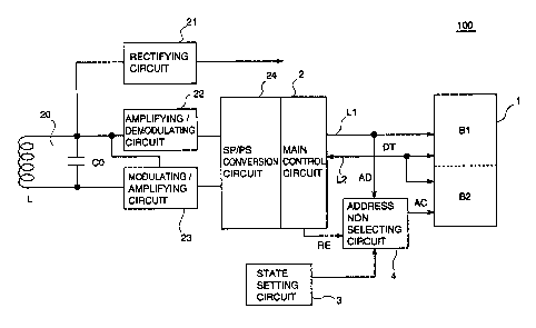
Fig. 1 shows a structure of a~ main portion of a non contact type IC
card 100 according to the first embodiment
Components similar to those in conventional non contact type IC card 900
shown in Fig. 7 are denoted by the same reference numbers and same
reference characters and the description thereof will not be repeated.
Here, data transmission of the non contact type IC card adopting the
present invention may be either in a signal superposing method or in a
signal separating method.
Non contact type IC card 100 shown in Fig. 1 differs from
conventional non contact type IC card 900 in that card 100 includes a state
setting circuit 3 and an adcliess non selecting circuit 4 controlling a write
address designated at data waiting for data protection region B2 of memory
1.
With reference to Fig. 1, the structure of non contact type IC caW
100 according to the first embodiment will be described.
-s-
CA 02277905 2001-11-26
Address non selecting circuit 4 receives a write enable signal RE
supplied from main control circuit 2 and an address signal AD from an
adcliess line L1 as inputs. Here, address signal AD designates a location
in data protection region B2 to which data DT on a data line L2 is to be
written, and write enable signal RE designates a data writing operation to
data protection region B2. Adcliess non selecting circuit 4 being controlled
by state setting circuit 3 described below outputs an address selecting
signal AC according to address signal AD.
State setting circuit 3 controls adcliess non selecting circuit 4
described above.
Address selecting signal AC output from address non selecting circuit
4 changes its state based on a state (active statelinactive state) of state
setting circuit 3. Specifically, when state setting circuit 3 is in an active
state, an output address selecting signal AC selects a location designated
by address AD as a location to which data is to be written, whereas when
state setting circuit 3 is in an inactive state, an output address selecting
signal AC inhibits the writing to the location designated by address signal
AD (non select state).
Data DT will be written into a location in data protection region B2
corresponding to and based on address selecting signal AC output from
adcliess non selecting circuit 4.
w
Next, an operation o~,non contact tvnP If', r~a,-~ inn according to the
first embodiment will be described.
First, when state setting circuit 3 is in an active state, adcliess non
selecting circuit 4 having received write enable signal RE and address
signal AD outputs adcliess selecting signal AC selecting a location
designated by the address signal AD. In this case data DT will be wiztten
into the corresponding location in data protection region B2.
On the other hand, when stage setting circuit 3 is in an inactive state,
address non selecting circuit 4 having received write enable signal RE and
address signal AD outputs address selecting aignal AC turning the location
designated by the address signal AD to a non select state. In this case
data DT is not written into data protection region B2.
_7_
CA 02277905 2001-11-26
One example of such state setting circuit 3 uses a fuse. For example,
when a fuse is used, any numbers of data can be written into data
protection region B2 before the fuse blow, however, after the fuse blow,
data in data protection region B2 can not be rewritten. The methods of
blowing the fuse includes high voltage application, laser cutting, induction
heating or the like.
In other words, by controlling the state of state setting circuit 3, non
contact type IC card 100 can inhibit t~e access to data protection region B2
for data revcnzting after the data requiring security is stored in data
protection region B2 (for simplicity this state is referred to as protection
data storage state).
Thus in non contact type IC card 100, as the address selection for the
data protection region can be controlled at the data writing operation, the
falsification of data previously stored in the data protection region can be
prevented.
Cn~.nnr~, ~!;ITl~?C)dlmel7.t
Similar to the first embodiment, the non contact type IC card according
to the second embodiment allows the prevention of rewriting of data stored in
the data
protection region by controlling an address to which the data is to be
written at the time of data writing to the data protection region in the
memory.
. Fig. 2 shows a structure of a main norti~n of a nnn ~nntart tvnP IC
card 200 according to the second embodiment and
components similar to those in non contact type IC card 10.0 shown in Fig
are denoted by the same reference numbers and same reference characters
and the description thereof will not be repeated.
Non contact type IC card 200 shown in Fig. 2 is different from
conventional non contact type IC card 900 in that it includes a command
detection circuit 5 and an adcliess non selecting circuit 6 controlling a
designated address to which data is to be written at the time of data
writing to the data protection region of the memory, and controls these
circuits by a command output frorn., a main control circuit 12.
_g_
CA 02277905 2001-11-26
With reference to Fig. 2, the structure of non contact type IC card
200 according to the second embodiment will now be described.
Address non selecting circuit G receives an address signal AD via an
address line L1 as an input. Here, address signal AD indicates a location
in data protection region B2 to which data DT on a data line L2 is to be
written. Address non selecting circuit 6 controlled by command detection
circuit 5 described below outputs adcliess selecting signal AC according to
the address signal AD.
Command detection circuit 5 receives a~n address control command
COM output from riiain control circuit 12 and controls address non
selecting circuit 6. Here, adcliess control command COM is a command
permitting or inhibiting a data writing operation to data protection region
B2 based on the address signal AD.
Address selecting' signal AC output from address non selecting circuit
G changes its state according to a state of command detection circuit 5.
Specifically, when command detection circuit 5 detects a writing permitted
state of a data protection region B2, an address selecting signal AC
selecting a location designated by address AD as a location to which data is
to be wiztten is output. On the other hand, ijE data protection region B2 is
detected to be in a writing inhibited state, address selecting signal AC
turning a location designated by adcliess signal AD to a non select state is
output.
Based on the address selecting signal A,C supplied fiom adcliess non
selecting circuit 6, data DT is written into a corresponding location in data
protection region B2.
Next an operation of non contact type IC card 200 according to the
second embodiment will be described.
When an adcliess control command COM permitting the data writing
is supplied from main control circuit 12, and is detected by command
detection circuit 5, address non selecting circuit 6 outputs an adcliess
selecting signal AC selecting a location designated by the adcliess signal
AD. In this case data DT is written into a corresponding location in data
_g_
CA 02277905 2001-11-26
protection region B2.
On the other hand, when an address control command COM
inhibiting the data writing is supplied from main control circuit 12, and is
detected by command detection circuit 5, address non selecting circuit 6
outputs an address selecting signal AC turning the location designated by
the address signal AD to a non select state. In this case data DT is not
written into data protection region B2.
Thus, non contact type IC card 200 allows the adjustment of storage
of data requiring security in data protection region B2 (turning data
protection region B2 to the protection data storage state) and inhibiting the
access to data protection region B2 for the data rewriting, through the
control of command detection circuit 5 based on a command output from
main. control circuit 12.
As non contact type IC card 200 allows the control of selection of
address of the data protection region at the data writing operation, the
falsification of data previously stored in the data protection region can be
prevented.
Third Embodiment
The third embodiment allows the prevention
of rewizting of data once stored in the data protection region in the non
contact type IC card through the access control for the data protection
region according to the frequency for data communication.
Fig. 3 shows a structure of a main portion of a non contact type IC
card 300 according to the third embodiment,
wherein components similar to those in non contact type IC card 100 shown
in Fig. 1 are denoted by the same reference numbers and same reference
characters, and the description thereof will not be repeated.
Non contact type IC card 300 shown in Fig. 3 is different from
conventional non contact type IC card 900 in that it includes a frequency
detection circuit 7 and an address non selecting circuit 8.
With reference to Fig. 3, the structure o~f non contact type IC card
300 according to the third embodiment will now be described.
10-
CA 02277905 1999-07-12
Frequency detection circuit 7 detects a frequency of a radio wave
received by tuning circuit 20 and includes a band pass filter and a
switching circuit inside not shown. When a caxmier frequency of a received
radio wave is a predetermined frequency F1, frequency detection circuit 7
detects the reception of an intended radio wave.
Address non selecting circuit 8 receives address signal AD via
address line L1 and a write enable signal RE from main control circuit 2 as
inputs. Here, adcliess signal AD designates a location in data protection
region B2 to which data DT on data line L2 is to be written.
Address non selecting circuit 8 controlled by frequency detection
circuit 7 outputs address selecting signal AC according to address signal
AD. More specifically, when frequency detection circuit 7 detects the
reception of an intended radio wave (with predetermined frequency F1), an
address selecting signal AC selecting a location designated by address
signal AD as a location to which data is to be written is output, and
otherwise (when received radio wave has a frequency other than the
predetermined frequency F1), an address selecting signal AC turning the
location designated by the address signal AD to a non select state is output.
Based on the address selecting signal AC, data DT is written into the
corresponding location in data protection region B2.
With reference to Fig. 3, an operation of non contact type IC card 300
will be described specifically.
As descxzbed above, when a radio wave with a carrier frequency F1 is
received, adcliess non selecting circuit 8 outputs an address selecting signal
AC selecting a location designated by address signal AD. In this case data
DT is written into the corresponding location in data protection region B2.
On the other hand, when a radio wave with a carrier frequency being
an oxzginal frequency FO different from F1 is received, address non
selecting circuit 8 outputs an address selecting signal AC turning the
location designated by address signal AD to a non select state. In this case
data DT is not written into data protection region B2.
In other words, non contact type IC card 300 allows the adjustment
of the storage of data requiring security in data protection region B2
-11-
CA 02277905 2001-11-26
(turning data protection region B2 to the protection data storage state) and
inhibiting the access to data protection region B2 for the data rewriting,
through the use of different frequencies.
Thus, as a non contact type IC card 300 allows the access control for
the data protection region according to the frequency of radio wave for the
data communication, the falsification of data previously stored in the data
protection region can be prevented.
Fourth Embodiment
The fourth embodiment allows the
prevention of data falsification, which is the object of the present
invention,
in the non contact type IC card by controlling the data to be written at the
data writing to the data protection region in the memory.
Fig. 4 shows a tructure of a main portion of a non contact type IC
card 400 according to' the fourth embodiment,
wheuein components similaa~ tQ those in ~.on contact type IC card 100 shown
in Fig. 1 are denoted by the same reference numbers and same reference
characters, and the description thereof will not be repeated.
Non contact type IC card 400 shown in Fig. 4 is different from
conventional non contact type IC card 900 in lthat it includes an input data
fixing circuit 9 controlling data to be written into data protection region B2
of memory 1.
With reference to Fig. 4, the structure of non contact type IC card
400 according to the fourth embodiment will be described.
Input data fixing circuit 9 fixes a state of each location in data
protection region B2 of memory 1.
Input data fixing circuit 9 receives data DT1 via a data line L2 as an
input, converts data DT1 and outputs data DT2. Data DT2 is data to be
w~~itten into data protection region B2.
A value of data DT2 output fiom input data fixing circuit 9 is
determined based on an initial state of data protection region B2. When
states of all bits in data protection region B2 are "1", for example, data DT2
always takes a value of the reverse polarity, in this case "0". Hence, when
-12-
CA 02277905 2001-11-26
main control circuit 2 outputs data DT1 corresponding to the value "1", the
data writing to data protection region B2 will not be performed.
With reference to Fig. 4, an operation of non contact type IC card 400
will be descubed specifically.
Assume that an initial state of each bit in data protection region B2
in memory 1 is set to "1" (the state of bit to "1111"). In this case, input
data fixing circuit 9 receiving data DT1 outputs only the data DT2 of "0" for
each bit.
First, data requiring security will be written into data protection
IO region B2 (protection data storage state). Here, assume that the
protection data storage state is "1100". As described above, data DT2
output fiom input data fixing circuit 9 takes the value "0". Therefore, the
bit once takes the state "0" cannot be returned to the state "1". As a result,
thereafter, the state of data protection region B2 (" 1100") cannot be
'.5 ''eWrltten to "1101", for exaanple.
Thus, data protection region B2 of non contact type IC card 400
functions as an OTP ROM (a non volatile memory allowing only one
rewlzting) and once data is stored in the data. protection region, teal of the
data rewriting is highly likely to result in a failure of an intended data
20 setting.
Thus, as desclzbed above, as non contact type IC card 400 allows the
control of data to be written into the data protection region at the data
wlzting operation, the rerouting of data once stored in the data protection
region can be prevented.
25 Fifth Embodiment
The fifth embodiment allows the preventr.on
of data falsification, which is the object of the present invention, in the
non
contact type IC card, by controlling an address to which data is to be
written at the data wizting operation to the data protection region of the
30 memory. ,
Fia. 5 shows a structure of a main portion of a non contact type IC
card 500 according to the fifth embodiment, '
wherein components similar to those in non contact type IC card 100 shown
- 13-
CA 02277905 2001-11-26
in Fig. 1 are denoted by the same reference numbers and same reference
characters, and the descuption thereof will not be repeated.
Non contact type IC card 500 shown in Fig. 5, is different from
conventional non contact type IC card 900 in that it includes a state setting
circuit 10 and an address non selecting circuil; 11 controlling a designated
adcliess to which data is to be wi~tten at the writing to data protection
region B2 of memory 1.
With reference to Fig. 5, the structure of non contact type IC card
500 according to the fifth embodiment will be described.
I0
Address non selecting circuit 11 receives a write enable signal RE
output from main control circuit 2 and address signal AD via address lime
L1 as inputs. Here, adcliess signal AD designates a location in data
protection region B2 to which data DT on data line L2 is to be wiztten.
? 5 Adcliess non selecting circuit 11 controlled by state setting ci~~cuit 10
described below, outputs adcliess selecting signal AC according to address
signal A,D.
State setting circuit 10 controls address non selecting circuit 11
described above.
20 Address selecting signal AC output from adcliess non selecting circuit
11 changes its state according to a state (active state/inactive state) of
state
setting circuit 10. More specifically, when state setting circuit 10 is in an
active state, address selecting signal AC selecting a location designated by
address signal AD as a location to which data is to be written is output, and
25 when state setting circuit 10 is in an inactive state, address selecting
signal
AC selecting a location other than the location designated by address signal
AD (or selecting neither of the location) is output.
Based on the address selecting signal A,C output from address non
selecting circuit 11, data DT is wiZtten into the corresponding location in
30 data protection region B2.
Next, an operation of non contact tyre IC card 500 accordine to the
fifth embodiment will be described.
First, when state setting circuit 10 is in. an active state, address non
- 14-
CA 02277905 2001-11-26
selecting circuit 11 having received write enable signal RE and adcliess
signal AD outputs an address selecting signal AC selecting a location
designated by adcliess signal AD. In this case, data DT is written into the
corresponding location in data protection region B2.
On the other hand, when state setting circuit 10 is in an inactive
state, adcliess non selecting circuit 11 having received write enable signal
RE and adcliess signal AD outputs an adcliess selecting signal AC selecting
a location other than the location designated by address signal AD (qr
selecting neither of the locations). In this case, data DT is not written into
the intended location of data protection region B2.
As described above, an example of such state settingEcircuit 10
includes a fuse.
Thus even if the rewriting operation occurs, non contact type IC card
500 can inhibit the rewriting of the intended data, after the data requiring
secuz~ity is stored in data protection region B2 (protection data storage
state), by controlling the state of state setting circuit 10.
Thus, as non contact type IC card 500 allows the control of adcliess
selection in the data protection region at the data writing operation,
rewriting and use of the data previously stored in the data protection
region can be prevented.
Sixth Embodiment
According to the sixth embodiment, a non
coxatact type IC card includes an OTP ROM (an non volatile memory
allowing only one rewriting) as a storage medium corresponding to the data
protection region.
Fig. 6 shows a structure of a main uortion of a non contact tune IC
card 600 according to the sixth embodiment,
wherein components similar to those in non contact type IC card 100 shown
in Fig. 1 are denoted by the same reference characters and the description
thereof will not be repeated.
Non contact type IC card 600 shown in Fig. 6 is different fiom
conventional non contact type IC card 900 in that it includes a memory 15
and a memory 16 instead of memory' 1.
- 15-
CA 02277905 2001-11-26
With reference to Fig. G, the structure of non contact type IC card
600 according to the sixth embodiment will be described.
Memory 15 is a storage medium storing' rewntable data whereas
meu~ory 16 is a storage meclium storing data requiring the security.
Specifically, memory 15 includes a non volatile memory allowing
rewriting as required such as an EEPROM and a flash memory, whereas
memory 16 includes a memory allqwing only one rewriting such as an
EPROM.
Next, an operation of no-n contact. type IC card 600 according to the
sixtH embodiment will be described. For - ,
simplicity, in the description, memory 16 is assumed to be an EPROM.
Data to be held that is output from main control circuit 2 is stored in
mex~ory 15 or memory 16.
In this case, as memory 1G is an EPROM, once electa~ic charge is
stored in a memory cell not shown, the electric: charge cannot be discharged
until it is exposed to ultraviolet light. Therefore, assuming that the state
of a memory cell with electric charge stored is called state 1 and the
discharged state of the memory cell is called state 0, after the encapsulation
of IC~ card G00, in memory 1G, a memory cell iti the state 0 can be charged to
be tl~e state 1, however, a memory cell in the state 1 cannot be rewritten to
be tl~e state 0.
Therefore, it is highly unlikely that the teal of rewuting of data once
stored in memory 1G achieves the intended data rewriting.
Thus, with the use of an OTPROM as a medium for storing data to
be protected, non contact type IC card G00 allows the suppression of data
falsification to an extremely low level.
As can be seen from the foregoing, according to the present invention,
the rewriting of storage region in which data requiring the security is
stored can be prevented through the control of data rewuting.
In addition, according to the present invention, as the rewriting can
be controlled with respect to the storage region in which data requiring the
secuuty is stored, the reliability of the non contact type IC card can be
-16-
<IMG>