Note: Descriptions are shown in the official language in which they were submitted.
CA 02278308 1999-07-20
WO 98/33218 PCT/US98/00843
SEMICONDUCTOR DIODES HAVING LOW FORWARD
CONDUCTION VOLTAGE DROP AND LOW REVERSE
CURRENT LEAKAGE
BACKGROUND OF THE INVENTION
1. Field of the Invention
The present invention relates to the field of
semiconductor devices and methods of fabricating the
same.
2. Prior Art
Semiconductor devices of various kinds are well
known in the prior art. The present invention relates
to methods of fabricating semiconductor diodes and the
diodes so fabricated, though the methods are also
directly applicable to the fabrication of transistors as
well. Because of the emphasis on diodes herein, only
the prior art relating thereto will be discussed.
Semiconductor diodes are widely used in electronic
circuits for various purposes. The primary purpose of
such semiconductor diodes is to provide conduction of
current in a forward direction in response to a forward
voltage bias, and to block conduction of current in the
reverse direction in response to a reverse voltage bias.
This rectifying function is widely used in such circuits
as power supplies of various kinds as well as in"many
other electronic circuits.
In typical semiconductor diodes, conduction in the
forward direction is limited to leakage current values
CA 02278308 1999-07-20 WO 98/33218 PCT/US98/00843
-2-
until the forward voltage bias reaches a characteristic
value for the particular type of semiconductor device.
By way of example, silicon pn junction diodes don't
conduct significantly until the forward bias voltage is
at least approximately 0.7 volts. Many silicon Schottky
diodes, because of the characteristics of the Schottky
barrier, can begin to conduct at lower voltages, such as
0.4 volts. Germanium pn junction diodes have a forward
conduction voltage drop of approximately 0.3 volts at
room temperature. However, the same are currently only
rarely used, not only because of their incompatibility
with silicon integrated circuit fabrication, but also
even as a discrete device because of temperature
sensitivity and other undesirable characteristics
thereof.
In some applications, diodes are used not for their
rectifying characteristics, but rather to be always
forward biased so as to provide their characteristic
forward conduction voltage drop. For instance, in
integrated circuits, diodes or diode connected
transistors are frequently used to provide a forward
conduction voltage drop substantially equal to the base-
emitter voltage of another transistor in the circuit.
While certain embodiments of the present invention may
find use in circuits of this general kind, such use is
not a primary objective thereof.
In circuits which utilize the true rectifying
characteristics of semiconductor diodes, the forward
conduction voltage drop of the diode is usually a
substantial disadvantage. By way of specific example,
in a DC to DC step-down converter, a transformer is
typically used wherein a semiconductor switch controlled
by an appropriate controller is used to periodically
connect and disconnect the primary of the transformer
CA 02278308 1999-07-20
WO 98/33218 PCT/US98/00843
-3-
with a DC power source. The secondary voltage is
connected to a converter output, either through-a diode
for its rectifying characteristics, or through another
semiconductor switch. The controller varies either the
duty cycle or the frequency of the primary connection to
the power source as required to maintain the desired
output voltage. If a semiconductor switch is used to
connect the secondary to the output, the operation of
this second switch is also controlled by the controller.
Use of a semiconductor switch to couple the
secondary to the output has the advantage of a very low
forward conduction voltage drop, though has the
disadvantage of requiring careful control throughout the
operating temperature range of the converter to maintain
the efficiency of the energy transfer from primary to
secondary. The use of a semiconductor diode for this
purpose has the advantage of eliminating the need for
control of a secondary switch, but has the disadvantage
of imposing the forward conduction voltage drop of the
semiconductor diode on the secondary circuit. This has
at least two very substantial disadvantages. First, the
forward conduction voltage drop of the semiconductor
device can substantially reduce the efficiency of the
converter. For instance, the newer integrated circuits
commonly used in computer systems are going to lower and
lower operating voltages, such as currently 3.3 volts, 3
volts and a-s low as 2.7 volts. In a 3 volt power
supply, the imposition of a 0.7 volt series voltage drop
means that the converter is in effect operating into a
3.7 volt load, thereby limiting the efficiency of the
converter to 81%, even before other circuit losses are
considered.
Second, the efficiency loss described above
represents a power loss in the diode, resulting in the
CA 02278308 1999-07-20
WO 98/33218 PCTIUS98/00843
-4-
heating thereof. This limits the power conversion
capability of an integrated circuit converter, and in
many applications would require the use of a discreet
diode of adequate size, increasing the overall circuit
size and cost.
Another commonly used circuit for AC to DC
conversion is the full wave bridge rectifier usually
coupled to the_secondary winding of. a transformer having
the primary thereof driven by the AC power source. Here
two diode voltage drops are imposed on the peak DC
output, making the circuit particularly inefficient
using conventional diodes, and increasing the heat
generation of the circuit requiring dissipation through
large discrete devices, heat dissipating structures,
etc. depending on the DC power to be provided.
Therefore, it would be highly advantageous to have
a semiconductor diode having a low forward conduction
voltage drop for use as a rectifying element in circuits
wherein the diode will be subjected to both forward and
reverse bias voltages from time to time. While such a
diode may find many applications in discreet form, it
would be further desirable for such a diode to be
compatible with integrated circuit fabrication
techniques so that the same could be realized in
integrated circuit form as part of a much larger
integrated circuit. Further, while reverse current
leakage is always undesirable and normally must be made
up by additional forward conduction current, thereby
decreasing circuit efficiency, reverse current leakage
can have other and more substantial deleterious _aLffects
on some circuits. Accordingly it would also be
desirable for such a semiconductor diode to further have
a low reverse bias leakage current.
CA 02278308 2001-06-26
-5-
SUMMARY OF THE INVENTION
Semiconductor diodes having a low forward voltage
conduction drop, a low reverse leakage current and a high
voltage capability suitable for use in integrated circuits
as well as for discrete devices are disclosed. The
semiconductor diodes are fabricated as field effect
devices having a common gate and drain connection by a
process which provides very short channels, shallow drain
regions and longitudinally graded junctions. Continuation
of the gate/drain contact layer over specially located,
tapered edge field oxide maximizes the breakdown voltage
of the devices. The preferred fabrication technique
utilizes four masking steps, all without any critical mask
alignment requirements. Various embodiments are
disclosed.
In one aspect, the present invention provides a
rectifying circuit having first and second diode
connections comprisinq a circuit wherein a diode is
subjected to positive and negative differential voltages
between the first and second diode connections to provide
a rectified output; the diode having source, gate and
drain regions, the dra_Ln and gate regions being
electrically interconnected by a common conductive layer
forming the first diode connection, a semiconductor
substrate of a first conductivity type having first and
second surfaces and forming one of the diode connections;
a plurality of pedestals on the first surface of the
substrate; a first oxide layer on the substrate between
pedestals; the pedestals having side regions thereon with
a channel region in the substrate below the first oxide
layer under the side regions and on the first surface of
CA 02278308 2005-09-07
-5a-
the substrate; the substrate having a buried layer of a
second conductivity type under and between the side
regions; and, a conductive layer forming the other diode
connection and electrically connecting the side regions on
the pedestals and the substrate between the side regions.
In one embodiment, the diode is a power level diode.
In a still further aspect, the present invention
provides a rectifying circuit having first and second
diode connections comprising: a circuit wherein the diode
is subjected to positive and negative differential
voltages between the first and second diode connections to
provide a rectified output; the diode having source, gate
and drain regions, the drain and gate regions being
electrically interconnected by a common conductive layer
forming the first diode connection; the diode having: a
semiconductor substrate of a first conductivity type
having first and second surfaces and forming one of the
diode connections; a plurality of pedestals on the first
surface of the substrate; a first oxide layer on the
substrate between pedestals; the pedestals having side
regions thereon with a channel region in the substrate
below the first oxide layer under the side regions and on
the first surface of the substrate; the substrate having a
buried layer of a second conductivity type under and
between the side regions; a conductive layer forming the
other diode connection and electrically connecting the
side regions on the pedestals and the substrate between
the side regions; a second oxide layer on the substrate,
the second oxide layer surrounding the area of the first
surface of the substrate having the plurality of pedestals
thereon and being tapered to a minimum thickness at an
edge thereof facing the plurality of pedestals, the
conductive layer extending over the tapered edge of the
CA 02278308 2001-06-26
-5b-
oxide, the buried layer extending to the first surface and
terminating in the region of the tapered oxide; the
conductive layer beinq in electrical contact with the
buried layer in selected regions between pedestals.
BRIEF DESCRIPTION OF' THE FIGURES
Figure 1 is a circuit diagram for a well known AC to
DC converter using a full wave bridge rectifier in which
the present invention may be used.
Figures 2a and 2b illustrate diode connected field
effect devices, shown schematically in as n-channel and p-
channel diode connected field effect devices, in
accordance with the px-esent invention.
Figures 3a throuqh 3v illustrate steps in an
exemplary process for fabricating a preferred embodiment
of the present invention.
Figures 3w and 3x illustrate steps in an alternate
process for fabricatiriq the present invention.
CA 02278308 1999-07-20
WO 98/33218 PCT/US98/00843
-6-
Figure 4 is a reproduction of a computer simulation
of the field lines on both sides of the pn junction and
in the oxide when the preferred embodiment of the
present invention is subjected to a reverse bias of 80
volts.
Figures 5a through 5c illustrate a further
exemplary alternate method of fabrication for the
present invention.
DETAILED DESCRIPTION OF THE PRESENT INVENTION
First referring to Figure 1, a circuit diagram for
a well known AC to DC converter using a full wave bridge
rectifier in which the present invention may be used may
be seen. In such circuits, a transformer 20 is used to
provide DC isolation between the primary and secondary
circuits and frequently to provide an AC voltage step-up
or step-down to the full wave bridge, comprised of
diodes Dl, D2, D3 and D4. When the secondary lead 22 is
sufficiently positive with respect to secondary lead 24,
diode D2 will conduct through resister 26 to charge or
further charge capacitor 28 and to provide current to
load 30, which current returns to lead 24 of the
transformer through diode D3. Similarly, during the
other half cycle of the AC input voltage, when the
voltage on secondary lead 24 is sufficiently positive
with respect to secondary lead 22, diode D4 will conduct
to provide current through resistor 26 to charge
capacitor 28 and to provide current to load 30, with the
capacitor and load currents being returned to thZ
secondary lead 22 through diode Dl. Thus it may be seen
that each time current is delivered from the full wave
bridge of diodes Dl through D4 to the output of the
bridge, two diode voltage drops are imposed in series
CA 02278308 1999-07-20
WO 98/33218 PCT/US98/00843
-7-
with that output. Further, since any pair of diodes
conduct only when the voltage across the secondary of
the transformer 20 exceeds the voltage across capacitor
28 by two diode voltage drops, it is clear that current
is delivered to the output of the bridge only during a
fraction of the time, namely when the transformer
secondary voltage is at or near a positive or negative
peak.
The circuit of Figure 1 is merely exemplary of the
type of circuit in which the present invention is
intended to be used. These circuits may be
characterized as circuits wherein the diode will be
subjected to both positive (forward) and negative
(reverse) differential voltages across the two diode
connections and the function of the diode is a
rectifying function to provide a DC or rectified current
output. This is to be distinguished from applications
wherein the desired function of a diode is to provide a
voltage reference responsive to the forward conduction
voltage drop characteristic of the diode when conducting
current, whether or not the diode will be subjected to
negative differential voltages also when in use. These
circuits may also be characterized as circuits wherein
the diode or diodes will be subjected to both positive
and negative differential voltages across the diode
connections and the function of the diode or diodes is a
power rectifying function to provide a DC or rectified
current output of sufficient power level to power one or
more circuits connected thereto. This is to be
distinguished from applications wherein the desired
function of the diode is to provide a signal-level
current output which is used or processed in a
subsequent circuit not powered by the DC or rectified
current output of the diodes.
CA 02278308 1999-07-20
WO 98/33218 PCT/US98/00843
-8-
In many circuits of the type shown in Figure 1, a
linear voltage regulator may be used in the output in
addition to smoothing capacitor 28. Further, resistor
26, which serves as a current limiting resistor, may be
eliminated as a separate circuit component in favor of
the secondary resistance of the transformer, as the
transformer, in substantially all applications of
interest, will be an actual discrete component of
sufficient size to dissipate the power loss therein. Of
particular importance to the present invention, however,
are the diodes D1 through D4 themselves, as the power
loss in these diodes in general serves no desired
circuit function, but rather merely creates unwanted
power dissipation and heat, requiring the use of larger
diodes, whether in discrete form or integrated circuit
form, and actually increases the size of the transformer
required to provide this extra power output, e.g., the
power required by the load plus the power dissipated by
the diodes. The present invention is directed to the
realization of diodes and/or diode functions having low
diode forward conduction voltage drops, low reverse
current leakage, and high voltage capabilities for use
primarily in such circuits and other circuits wherein
the diodes are in fact subjected to forward and reverse
bias in use. This is achieved in the present invention
through the use of diode connected field effect devices,
shown schematically in Figures 2a and 2b as n-channel
and p-channel diode connected field effect devices,
respectively. In accordance with the preferred
embodiment of the invention, such devices are fabricated
through the use of common gate and drain connections,
typically a common conducting layer on the substrate,
and more preferably through one or more special
fabrication techniques which enhance the electrical
characteristic of the resulting device.
CA 02278308 1999-07-20
WO 98/33218 PCT/US98/00843
-9-
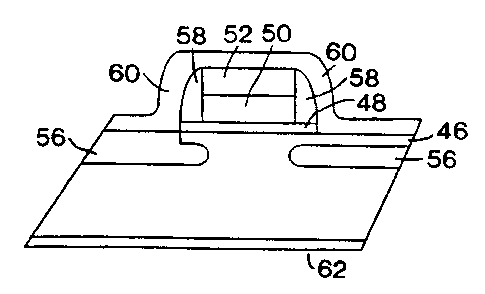
A process for fabricating a preferred embodiment of
the present invention is presented herein in reZation to
Figures 3a through 3v. Figure 3a illustrates a silicon
substrate 32 which, in Figure 3a and in some of the
subsequent Figures, is taken as a chip sized substrate,
though obviously numerous such chips are fabricated on a
single silicon wafer, as is well known in the
technology. In the specific embodiment described, the
substrate is an n-type substrate. -The first step is to
grow a thick silicon oxide layer 34 as shown in Figure
3b. Then, as shown in Figure 3c, a thin oxide layer 36
is deposited, and a layer of photoresist 40 is put down
and a window is defined therein within which the
ultimate circuit will be formed. Then using a wet etch
(Figure 3d), both the thin and thick oxide regions will
be etched. The thin oxide region, however, being a
deposited region, will etch much more rapidly than the
thick oxide region, allowing the etchant to undercut the
photoresist 40 to form an opening 42 through the thick
oxide having tapered sidewalls 44 thereon. Preferably,
the tapered sidewalls have an aspect ratio on the order
of 1 in 5 to 3. in 10. Thereafter, as shown in Figure
3e, the photoresist is removed and, if desired, the thin
oxide layer may also be removed. This defines a chip
region (Figure 3f) having an opening or window 42
through the thick oxide 34 to define the circuit area,
the chip area shown in Figure 3f of course being
replicated many times on the silicon wafer.
In Figure 3g, a thin oxide layer 48 is grown over
the substrate region defined by the window in the thick
oxide. This layer becomes the gate oxide, and
preferably has a thickness of approximately 250
Angstroms. Then as shown in Figure 3h, a thin n-type
layer 46 such as, by way of example, an arsenic layer,
is implanted through the gate oxide layer 48 throughout
= CA 02278308 1999-07-20
WO 98/33218 PCT/US98/00843
-10-
the substrate region defined by the window in the thick
oxide. Preferably this layer is only approximately 200
Angstroms deep in the substrate, and terminates adjacent
the lower (thin) edge of the tapered thick oxide because
of the shielding effect thereof. (This may be also seen
in Figure 3t, taken on an expanded scale in comparison
to Figure 3g.) Then, as shown in Figure 3i, a layer of
nitride 50 and a layer of polysilicon 52 is put down
thereover. The nitride layer 50 and the polysilicon
layer 52 are patterned to form a plurality of pedestals,
generally indicated by the numeral 54 in Figure 3j.
These pedestals may be any convenient shape, such as, by
way of example, circular, hexagonal, rectangular or
square. In that regard, in the embodiment being
described, the pedestals are approximately 1 micron
square and arranged in a two dimensional array, whereby
a typical circuit may have on the order of 1.2 million
such pedestals. An alternate embodiment, however, may
use rectangular pedestals of say approximately 1 micron
wide, but having a length of many microns, so that the
number of pedestals across one dimension of the circuit
are far fewer (as few as one) than the number of
pedestals across a second dimension of the circuit. In
any event, the pedestals are formed by putting down a
layer of photoresist, patterning the same, and then
plasma etching, so that the pedestals will have
substantially straight (vertical) sidewalls, as opposed
to somewhat tapered sidewalls typically provided by wet
etching.
Alternatively, the pedestals may be fabricated of
other materials, such as by way of example, depositing a
nitride, oxide, nitride sandwich of layers rather than
the polysilicon layer. The pedestals may be entirely
nonconductive, or alternatively, if they have a
conductive layer, should be insulated from the substrate
*
CA 02278308 1999-07-20
WO 98/33218 PCT/US98/00843
-11-
thereunder. Thus the thin oxide layer under the
pedestals of this embodiment may be considered part of
the pedestals themselves, separate and apart from the
thin oxide of the same layer extending over the region
between pedestals. For instance, an equivalent
structure may be fabricated by first forming the
pedestals by forming one or more layers on the
substrate, at least the first of which is a dielectric
(electric insulator) such as an oxide or a nitride, and
then etching the layer or layers as described to form
the substantially vertical walled pedestals, exposing
the substrate between pedestals. Then a thin oxide
layer could be grown in the region between pedestals.
Then, as shown in Figure 3k, a thin layer of
material 55 such polysilicon or an oxide is deposited,
preferably approximately 1000 Angstroms thick. Because
this is a deposited layer, the layer will have
approximately the same build-up on all surfaces, whether
horizontal or vertical. In a subsequent plasma etch,
however, the layer will be removed substantially
equally, but only in the vertical direction. Thus, a
subsequent plasma etch of 1000 Angstroms will remove the
layer from the horizontal surfaces but leave regions 55
on the sides of the pedestals, each approximately 1000
Angstroms thick, as may be seen in Figure 3n.
The next step, shown in Figure 31, is to implant p+
regions 56 through the thin oxide 48 and deep enough in
the silicon substrate 32 to not convert the n region 46
of Figure 3g to a p region, but to place a p+ region
immediately there below. Typically this p+ region will
be on the order of 2000 Angstroms thick, in the
preferred embodiment formed by the implantation of
boron. Because of this thickness (reflected in the
energy of the ion implant), part of the region under the
CA 02278308 1999-07-20
WO 98/33218 PCT/US98/00843
-12-
tapered thick oxide region (see Figure 3t) will also be
implanted, forming a longitudinally graded junction
between the p+ implanted region and the n-type
substrate. This graded junction is characterized by a
gentle curve of the resulting pn junction from the
already shallow junction to the substrate surface under
the tapered thick oxide 44, typically on the order of
one half way up the taper.
After the implant, the thin regions 55 are removed
by etching. To best accommodate the removal of thin
regions 55, it is convenient to use a different material
for regions 55 than was used for the pedestals so that a
selective etch may be used to remove all traces of the
thin regions 55 without effecting the pedestals.
Then, as shown in Figure 3m, a layer of polysilicon
58 is deposited, this time preferably approximately 0.5
microns thick. Again, because this is a deposited
layer, the polysilicon will have approximately the same
build-up on all surfaces, whether horizontal or
vertical. In a subsequent plasma etch, however, the
polysilicon will be removed substantially equally, but
only in the vertical direction. Thus, a subsequent
plasma etch of 0.5 microns will remove the polysilicon
from the horizontal surfaces but leave polysilicon
regions 58 on the sides of the pedestals, as may be seen
in Figure 3n.
Again, alternatively other materials may be used,
such as, by way of example, by putting down a layer of
silicide approximately 250 Angstroms thick followed by a
oxide approximately 250 Angstroms thick, instead of the
polysilicon (silicides are usually thinner and normally
would require a suitable spacer material such as
polysilicon or oxide to achieve the desired thickness).
CA 02278308 1999-07-20
WO 98/33218 PCT/US98/00843
-13-
At this stage of fabrication, the circuit appears
generally as shown in the schematic representation of
Figure 3o. As stated before, in this exemplary
embodiment, square pedestals are being used so that
within the window of the tapered thick oxide (see Figure
3e) there is a two dimensional array of a multitude of
substantially square pedestals. As previously
mentioned, alternatively the pedestals may have a
substantial length in one dimension though will be small
in the other dimension, being approximately 1 micron in
the smaller (or both) dimensions in the presently
preferred embodiments.
The next step in the fabrication, shown in Figure
3p, is to etch away the thin oxide everywhere except as
masked by the pedestals. As part of this etch, or as a
separate etch, the thick oxide 34 is given a controlled
etch to shift the end of the tapered region 44 (Figure
3t) back approximately half way to the pn junction at
the surface of the silicon substrate (Figure 3u). Also,
using a photo-resist mask, boron is implanted in a small
percentage of the total area of the circuit to convert
the corresponding part of the n-type region 46 to a p+
region 56 to allow electrical contact to the P+ region
thereunder as shown in Figure 3q. The purpose of
electrically connecting to the p+ region 56 in limited
areas is to provide an opportunity to determine the
voltage thereof, as otherwise the p+ region would be a
floating region. Since the pn junction between the p+
region and the surrounding n regions will always be back
biased, the p+ region 56 is not a current carrying
region, and accordingly the area of such contacts can be
purposely kept small in comparison to the area of
contact to be made to the n region 46 thereover over
most of the circuit. In that regard, note also that
while the Figures such as Figure 3p show the p+ regions
CA 02278308 1999-07-20
WO 98/33218 PCTIUS98/00843
-14-
56 separated from each other by the pedestals, the p+
regions are interconnected between pedestals as
suggested by Figure 3o, so that the p+ region 56 is a
single region perforated with an array of openings, one
at each pedestal.
Finally, one or more interconnect layers 60 are
deposited over the circuit in the window 42 on the
substrate (Figure 3f), as well as over the tapered
region 44 on the thick oxide (see Figure 3v). This
interconnect layer makes electrical contact with n
region 46 over most of the area of the circuit (Figure
3r) and in a small percentage of the circuit area, makes
electrical contact with the p+ diffused regions 56
(Figure 3s). The interconnect layer may be a single
layer or a plurality of layers such as polysilicon, a
silicide and/or metal layers. The interconnect layer
forms the anode of the resulting diode, interconnecting
the polysilicon gate region 58 (and nitride regions 50
and polysilicon regions 42) with drain regions 46
(Figure 3r) and p+ regions 56 (Figure 3s). The source
connection is made from the back of the substrate
through metallized layer 62 (Figures 3r and 3s).
Between drain regions 46 and source regions 64 are very
short channel regions 66, defined primarily by the
approximately 0.5 micron wide polysilicon region 58
during fabrication of the device.
By appropriate selection of dopants and their
concentrations, and other materials and dimensions of
the device, the channel regions may be made to be just
conducting at a zero forward bias. In such a case,
simulations have shown that forward biasing of the
device by applying a positive voltage to contact layer
60 with respect to contact layer 62 of something less
than two tenths of a volt will provide a forward current
. . . . .._.__.__.........~.T.~._.._....._.._........ . . ..
___..~......__..~.. _..._. _-. 7.. . . _......,..... _ . . . _ .
CA 02278308 1999-07-20
WO 98/33218 PCTIUS98/00843
-15-
of at least two orders of magnitude greater than the
reverse bias leakage current. The simulations also show
that a forward bias on the order of three tenths of a
volt provides a forward current flow of at least three
orders of magnitude greater than the reverse bias
leakage current. Thus, in true rectifying applications
such as in power supplies and the like, the present
invention will clearly result in reduced power
consumption and heating in the rectifying devices, and
greater overall efficiency of the resulting circuits.
With respect to the reverse bias breakdown voltage
of the resulting diode, the reverse bias voltage appears
between p+ region 56 and the n-type substrate 32 (see
Figure 3v). The shallow curvature of the p+ region 56
adjacent the edges thereof, resulting from the
longitudinally graded junction fabrication technique
herein before described, avoids concentration of the
field lines in that area. Similarly, the extension of
the upper interconnect layer 60 over the tapered regiot
44 of the thick oxide 34 in effect tends to continue the
lines of equipotential, without concentration, out of
the substrate into the silicon oxide. This is
illustrated in Figure 4, which is a reproduction of a
computer simulation of the field lines on both sides of
the pn junction and in the oxide when the device is
subjected to a reverse bias of 80 volts. While the
field lines tend to concentrate once in the silicon
oxide, the silicon oxide is characterized by a higher
breakdown voltage than the silicon substrate. In the
substrate, however, there is very little concentration
of the field lines, giving the device a reverse bias
breakdown voltage closely approaching the inherent
reverse bias breakdown voltage of the silicon substrate
itself. This effect is maximized by bringing the end of
the taper of the thick oxide 44 back approximately half
CA 02278308 1999-07-20
WO 98/33218 PCT/US98/00843
-16-
way to the pn junction formed between p+ region 56 and
the n-type substrate where the pn junction meets the
surface of the substrate. However an advantageous
effect can still be achieved with the graded junction of
the present invention by omitting the step of giving a
controlled etch of the thick oxide 34 to shift the end
of the tapered region 44 (Figure 3t) back toward the pn
junction at the surface of the silicon substrate (Figure
3u). This still substantially reduces the concentration
of field lines in the substrate over other known
techniques, both because of the better longitudinal
gradation of the junction, and the tapered spacing of
what amounts to a field plate over the tapered thick
oxide.
In the fabrication of the device just described, in
general four masks are used. The first is to pattern
the photoresist 40 (Figure 3c), which in effect defines
the location of the substrate window surrounded by the
tapered thick oxide. This alignment is of course not
critical. The second mask is the pedestal mask, which
defines the positions of the pedestals within the
window. Because of the spacing provided between the
outer pedestals and the tapered thick oxide, and the
absence of any other specific alignment requirements,
alignment of the pedestal mask with respect to the first
mask is also not critical. The third mask is a mask
defining the small percentage of the circuit area over
which the arsenic implant region will implanted with
boron to make electrical contact with the boron
implanted p+ region thereunder. Since it doesn't matter
where on the circuit this occurs, the positioning of
this mask with respect to either of the prior two masks
is also not critical. Finally, the mask which defines
the sheet serving as the interconnect layer also
simultaneously defines the integral field plate layer
~T- T
CA 02278308 1999-07-20
WO 98/33218 PCT/US98/00843
-17-
extending up over the tapered thick oxide. Here again,
this alignment is also not critical with respect to the
location of any of the three prior masks. Accordingly,
there are no critical mask alignment requirements with
respect to the fabrication technique herein before
described, so that relatively crude alignment may be
used in comparison to that generally required for the
processing of conventional devices.
In the foregoing description, the n-type layer 46
(Figure 3h) was implanted after the thin oxide layer 48
was grown. As an alternative, the n-type implant may be
done instead after the pedestals are formed (Figure 3j).
In this case, before the implant the pedestal regions
would appear as shown in Figure 3w, and after the
implant the pedestal regions would appear as shown in
Figure 3x. Obviously the Figures following Figure j
would be correspondingly changed also.
A further alternate method of fabrication for the
present invention may be seen in Figures 5a through 5c.
In Figure 5a, after the structure of Figure 3p has been
formed, a layer of titanium nitride (TiN) is deposited
and plasma etched to leave TiN side regions 70,
electrically connecting the side regions 58 forming the
gate regions to the substrate region 46. Then a further
boron implant is made to extend the p+ regions to the
surface of the substrate, as shown in Figure 5b.
Finally, a further conductive layer or layers are
deposited, such as Tin layer 72 and tungsten silicide
layer 74 shown in Figure 5c. In this process, the TiN
sidewall regions 70 provide good electrical conn-ection
of the gate regions 58 and the substrate, allowing the
use of the rest of the substrate area between pedestals
to be converted to P+. This eliminates one masking
step, namely that used to convert a small percentage of
CA 02278308 1999-07-20
WO 98/33218 PCT/US98/00843
-18-
the substrate area between pedestals (Figure 5p) to a p+
regions (Figure 3q). While that masking step is not
critical in alignment, its elimination is a
simplification of the process. In that regard, note
that, as an example, the boron implanting is over the
entire area without masking the pedestals, as any
implantation on the pedestal sidewalls or tops is of no
consequence.
In certain instances in the foregoing description,
certain alternate materials and methods were set forth.
It is to be noted however, that the identification of
specific alternative materials and processes is not to
infer that still other materials and processes for those
or other steps in the process of fabrication or in the
resulting diode devices are excluded from use in the
present invention. To the contrary, steps and materials
other than those set out herein will be obvious to those
skilled in the art. Thus while the present invention
has been disclosed and described with respect to certain
preferred embodiments, it will be understood to those
skilled in the art that the present invention diodes and
methods of fabricating the same may be varied without
departing from the spirit and scope of the invention.
_._.._.T__..,__