Note: Descriptions are shown in the official language in which they were submitted.
CA 02278346 1999-07-21
' . ..
Specification
IC Card
Technical Field
The present invention relates generally to IC cards, and more
particularly, to an IC card capable of displaying a response state in a data
communication.
Background of the Invention
There have been known IC cards used for a data communication with
an externally provided interrogator.
Fig. 6 is a schematic block diagram of the basic configuration of a
conventional IC card 300. The conventional IC card 300 as shown is a
signal superposing, non-contacting type IC card, supplies power and
transmits/receives information using a signals) having one or more
frequencies received from an interrogator which is not shown.
IC card 300 shown in Fig. 6, an example of an IC card using a single
frequency, includes a tuning circuit 15, a rectifying circuit 16, an
amplifying/demodulating circuit 17, a modulating/amplifying circuit 18,
and an SP/PS conversion circuit 19. .
Tuning circuit 15 includes a coil L functioning as an antenna and a
capacitor C. Rectifying circuit 16 rectifies a signal received at tuning
circuit 15 to generate electric power and supplies the power to each part of
IC card 300. Meanwhile, amplifying/demodulating circuit 17 amplifies
and demodulates information Q fiom an interrogator received at tuning
circuit 15. A signal output from amplifying/demodulating circuit 17 is SP-
converted by SP/Ps conversion circuit 19.
Referring to Fig. 6, this conventional IC card 300 includes a main
control circuit 11 and a memory 10.
Main control circuit 11 processes a signal output fiom SP/PS
conversion circuit 19. Data output from main control circuit 11 which is to
be held is stored (held) in memory 10 for holding data.
-1-
CA 02278346 1999-07-21
Main control circuit 11 reads out data from an addressed region of
memory 10 based on the content of information Q received from the
interrogator, and generates response information A based on the read out .
data. Response information A is PS-converted by SP/PS conversion circuit
19, then processed by modulating/amplifying circuit 18 and transmitted to
the interrogator through antenna L.
The response state of such conventional IC card 300 is verified
exclusively on the side of the interrogator which is not shown) in other
words) conventional IC card 300 does not have a function to verify the
response state.
Therefore) information on what is going on in IC card 300 is not
available to the side of the user of the card.
For example, if a plurality of IC cards 300 perform a data
communication simultaneously or sequentially without time interval, and a
response abnormality from any of IC cards 300 is detected on the side of
interrogator, the user cannot find which IC card 300 has the abnormality in
the data communication.
Thus, the reliability of the entire system including the interrogator
and the responding element (IC card) can be hardly secured.
It is therefore an object of the present invention to provide an IC card
permitting the user to recognize a response state in a data communication.
Another object of the invention is to provide an IC card capable of
continuously displaying a response state in a data communication for a
prescribed time period.
Disclosure of the Invention
An IC card according to the present invention performs a data
communication in response to externally applied data, and includes a
control circuit to control data reception and a response, and a display to
display a response state in response to an instruction from the control
circuit.
An IC card according to another aspect of the invention performs a
data communication in response to externally applied data, and includes a
-2-
CA 02278346 1999-07-21
storing circuit to which the externally applied data is written, a control
circuit to control a response using the data written in the storing circuit,
and a display to display a response state in response to an instruction from
the control circuit.
An IC card according to a further aspect of the invention performs a
data communication in response to externally applied data, and includes a
first storing circuit to which the externally received data is written, a
second storing circuit to save the written data in the first storing circuit)
a
control circuit to make control for making a response using data in the first
or second storing circuit, and a display circuit to display a response state
in
response to an instruction received from the control circuit.
Therefore, a main advantage of the present invention resides in that
the user may readily visually recognize a response state in a data
communication.
Brief Description of the Drawings
Fig. 1 is a block diagram of the configuration of a main part of an IC
card 100 according to a first embodiment of the present invention;
Figs. 2 and 3 give a flow chart for use in illustration of data holding
and data recovery operations and a response state display in IC card 100
according to the first embodiment;
Figs 4A to 4C are views each showing an overview of IC card 100
according to the first embodiment;
Fig. 5 is a block diagram of the configuration of a main part of an IC
card 200 according to a second embodiment of the present invention; and
Fig. 6 is a schematic block diagram of the configuration of a
conventional IC card 300.
Best Mode for Carrying Out the Invention
First Embodiment
An IC card according to a first embodiment of the invention has a
displaying function and can externally display the response state of the IC
card in a data communication based on the state of writing data in a
-3-
CA 02278346 1999-07-21
memory for holding data.
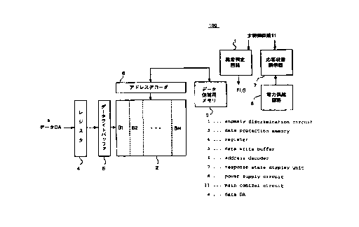
Fig. 1 is a block diagram of the configuration of a main part of IC
card 100 according to the first embodiment, and the remaining part is the
same to that of the conventional IC card 300 shown in Fig. 6 (except for
memory 10), and therefore the remaining part is not shown and described.
Note that the IC card to which the present invention is applied may be a
contacting type or non-contacting type IC card.
IC card 100 shown in Fig. 1 is different from IC card 300 as follows.
IC car d 100 includes a non-volatile memory for holding data 2 (hereinafter
data holding memory 2) and a non-volatile memory for protecting data 3
(hereinafter data protecting memory 3) in place of memory 10, an
abnormality determination circuit 1 to determine the state of writing data
in data holding memory 2) a response state display 7 to display a response
state, and a power supply circuit 8 to supply power to response state
display 7 for a prescribed time period.
Referring to Fig. 1, the configuration of IC card 100 according to the
first embodiment will be now described.
A register 4 receives data DA to be held, received in the present data
communication from main control circuit 11 shown in Fig. 6. Register 4
may be formed by an SRAM. A data write buffer 5 is a circuit to wizte
data in register 4 into data holding memory 2. An address decoder 6 is a
circuit to address a region of data holding memory 2 to/from which a data
writing/reading operation is performed.
Data holding memory 2 stores data DA received from register 4.
Referring to Fig. 1, data holding memory 2 according to the first
embodiment stores data DA received by a single data communication in any
of regions B1) B2, ..., BN under the control of main control circuit 11. A
non-volatile device such as flash memory is used for data holding memory 2.
IC card 100 according to the first embodiment performs a data
communication based on data stored in data holding memory 2. Therefore,
if there is an abnormality in data holding memory 2, an abnoi~nality occurs
in a data communication.
Data protecting memory 3 serves to save data stored in data holding
-4-
CA 02278346 1999-07-21
memory 2 and is used to recover the data in data holding memory 2 when
the data is destroyed. Referring to Fig. 1, data protecting memory 3
according to the first embodiment includes a capacity for storing data DA
received in a single data communication (not less than the capacity of
region B1, B2) ..., or BN). A non-volatile device such as flash memory is
used for data protecting memory 3.
Note that data to be written in data protecting memory 3 needs only
correspond to the content stored in data holding memory 2 on a one-to-one
basis) and the data may be the inverse of data in data holding memory 2.
Abnormality determination circuit 1 determines the state of writing
data in data holding memory 2 based on an instruction from main control
circuit 11, and records the result of determination in a state determination
flag FLG for output. For example, if there is an abnormality in the power
supply at the time of writing data, the data could be irregularly altered,
and therefore abnormality determination circuit 1 according to the first
embodiment determines the state of writing data in data holding memory 2
based on the state of the power supply to operate IC card 100.
As will be described, state determination flag FLG has its value
updated depending upon how data is processed. If data DA to be held in
data holding memory 2 is stored, state determination flag FLG is initialized.
(The state of writing data is determined normal.) Meanwhile, if an
abnormality occurs in the process of writing data DA in data holding
memory 2, state determination flag FLG is not initialized regardless of the
following processes, and the value at the occurrence of the abnormality is
held. (The state of v~nzting data is determined abnormal.)
Note that the value of state determination flag FLG is held until the
next data communication processing. State determination flag FLG may
be formed for example by a non-volatile memory.
Response state display 7 receives an instruction fiom main control
circuit 11 and displays information related to the response state of IC card
100. More specifically, the display indicates the following contents
accor ding to state determination flag FLG. First, if the state of writing
data into data holding memory 2 is normal) an indication that a normal
-5-
CA 02278346 1999-07-21
response has been completed (normal communication completion
indication) is given. Secondly, when the state of writing data into data
holding memory 2 is abnormal, but the data has been recovered using data
in data protecting memory 3) an indication that the data has been
recovered (data recovery indication) is given. Thirdly, when the state of
writing data in data holding memory 2 is abnormal and there is no recovery
data in data protecting memory 3, an indication that the response has been
abnormal (communication abnormality indication) is given.
Power supply circuit 8 supplies power to response state display 7 for
a prescribed time period. Response state display 7 receives the power
supplied from power supply circuit 8 and continuously displays the
response state for a prescribed time period. Power supply circuit 8 may be
for example a circuit formed of a large capacity capacitor receiving current
from rectifying circuit 16 shown in Fig. 6, or a circuit including a storage
cell or a solar cell.
The operation of IC card 100 according to the first embodiment will
be now described.
Figs. 2 and 3 are flow charts each for use in illustration of operations
related to data holding and recovery operations by IC card 100 according to
the first embodiment. Herein, state determination flag FLG takes 0 or 1,
and the value is initialized to 0 if the state of writing data is normal.
Referring to Figs. 2 and 3, the data holding and recovery operations
and display of a response state by IC card 100 will be now described.
In step S 1, the IC card is activated.
In step S2, state determination flag FLG is checked, and it is
determined if data has been normally written in data holding memory 2
(=0).
The case in which state determination flag FLG takes 0, in other
words when the state of writing data in data holding memory 2 is normal
will be described.
Note that, although not illustrated, in the process of steps S3 to S5
except for the period of writing to data holding memory 2, IC card 100
performs a data communication using data in data holding memory 2.
-6-
CA 02278346 1999-07-21
In step S3, data DA is input to register 4. Data in region B 1 in data
holding memory 2 is then read out and the read out data is saved (written)
in data protecting memory 3. In step S4) state determination flag FLG is
set to 1 (to the state in which data in region B 1 in data holding memory 2
has been saved in data protecting memory 3). In step S5, data DA written
in register 4 is written in region B1 in data holding memory 2.
After the processing of step S5 (in the state in which data DA has
been wiztten in data protecting memory 2), response state display 7 gives a
normal communication completion indication in step S6. Then in step S7,
state determination flag FLG is initialized (=0).
Subsequently, the case in which state determination flag FLG takes
1, in other words, when the state of writing data in data holding memory 2
is abnormal will be now described.
Note that, although not illustrated, the following process is executed
after IC card 100 starts to be activated and before accessing to data holding
memory 2 is initiated.
It is checked in step S8 if data necessary for recovering data in data
holding memory 2 is present in data protecting memory 3. If no such data
is present (such as in the first communication in which no data is present
in data protecting memory 3), a communication abnormality occurs, and
therefore response state display 7 gives a communication abnormality
indication in step 12.
Meanwhile, if there is data for recovery, response state display 7
gives a data recovery indication in step S9. In step S10, data which has
been saved in data protecting memory 3 is read out, and the data is written
in region B1 in data holding memory 2. As a result, the data causing a
communication abnormality is destroyed, and normal data is written
(recovered) in data holding memory 2. After the recovery process in step
S 10 is completed, state determination flag FLG is initialized (=0) in step
S 11. After a normal state is attained in step S 11, the process in steps S3
to S6 is performed.
Figs. 4A to 4C are views each showing an overview of IC card 100
according to the first embodiment. As shown in Fig. 4A, for example)
_7_
CA 02278346 1999-07-21
response state display 7 may be formed using an LED (L1, L2, and L3 in
Fig. 4A). For example) L1, L2, and L3 in Fig. 4A may correspond to the
normal communication indication, data recovery indication, and
communication abnormality indication, respectively. Alternatively, the
use of LEDs of two colors makes it easier for the user to visually recognize
the normal communication indication and the communication abnormality
indication.
The content of display is not limited to the above, and other
communication contents (L4, L5, L6, and L7 in Fig. 4B) may be indicated.
Alternatively) response state display 7 may be formed by an LCD or
by both an LCD (L8 in Fig. 4C) and an LED (L1) L2 in Fig. 4C).
As descizbed above, IC card 100 has a display function, may
determine the state of writing data in data holding memory 2, and use the
result of determination to externally display the response state of IC card
100 in a data communication.
Second Embodiment
An IC card according to a second embodiment of the invention
externally displays the response state of the IC card in a data
communication using a main memory or a sub memory for holding data.
According to the second embodiment, not only an abnormality in the
power supply but also change in data caused by externally imposed stress,
or static electricity may be detected.
Fig. 5 is a block diagram of the configuration of a main part of an IC
card 200 according to the second embodiment, and the remaining part is
the same as that of the conventional IC card 300 shown in Fig. 6 (except
memory 10) and therefore is not shown or described. The card to which
the invention is applied may be a contacting type or non-contacting type IC
card.
IC card 200 shown in Fig. 5 is different from the conventional IC
card 300 in the following points. IC card 200 includes a non-volatile main
memory for holding data 20 (hereinafter simply as main memory 20) and a
non-volatile sub memory for holding data 21 (hereinafter simply as sub
memory 21) in place of memory 10, detection circuits 22 and 23 for
-g_
CA 02278346 1999-07-21
detecting errors in main memory 20 and sub memory 21, respectively, a
response state display 30 for displaying a response state, and a power
supply circuit 8 for supplying power to response state display 30 for a
presciZbed time period.
Referring to Fig. 5, the configuration of IC card 200 according to the
second embodiment will be described.
Main memory 20 and sub memory 21 are connected to a main control
circuit 11 through selectors 28 and 29, respectively.
Sub memory 21 is used as a backup memory for main memory 20,
and data corresponding on a one-to-one basis to data in main memory 20 is
written in this sub memory. Note that the data written in sub memory 21
may be the inverse of data written in main memory 20, or data
complementary to the data written in main memory 20.
Main memory 20 and sub memory 21 may be formed by an EEPROM,
a flash memory, a ferroelectric memory or the like.
Error detection circuits 22 and 23 detect errors in data written in
main memory 20 and sub memory 21, respectively. Error detection
circuits 22 and 23 control selectors 28 and 29 based on the result of
detection. As a result, a memory (main memory 20 or sub memory 21)
which allows main control circuit 11 to read out data is selected.
Error detection circuits 22 and 23 may be a parity check circuit) a
CRC check circuit or the like. Errors may be detected on a one-bit-basis or
a multi-byte-basis.
Error correction circuits 26 and 27 correct errors detected by error
detection circuits 22 and 23) respectively.
Response state display 30 receives an instruction from main control
circuit 11 and gives an indication related to the response state of IC card
200. More specifically, the indication is switched depending upon the
error detection about main memory 20 and sub memory 21. Response
state display 30 may be formed by an LCD or LED as described in
conncetion with the first embodiment of the invention.
Power supply circuit 8 supplies power to response state display 30 for
a prescizbed time period as descubed in connection with the first
_g_
CA 02278346 1999-07-21
embodiment.
The operation of IC card 200 according to the second embodiment
will be now described.
When main control circuit 11 receives data from an interrogator,
main control circuit 11 has data DA stored in main memory 20 and sub
memory 21 through selectors 28 and 29, respectively.
Error detection circuit 22 detects the presence/absence of an error in
the data stored in main memory 20. If an error is not detected in the data
in main memory 20, error detection circuit 22 controls selector 28 such that
the data is to be read out to main control circuit 11 from main memory 20,
and controls selector 29 such that data is not to be read out fiom sub
memory 21. Meanwhile, if an error is detected in the data in main
memory 20, control circuit 11 controls selector 28 such that the data is not
to be read out fiom main memory 20 and controls selector 29 such that data
is to be read out from sub memory 21.
Error detection circuit 23 detects the presence/absence of an error in
the data stored in sub memory 21. If an eiTOr is detected in sub memory
21 as well as in main memory 20, data is not provided from main memory
and sub memory 21 to main control circuit 11. In this case, main
20 control circuit 11 requests the interrogator to re-transmit the data or
clearly indicates the presence of the error. If an error is detected, error
correction circuits 26 and 27 read out data from main memory 20 or sub
memory 21 and then correct the data.
Response state display 30 makes a normal communication
completion indication when data is read out fiom main memory 20 or sub
memory 21 and gives a communication abnormality indication when no
data is read out from any of memories 20 and 21.
Response state display 30 may give a normal communication
completion indication when data is read out from main memory 20, a
backup indication when data is read out from sub memory 21, and a
communication abnormality indication when no data is read out from any
of memories 20 and 21.
Note that errors in data only in main memory 20 may be detected by
-10-
CA 02278346 1999-07-21
error detection circuit 22 without providing error detection circuit 23. In
this case, response state display 30 needs only be adapted to give a normal
communication indication and a communication abnormality indication.
As descizbed above) IC card 200 having a display function may detect
errors in data in main memory 20 and sub memory 21 and may externally
display the response state of IC card 200 in a data communication based on
the result of detection.
As in the foregoing, an IC card according to the present invention
has a display function and may externally display a response state in a
data communication using the result of determination of the state of
writing data.
Furthermore, with the power supply function, the response state
may be continuously. displayed for a prescribed time period.
As a result, the reliability of the IC card may be improved.
-11-