Note: Descriptions are shown in the official language in which they were submitted.
CA 02278615 1999-07-23
WO 99/27538 PCT/US98/25003
-1-
Description
ZERO POWER HIGH SPEED CONFIGURATION MEMORY
TECHNICAL FIELD
The present invention relates to semiconductor
memory devices, and more particularly to serial
configuration memories.
BACKGROUND ART
. Serial configuration memories are devices used
to initialize programmable logic devices, such as field
programmable gate arrays (FPGAs). When a device such as
an FPGA powers up, each of its logic blocks must be
configured for a specific logic operation and its
programmable interconnects must be configured to provide
routing among the logic blocks to implement the intended
logic function. The configuration information takes the
form of a bitstream which feeds into the FPGA and is
stored in the device, where the bits define logic and
routing of the FPGA elements.
A serial configuration memory is the device
which contains the configuration bitstream. A serial
configuration memory consists of a memory array such as a
PROM (programmable read only memory) or EEPROM
(electrically erasable programmable read only memory), an
address counter, and supporting logic to provide
programming and reset control. The address counter is
tied to a clock input line and is incremented on each
rising or falling edge of a clock signal. The counter
output serves to address each bit of the memory array,
producing a bitstream which is serially output to an
FPGA.
Many of today~s personal electronic devices are
powered by an independent source, namely a battery, and
so there is always a concern for conserving power
wherever possible. The desire to minimize power
consumption pervades every aspect of the design of these
CA 02278615 1999-07-23
WO 99/27538 PCT/US98/25003
-2-
devices. FPGAs find use in many such devices, including
laptop computers, notepad computers, and cellular
telephones. Configuration memories, therefore, present
an opportunity where improvements can be made to minimize
power consumption.
An aspect of modern FPGAs is their ability to
be reconfigured in-system. Thus, the functionality of an
FPGA can be dynamically altered while the system is
running. This capability provides a high degree of
flexibility for the system to adapt its operation in
response to external conditions. For example, in an FPGA
configured as a digital filter, its filter parameters can
be altered simply by loading in a different set of filter
coefficients when the need to do so is detected.
However, reconfiguring an FPGA in real time requires the
ability to download a new configuration bitstream without
imposing a delay that would detrimentally impact system
functionality. Thus, high speed operation is another
area for improvement in configuration memory devices.
Prior art configuration memories output their
entire contents in the form of a bitstream beginning with
the first location of memory. In-system reconfiguration
of an FPGA, however, requires access to any one of a
number of configuration bitstreams that might be
contained in a configuration memory, each bitstream
having its own beginning address within the memory. It
is a desire, therefore, to provide a configuration memory
wherein an arbitrary beginning address can be specified.
More generally, it is desirous to have the capability of
arbitrarily addressing the memory device.
SUMMARY OF THE INVENTION
The configuration memory device of the present
invention comprises a memory array organized as N-bit
data, typically eight bit bytes or sixteen bit words. An
external clock signal feeds into a divide-by-N circuit to
provide a trigger to initiate a memory access and to
sense the contents of an accessed memory location. Sense
CA 02278615 1999-07-23
WO 99/27538 PCT/US98/25003
-3-
circuitry provides parallel sensing of the N bits of the
accessed memory location. In the preferred embodiment,
the sense circuitry comprises N sense amps, one for each
bit being sensed.
The sense circuitry is enabled when a memory
location is being accessed. The sense circuitry remains
enabled for the time it takes to decode a memory address
and to sense the N bits in the addressed memory location.
Since the sense circuitry operates on all N bits at once,
the sense time is based on the speed of one sense amp.
The sense circuitry includes a latch to hold the sensed
data during the period of time between which the sense
amps are disabled and the data is loaded into the data
register.
The sense circuitry is coupled to a data
register which receives the sensed bits. The bits are
then serially shifted out synchronously with an external
clock. In accordance with the invention, the sensed bits
are loaded into the data register as the last bit of a
previously stored datum is shifted out of the data
register. As a result, the first bit of the sensed datum
is ready to be shifted out on the next clock. Meanwhile,
the next memory location is accessed and its bits are
sensed. This results in the continuous output of a
stream of bits at a rate equal to the frequency of the
external clock. More importantly this approach decouples
the operation of the sense circuitry, which is usually
slower than the clock speed, from the operation of
generating the bitstream output.
The device further includes means for
pre-loading the data register with a first datum from
memory during the power up sequence. This initializes
the data register so that there is data to shift out
while the next datum is accessed and sensed. In the
preferred embodiment, a cache register is loaded with a
datum from memory during the power up cycle, and from
there the data is subsequently loaded into the data
register.
CA 02278615 1999-07-23
WO 99/27538 PCT/US98/25003
-4-
In a preferred embodiment of the invention, an
address counter is coupled to the divide-by-N circuit to
provide an address every Nth clock. The address counter
feeds into a decoder to gain access to the memory, thus
providing a sequential access of the memory. In a
variation of the preferred embodiment, a means for
initializing the address counter is included so that
reading of the memory array can begin anywhere in the
array. This feature permits reading out of bitstream
l0 beginning from any location in the memory array. In yet
another variation, the address counter is replaced with a
means for receiving externally provided addresses. This
enables an external device to produce a bitstream
composed of an arbitrary sequence of memory locations.
BRIEF DESCRIPTION OF THE DRAWINGS
Fig. 1 is a system block diagram of the memory
device in accordance with the invention.
Figs. 2A - 2C and 3 illustrate the data caching
scheme of the invention.
Fig. 4 is a block diagram showing the memory
array of the present invention.
Fig. 5 is a schematic of a sense amplifier in
accordance with the invention.
Fig. 6 is a timing diagram showing the
operation of the sense amp of the present invention.
Fig. 7 illustrates a delay circuit used in
conjunction with the sense amplifiers.
Fig. 8 is a timing diagram of the principal
signals which participate in the operation of the
invention.
BEST MODE OF CARRYING OUT THE INVENTION
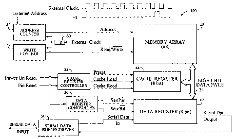
Referring to Fig. 1, a serial configuration
memory device 100 in accordance with the present
invention includes a memory array 20, typically organized
into an array of eight-bit bytes. Alternative data sizes
for the array can be used instead, e.g. sixteen-bit
CA 02278615 1999-07-23
WO 99/27538 PGT/LTS98/25003
-5-
words. In general, the present invention is capable of
operating with N-bit data sizes, where N preferably is a
power of 2.
An address counter 40 feeds into the memory
array 20 which includes a decoder for decoding the
address of a memory location. The address counter 40 is
clocked by the output of a divide-by-eight (=8) circuit
60. The =8 circuit is driven by an externally provided
clock signal to provide a pulse on every eighth cycle of
an EXTERNAL CLOCK. Fig. 1 shows a train of clock pulses
provided by the EXTERNAL CLOCK and the resulting pulses
produced by the =8 circuit. Thus, a stream of addresses
feeds into the memory array 20 at a rate of one address
every eighth clock. Again, in the general case the
circuit is a divide-by-N circuit for N-bit data sizes,
where an address is produced every Nth clock. A write
control module 32, also driven by the =8 circuit,
provides signaling to the memory array for read and write
operations. In addition, the write control module
signals a data register controller 36 to latch data read
out of array 20 into a data register 42.
The memory array 20 outputs the eight bits of
an accessed byte to data register 42 via a parallel
eight-bit data path 21. As mentioned above, data
register controller 36 operates the data register to
parallel load a byte (or an N-bit datum) read out from
memory 20 into data register 42; and to serially shift
its eight bits out of the SERIAL DATA OUTPUT line,
outputting the contents of memory 20 as a stream of bits.
The SERIAL DATA OUTPUT line feeds into a serial data
buffer 50 which drives the bitstream into an external
device, e.g. FPGA (not shown). The serial data buffer 50
also receives data to be written into the memory array 20
to effectuate programming of the configuration memory
device. Write control module 32 and data register
controller 36 together operate data register 42 to
serially shift data in from the SERIAL DATA INPUT and to
parallel write the shifted-in data into memory 20.
CA 02278615 1999-07-23
WO 99/Z7538 PCT/US98/25003
-6-
The configuration memory device of the present
invention further includes a cache register 44 coupled to
receive a byte of data during the power-up sequence, and
to load a byte previously stored in cache register 44
into data register 42 during a reset sequence. A cache
register controller 34 controls the cache register to
perform these operations, as will be explained below.
Referring now to Fig. 2A, data register 42 and
the cache register 44 comprise a series of one-bit stages
45. Each stage 45 includes a one-bit register 42n and a
one-bit cache latch 44n. Cache latch 44n receives its
input from an output of register 42n. A CACHE LOAD
control signal enables the cache latch to store the data
which appears at its input line. The output of the cache
latch feeds into an input of switch 43. Fig. 2B shows a
typical circuit for cache latch 44n, comprising a latch
circuit access which is gated by a transmission gate
controlled by the CACHE LOAD signal.
Register 42n receives input from switch 41 and
switch 43, and includes a PRESET control input. Switch
41 receives data from DATA LINE 21n and SERIAL DATA IN,
and is switched by the SER/PAR control line. The output
of switch 41 feeds into DATA IN of register 42n. Switch
43 receives data from cache latch 44n and from DATA LINE
21n, and is switched by the CACHE READ control line. The
output of switch 43 feeds into PRESET IN of register 42n.
Register 42n is clocked by the EXTERNAL CLOCK (not
shown). The output of register 42n feeds a SERIAL DATA
OUT line and as noted above feeds into cache latch 44n.
In addition, the output of the register 42n is fed back
to the DATA LINE 21n via pass transistor 48 which is
controlled by the WRT/RD control line.
The PRESET control input is driven by the
output of OR gate 46 which receives a PIN RESET signal
and a CACHE LOAD signal, both originating from cache
controller 34. PRESET control causes register 42n to
latch data in from the PRESET IN input rather than from
the DATA IN input. In addition to being latched into the
CA 02278615 1999-07-23
WO 99/27538 PCT/US98/Z5003
register 42n, PRESET control passes the PRESET IN input
directly to the output of the register. The reason for
this behavior will become apparent in the explanation
below. A typical circuit for the register 42n is shown
in Fig. 2C.
Data register 42 and cache register 44 (Fig. 1)
are comprised by the coupling together of eight of the
one-bit stages 45 in the manner shown in Fig. 3. For
example, data register 42 is built up by coupling the
SERIAL DATA OUT of one register 42n to the SERIAL DATA IN
of the subsequent register. The eight-bit data path 21
from memory array 20 (Fig. 1) comprises the DATA LINE 21n
of the stages 45. The SERIAL DATA OUTPUT (Fig. 1) of the
data register 42 derives from the SERIAL DATA OUT~line of
the stage holding the least significant bit, while the
SERIAL DATA INPUT of the data register is the SERIAL IN
of the stage containing the most significant bit. All of
the control lines are common to each of the stages.
Data register 42 and cache register 44 together
perform four fundamental tasks: the data register accepts
data in parallel fashion from an accessed memory
location; data stored in the data register is serially
shifted out on the SERIAL OUTPUT line; data to be stored
in memory array 20 is serially shifted in from the SERIAL
INPUT line; and data is presented in parallel fashion to
eight data-in buffers (not shown) in memory array 20 when
writing to a memory location.
Task 1: Loading data from an accessed memory
location involves a parallel read operation. This is
accomplished by asserting LO the WRT/RD and the SER/PAR
control lines of each of the one-bit stages 45 comprising
the data register 42. A LO on WR/RD turns off a pass
transistor 48, so that the output from memory 20 via DATA
LINE 21n feeds into switch 41 and 43. Also, a LO on
SER/PAR switches DATA LINE 21n to DATA IN of register
42n. The PIN RESET and CACHE LOAD lines are LO so that
the register clocks its data from DATA IN rather than
PRESET IN.
CA 02278615 1999-07-23
WO 99/27538 PCT/US98125003
_g_
Task 2: Serial shifting of data contained in
data register 42 is accomplished by asserting~a logic LO
on WRT/RD and a HI on SER/PAR. WRT/RD turns off pass
transistor 48 to isolate SERIAL DATA OUT from DATA LINE
21n. SER/PAR switches SERIAL DATA IN from a preceding
register 42n so that each tick of the EXTERNAL CLOCK
effectuates a shift propagation of the data from one
register 42n to the next.
Task 3: Serially shifted input from SERIAL
DATA INPUT (Fig. 1) requires asserting a HI on SER/PAR in
order to serially clock data into the data register.
WRT/RD is asserted LO to turn off pass transistor 48 so
that the output of register 42n is isolated from DATA
LINE 21n.
Task 4: Data shifted into the data register is
written into memory 20 by asserting a HI on WRT/R. Since
the data to be written is sitting at the output of each
register 42n, turning on pass transistor 48 presents the
data in parallel fashion to the data-in buffers (not
shown) of memory array 20.
During the power-up (power-on reset) sequence
and the externally driven reset sequence of the memory
device, operation of the data and cache registers 42, 44
proceed in a different manner. Referring again to Fig.
2, during a power-on reset (POR) cycle, CACHE READ is
asserted LO and CACHE LOAD is asserted HI. CACHE READ
switches DATA LINE 21n to PRESET IN of register 42n.
CACHE LOAD loads PRESET IN into register 42n. As
explained above with respect to Fig. 2C, asserting PRESET
couples PRESET IN directly to the output of the register
42n. Moreover, in the case when CACHE LOAD is asserted
HI, PRESET IN is loaded into the cache latch 44n as well
(see Fig. 2A and 2B). Thus, when a first byte of data
(usually the byte contained in memory location 0) is
sensed during the POR cycle, it is presented on the
eight-bit data path 21 (Fig. 1), which feeds into each
DATA LINE 21n, and is loaded into the registers 42n and
the cache latches 44n comprising data register 42 and
CA 02278615 1999-07-23
WO 99/27538 PCTlUS98/25003
-9-
cache register 44 respectively. This operation is
asynchronous, and when CACHE LOAD goes LO, data register
42 (as well as the cache register) contains the first
byte. When the first clock comes along, data register 42
will have been pre-loaded with a byte and will be ready
to start shifting data out.
During an externally driven reset cycle, there
is not enough time to sense and load the first byte into
the data register 42. Typically, a reset cycle completes
in a matter of tens of nanoseconds (e. g. 20 nanoseconds),
as compared to a POR cycle which requires on the order of
microseconds to complete before the device is ready to
output its bitstream. Recall, however, that the cache
register 44 has already been pre-loaded with the first
byte during the POR cycle. Thus, CACHE READ is asserted
HI so that PRESET IN is switched to receive the output of
the cache latch 44n. PIN RESET (via cache controller 34)
is asserted HI so that register 42n loads its input from
PRESET IN rather than DATA IN. Instead of accessing a
memory location and sensing the byte to be loaded into
the data register 42, the first byte is loaded directly
from the cache register 44 during a reset cycle, an
operation that can be accomplished within the time to
complete the reset cycle. Again, this is an asynchronous
operation, and as soon as the PIN RESET condition clears,
the data register 42 holds the cached byte and is ready
to be clocked out.
Referring now to Fig. 4, the memory array 20 is
shown comprising a cell array 20' having a plurality of
programmable memoxy cells, such as an array of floating
gate devices. X- and Y- decoders 60, 62 receive an
address and provide the necessary decoding logic to
access a memory location within cell array 20'. The
output of the Y-decoder feeds into sense amp circuitry 66
which comprises a series of eight sense amplifiers (Fig.
5) acting in parallel. In accordance with the present
invention, the Y-decoder feeds all N bits (e. g. 8 bits)
of an accessed memory location in parallel fashion into
CA 02278615 1999-07-23
WO 99/27538 PCT/US98/25003
-10-
the sense amp circuitry 66, thus providing parallel
sensing of the bits. The output of the sense circuitry
is coupled to the data register 42 via data lines 21. A
timer 64 provides an enable signal SAEN to turn on and
turn off the sense circuitry, and is driven by the=8
clock. SER/PAR latches the read out data from the sense
amps 66 into the data register 42.
Fig. 5 shows each such amplifier 200,
comprising sense amps 66, in greater detail. Transistors
T13 - T17 comprise a differential amp stage 230. On the
memory cell side of the diff. amp 230 is a voltage
reference section 210 and a current-to-voltage stage
comprising transistors T1 and T2. Similarly on the
reference cell side is a voltage reference 220 and a
current-to-voltage stage comprising transistors T7 arid
T8. The output 231 of the diff amp (i.e. the sensed bit)
feeds through pass transistor 256 to be stored in latch
250. The output of the latch is coupled to the sense amp
output line 21n via transmission gate 254 which is turned
on by the SER/PAR line.
The sense amp 200 further includes, in
accordance with the present invention, a sense amp
enabling circuit 270. The enabling circuit is driven by
a sense amp enable signal SAEN derived from the timer 64
shown in Fig. 4. The enabling circuit comprises a string
of inverters I1 - I4, interspersed with pairs of delay
capacitors C1/C2 and C3/C4. The output 271 of the
enabling circuit 270 operates a transmission gate
(comprised of transistor pair 252 and inverter I5) which
is coupled in-line with the latch 250 in the manner shown
in Fig. 5. The output 271 also drives (via inverter I5)
the gate of pass transistor 256.
With respect to the enabling circuit 270, the
SAEN signal feeds directly into input B of NAND gate G1
and into inverter I1. The output of inverter I1 feeds
into the gate of a P-channel transistor 246 and into
inverter 242. Inverter I1 turns on and off transistor
246 and inverter 242 at the same time. The output of
CA 02278615 1999-07-23
WO 99/27538 PCT/US98/25003
-11-
inverter I2 switches N-channel transistors T4 arid T10.
The output of inverter I4 feeds into input A of NAND gate
G1. Because of the delay capacitors, the signal arriving
at input A is delayed relative to the signal at input B
by an amount of time based upon the capacitance values of
the delay capacitors and to some degree the delay of
inverters I1 - I4.
Operation of the sense amp 200 will now be
described with reference to Fig. 5 and the timing chart
of Fig. 6. Referring first to Fig. 5, as SAEN
transitions from LO to HI during a power-up sequence, the
signal out of inverter I1 goes LO, thus turning on
transistor 246 thereby supplying V« to transistors T1,
T6, T7, and T12. Inverter I1 also turns on transistor
T17 via inverter 242, thus enabling differential amp 230
by providing a path to ground. A short delay thereafter,
the output of inverter I2 goes HI. This turns on
transistors T4 and T10, thereby turning on the voltage
reference stages 210, 220. At this time, the power-up
sequence for the sense amp has completed. This power-up
sequence guarantees a clean switchover of the sense amp
from a non-powered state to a powered state, avoiding any
transients which might appear at the sense amp output 21.
Turn now to the timing of the input signals at
inputs A and B of NAND gate G1 during power-up shown in
Fig. 6. Prior to time to, and for a period of time Ot
after ta, NAND gate G1 is HI since A and B are both LO.
Latch 250, therefore, is able to retain its state by
virtue of transmission gate 252 being on. At the same
time, latch 250 is isolated from the output 231 of diff.
amp, since pass transistor 256 is off. Because of the
delay capacitors C1 - C4, the signal at input A arrives
subsequent to the signal at input B and thus gate G1
remains HI until time t~, Ot units after SAEN goes HI.
At t~, gate G1 goes LO which turns off transmission gate
252, thus clearing the latch and disabling it. Also pass
transistor 256 is turned on, thus connecting the output
of diff. amp 230 to the latch. The delay path ensures
CA 02278615 1999-07-23
WO 99/27538 PCT/US98/25003
-12-
that the state of the latch (and hence the previously
sensed data) is retained until after the sense amp is
fully powered.
Continuing, consider when the sense amp begins
its power-down sequence as SAEN transitions from HI to
LO. Referring back to Fig. 5, the output of inverter I1
goes HI which turns off transistor 246, thus removing Vac
from transistors T1, T6, T7, and T12. In addition,
transistor T17 is turned off (via inverter 242), thus
disabling the diff. amp 230. The output of inverter I2
next goes LO which turns off transistors T4 and T10,
thereby shutting down the voltage reference stages 210,
220. At this time, the power-down sequence for the sense
amp has completed.
Referring to Fig. 6 at time t2, the signal at
the B input, being coupled directly to NAND gate G1,
follows SAEN without delay. This causes G1 to transition
HI as soon as SAEN goes LO. The diff. amp output 231 is
latched into latch 250 by virtue of the transmission gate
turning on. At the same time, pass transistor 256 is
turned off so that the latch 250 is isolated from the
rest of the sense amp circuitry as it is being powered
down as described above. Thus, the sensed data is saved
before power-down of the sense amp is complete. In
addition, by de-coupling the sense amp output 231 from
the latch, any transients which might occur during the
power-down sequence will not corrupt the state of the
latch.
Refer now to Fig. 7 for additional detail of
the timing circuit 64 shown in Fig. 4. The SAEN signal
originates as the output of NOR gate 303 from the circuit
shown in Fig. 7. NAND gate 301 enables the timing
circuit when enabling signal EN goes HI. An incoming ~8
clock signal received at NAND gate 301 is delayed by a
decoder delay circuit 302 for a time ate. Decoder delay
302 provides a time delay sufficient to allow
incrementing the address register 40 (Fig. 1) and for the
address decoders 60, 62 (Fig. 4) to access a memory
CA 02278615 1999-07-23
WO 99/27538 PCT/US98/25003
-13-
location, prior to actually enabling the sense amplifiers
200. An inverter chain 306 ensures a minimum delay to
allow for incrementing and decoding the next address, by
delaying the biasing of pass transistor 310, in a
situation where the pulse width of the =8 clock is too
short.
After a delay Ote, the =8 clock causes the
output (SAEN) of NOR gate 303 to go HI, thus turning on
the sense amps 200. A sense delay circuit 304 delays the
=8 clock to ensure that the SAEN pulse remains asserted
for a period of time its sufficient for the sense amps to
sense the state of a memory cell.
The relative timing between the =8 clock and
the SAEN pulses are shown in Fig. 7. At time to, the
clock arrives and is delayed by circuit 302 for a period
of time Ot~. At time t~, SAEN goes HI for a period of
time Ots, enabling the sense amps 200. At time t2 SAEN
goes LO, thus turning off the sense amps.
Operation of the serial configuration memory
will now be discussed with reference to the timing chart
of Fig. 8. As indicated in the chart, an address is
produced every eighth clock (via the -s-8 clock 60, Fig.
1). Thus at a certain clock (call it clock 1), an
address transition begins. As explained above, shortly
after clock 1 (Ote, Fig. 7) SAEN is asserted HI via timer
64 to turn on the sense amp circuitry 66. SAEN is HI for
a period of time (its, Fig. 7) long enough to allow the
eight bits of the addressed memory location to be sensed.
SAEN then goes LO and the eight sensed bits are retained
internally in the sense amp latches 250, the retained
data being represented in Fig. 8 as INT DATA.
Meanwhile, data bits from a previously read out
memory location D~_~ are being shifted out of data
register 42, indicated in Fig. 8 as EXT DATA. In fact at
clock 0, bit one of D~_~ is being shifted out. Observe
that for most of the time that data is being shifted out
of data register 42, SER/PAR is HI, recalling from Figs.
CA 02278615 1999-07-23
WO 99/27538 PCT/US98/25003
-14-
2A and 3 that this effectuates a right shift of the
stored bits with each clock.
For clocks 1 - 7, bits 2 - 8 of D~_~ are shifted
out of the data register. At clack 7, bit 8 of D~_~ is
shifted out. Also at clock 7 SER/PAR is asserted LO for
a period of time extending into clock 8. Referring once
again to Figs. 2A and 3, a LO on SER/PAR causes switch 41
to load the sensed data from the DATA LINES 21n into the
register latches 42n. In the case shown in Fig. 8 at
clock 8, the data is D~. Thus when clock 8 comes around,
the next bit that is shifted out of the data register is
the first bit of D~, the memory location that was read out
during clocks 1 - 7 (while D~_~ was being shifted out) and
stored in latches 250 of the sense amps 200.
During clocks 1' - 7', the bits comprising D~
are shifted out of the data register. As the timing
chart shows, the process repeats. The next address A~+~
is presented at clock 1', the sense amps are turned on to
read out the eight bits of D~~, and latched into latches
250 just prior to turning off the sense amps. The D~~
bits remain in latches 250 until clock 7', at which time
bit 8 of D~ is shifted out and the D~~ bits are loaded
into the data register (via SER/PAR being asserted LO),
so that at clock 8', the next bit shifted out of data
register 42 is the first bit of D~,,~.
A few points worth noting: First, each of the
eight sense amps 200 is turned on every eighth clock, and
remains on only for a period of time sufficient to allow
for decoding an address and for sensing a bit. As the
timing chart illustrates, this permits the sense amps to
be turned off most of the time during the eight clocks
required to shift out a previously read-out byte. This
greatly reduces the steady state current drawn by the
sense amps, representing a significant reduction in power
consumption.
Second, the resulting bitstream output is
synchronous with the external clock. More importantly,
the output rate of the bitstream is independent of the
CA 02278615 1999-07-23
WO 99/27538 PCT/US98/25003
-15-
speed of operation of the sense amps. This is due to the
pipeline processing technique used in the present
invention. As the timing chart shows, the memory
location being read out at any one time is always one
location ahead of the memory location whose bits are
being output. A memory location is always being
'pre-fetched' while a previously 'fetched' location is
being output. This overlapping of the read out operation
and the bitstream output operation de-couples the
bitstream rate from the speed of the sense amps. Thus,
the rate of the bitstream is no longer limited by the
speed of the sense amp, as in prior art designs. Rather,
the bit rate is a function only of the external clock
frequency.
Third, this architecture is easily scaled up
for data sizes larger than eight-bit data. For example,
a sixteen-bit data path can be accommodated simply by
providing additional sense amps. The relative timing
would remain unchanged from that shown in Fig. 8. Thus,
for higher clock frequencies, where conceivably the sense
time might approach the time it takes to serially output
eight bits, extending the data size to sixteen bits would
provide a wider window of time during which data can be
sensed.
Fig. 1 also shows a variation of the embodiment
of the present invention. In this variation, the address
counter 40 includes an input shown in phantom far
receiving an initial address from an external source.
This allows pre-setting the address counter to a memory
location other than memory location zero so that the
bitstream can begin from anywhere in the memory array 20.
This is useful with reconfigurable FPGAs, where multiple
configuration bitstreams may be stored in the configura-
tion memory so that any one configuration can be sent to
the FPGA at runtime.