Note: Descriptions are shown in the official language in which they were submitted.
CA 02278708 1999-07-21
WO 98135237 PCTIUS98I01266
ARCING FAULT DETECTION SYSTEM
FIELD OF THE INVENTION
The present invention relates generally to arcing fault detection systems for
protecting an electrical distribution system from arcing faults. More
particularly, the
present invention relates to an apparatus and method for testing an arcing
fault detection
system.
BACKGROUND OF THE INVENTION
Electrical systems in residential, commercial and industrial applications
usually
include a panelboard for receiving electrical power from a utility source. The
power is
connected to the panelboard via line bus bars and neutral bus bars. The
electrical power is
delivered from the panelboard to designated branch circuits through line and
neutral
conductors supplying one or more loads. Typically, various types of protective
devices are
mounted to the bus bars of the panelboard to protect the branch circuits from
hazardous
electrical conditions and reduce the risk of injury, damage or fires.
Circuit breakers are a well known type of protective device which are designed
to
I S trip open and interrupt an electric circuit in response to detecting
overloads and short
circuits. Overload protection is provided by a thermal element which, when
heated by the
increased current, will cause the circuit breaker to trip and interrupt the
power. This can
occur when too many loads draw power from the same branch circuit at the same
time, or
when a single load draws more power than the branch circuit is designed to
carry. Short
circuit protection is provided by an electromagnetic element that trips when
sensing high
current flow. Circuit breakers may also provide protection against ground
faults which
occur when current flows from a hot conductor to ground through a person or
object.
Arcing faults, which occur when electric current "arcs" or flows through
ionized
gas between two ends of a broken conductor, between two conductors supplying a
load, or
between a conductor and ground, comprise one type of electrical hazard that
can not
generally be detected by standard circuit breakers. This is because current
levels associated
with arcing faults are generally not high enough to trip the thermal or
electromagnetic
elements associated with standard circuit breakers. Arcing faults typically
result from
corroded, worn or aged wiring or insulation, loose connections, wiring damaged
by nails or
staples through the insulation, and electrical stress caused by repeated
overloading,
SUBSTITUTE SHEET (RULE 26)
CA 02278708 2003-10-03
WO 98/35237 ~ " PCTIUS98101266
2
lightning strikes, etc. The presence of an arcing fault creates a significant
fire hazard
because it generates heat which may ignite the conductor insulation and
adjacent
combustible materials.
Arcing fault detection systems known in the art generally sense the current
passing
through the line conductor of a branch circuit, process the sensed information
to determine
whether the characteristics of the line current represent the occurrence of an
arcing fault,
and trip open the branch circuit if an arcing fault has occurred. A preferred
arcing fault
detection system of this type is described in United States Patent 5,682,101,
entitled
"Arcing Fault Detection System", issued October 28,1997, and assigned to the
assignee
of the present invention. The arcing fault detection system may sense line
voltage rather
than line current.
SUMMARY OF THE INVENTION
In accordance with one aspect of the present invention, there is provided a
system
for testing an arcing fault detection system in an electrical distribution
network having a
Line conductor carrying an electrical signal between a power source and a
load, the arcing
fault detection system including a sensor coupled to the line conductor for
monitoring the
electrical signal and generating a sensor signal representing the electrical
signal, the
arcing fault detection system generating an arc-indicative signal in response
to the sensor
signal having characteristics indicative of an arcing fault. The testing
system couples the
sensor to a test line simultaneously with the line conductor and periodically
produces a
test signal on the test line. The sensor simultaneously monitors the test
signal and the
_ electrical signal and produces a sensor signal representing both the test
signal and the
electrical signal when the test signal is present on the test line. The arcing
fault detection
system generates an arc-indicative signal in response to the sensor signal
associated with
either the test line or line conductor having characteristics indicative of an
arcing fault.
A diagnostic test integrator evaluates the status conditions of the test
signal and the arc-
indicative signal and generates a trip signal to trigger the interruption of
the electrical
signal in response to certain status conditions of the test signal and the arc-
indicative
signal.
In accordance with another aspect of the present invention, there is provided
a
system for detecting arcing faults in an electrical distribution system
including a plurality
CA 02278708 1999-07-21
WO 98/35237 PCT/US98/01266
3
of phase lines for connecting a power source to a respective plurality of
loads, and a
current transformer electrically coupled to one of the phase lines. The
current
transformer has a secondary Iine extending therefrom carrying an electrical
current. The
system monitors the secondary line for the occurrence of an arcing fault in
the
corresponding phase line and disconnects the load from the power source in
response to
the detection of an arcing fault in the corresponding phase line. The
monitoring of the
secondary line for the occurrence of an arcing fault comprises monitoring
changes in
current (or voltage) associated with the secondary line and producing a rate-
of-change
signal representing the rate of change of current (or voltage) associated with
the
to secondary line. An arc-fault-detection signal is generated in response to
variations in the
rate-of change signal representing an arcing fault.
In accordance with another aspect of the present invention, there is provided
an
integrated protection system for an electrical distribution system including a
panelboard
for receiving and distributing power from a utility source. The panelboard
receives
power from the utility source through at least one line bus and a neutral bus.
The
panelboard distributes power to a plurality of branch circuits each having
line and neutral
conductors for delivering the power to a load. The line conductors are
electrically
connected to one of the line buses and the neutral conductors are electrically
connected to
the neutral bus. The panelboard includes a framework having a plurality of
positions for
attaching circuit protection devices to the plurality of branch circuits. The
integrated
protection system comprises a plurality of arcing fault detector modules and
line
interrupters, each attached to one of the positions in the panelboard
framework. The
arcing fault detector modules are adapted to detect the occurrence of an
arcing fault in
either of the selected number of branch circuits, while the line intemzpters
are adapted to
disconnect the load from the power source in response to the detection of an
arcing fault
in one of the selected branch circuits. An isolation module attached to one of
the
positions in the panelboard may be provided for electrically isolating arcing
fault signals
to the branch circuit in which they occur.
In accordance with another aspect of the present invention, there is provided
an
3o integrated protection system for an electrical distribution system
substantially as
described above, comprising a plurality of combination arcing fault detector
and line
CA 02278708 1999-07-21
WO 98135237 PCTIUS98/01266
4
internzpter modules, each associated with one of the branch circuits and
attached to one
of the positions in the panelboard framework. An arcing fault detector portion
of the
module is designed to detecting the occurrence of an arcing fault in its
respective branch
circuit, while a line interrupter portion of the module is designed to
disconnect the load
from the power source in response to the occurrence of an arcing fault in the
respective
branch circuit. An isolation module attached to one of the positions in the
panelboard
may be provided for electrically isolating an arcing fault signal to the
branch circuit on
which it occurred.
In accordance with still another aspect of the present invention, there is
provided
an integrated protection system for an electrical distribution system
substantially as
described above, comprising a plurality of arcing fault detector modules and
line
internlpter modules. The line interrupter modules are each attached to one of
the
positions in the panelboard framework, while the arcing fault detector modules
are
attached externally to the line interrupter modules. The arcing fault detector
modules are
designed to detect the occurrence of an arcing fault in either of the branch
circuits, while
the line interrupter modules are designed to disconnect the load from the
power source in
response to the detection of an arcing fault in one of the branch circuits. An
isolation
module attached to one of the positions in the panelboard may be provided for
electrically isolating arcing fault signals to the branch circuit on which
they occurred.
In accordance with a further aspect of the present invention, there is
provided a
trip indicator for use in an electrical distribution system including a
plurality of branch
circuits each of which has line and neutral conductors for connecting a power
source to a
load. Each of the plurality of branch circuits includes an arcing fault
detector disposed
within a housing for detecting the occurrence of an arcing fault condition and
activating a
trip signal in response thereto and a line interrupter for disconnecting the
load from the
power source in response to the activation of the trip signal. The trip
indicator comprises
a light source adapted to illuminate in response to the activation of the trip
signal. A
conduit is provided within the housing for conveying light between the light
source and
an opening of the housing in response to illumination of the light source.
In accordance with another aspect of the present invention, there is provided
a trip
indicator for use in an electrical distribution system substantially as
described above, in
CA 02278708 1999-07-21
WO 98135237 PCTIUS98/01266
which the trip indicator comprises a plunger having a colored tip. The plunger
is
movable between a retracted position and an extended position in response to
the
activation of the trip signal. A conduit is provided within the housing for
conveying light
external to the housing toward the colored tip to produce a reflection of
colored light.
The conduit thereafter conveys the reflection of colored light to the opening
of the
housing.
In accordance with yet another aspect of the present invention, there is
provided a
trip indicator for use in an electrical distribution system substantially as
described above,
in which the trip indicator comprises a bimetal disk having a colored top. The
bimetal
l0 disk is thermally movable between a generally flat position and a convex
position in
response to the activation of the trip signal. A conduit is provided within
the housing for
conveying Iight external to the housing toward the colored top to produce a
reflection of
colored light. The conduit thereafter conveys the reflection of colored light
to the
opening of the housing.
In accordance with still another aspect of the present invention, there is
provided
a trip indicator for use in an electrical distribution system substantially as
described
above, in which each of the plurality of branch circuits includes two or more
protective
devices. Each of the protective devices is adapted to detect the occurrence of
respective
fault conditions and activate a trip signal in response thereto. The trip
indicator is
2o responsive to the activation of the trip signal and indicates which of the
respective
protective devices activated the trip signal.
In accordance with a further aspect of the present invention, there is
provided a
circuit breaker for interrupting the electrical current flowing through a line
conductor to a
load terminal in response to the detection of an arcing fault, ground fault
and/or overload.
The circuit breaker has a sensor for sensing the electrical current in an
electrical power
distribution circuit and for sending a signal representing the characteristics
of the current
to an electronic detector. When the detector detects the occurence of an
overload, ground
fault or arcing fault, a trip signal is sent to an actuator. In response to
the trip signal, the
actuator actuates a trip mechanism for opening and closing a pair of breaker
contacts
which open and close the electrical circuit.
CA 02278708 1999-07-21
WO 98!35237 PCT/LTS98I01266
6
In accordance with another aspect of the present invention, there is provided
an
isolation device for use in an electrical distribution network, the network
having a
plurality of branch circuits defined by line and neutral conductors connected
between a
power source and load, the line and neutral conductors being electrically
connected to
respective line and neutral buses in an electrical distribution panelboard,
the isolation
device comprising filter means for providing a low impedance path for an
arcing fault
signal occurring in a selected one of the branch circuits, the filter means
being coupled
between the line and neutral buses in the electrical distribution network.
A further aspect of the present invention facilitates automated production (or
hand assembly) of circuit breakers which include arcing fault detectors. Such
detectors
comprise a toroidal sensor having an annular core encompassing a current-
carrying load
line in which the sensing coil is wound helically on the core such as has been
described
in the patent applications referenced above. In one embodiment, the assembly
includes a
circuit board and a two-piece sensor core in a two piece housing. The lower
sections of
I5 the core and housing are connected to the circuit board and the upper
sections of the core
and housing are detachably mountable to their respective lower sections. A
helical
winding is placed on the lower core and is attached to conductive pins which
make
electrical contact with the circuit board. When the upper core is locked to
the lower core,
they form a hollow center oriented horizontally. Electrical power is supplied
to an
electrical load via attachment to a load line terminal located on one side of
the sensing
coil. The load line terminal extends through the hollow center of the sensing
coil. An
insulator is disposed around the portion of the load line terminal within the
center of the
sensing coil. A connection to the electrical supply is provided via a load
terminal which
is connected to the load line terminal after it has emerged on the opposite
side of the
sensing coil. In an alternative embodiment, the upper section of the housing
is omitted.
In another embodiment, the sensing coil is positioned on the circuit board so
that the
hollow center of the coil is oriented vertically and the load line terminal is
connected to
the load terminal above the sensing coil. Alternatively, the sensing coil may
be one-
piece and positioned with the hollow center mounted horizontally. In such an
embodiment, the ternunal would be inserted within the sensing coil and weld
connections
made to the load terminal and the circuit board after the sensing coil has
been positioned.
CA 02278708 1999-07-21
WO 98/35237 PCT/US9810I266
7
In accordance with yet another aspect of the present invention, there is
provided a
method and apparatus for detecting arcing faults in a line conductor carrying
an electrical
current between a power source and a load, the electrical current defining an
AC
waveform comprising a series of alternating positive half cycles and negative
half cycles.
The method comprises the steps of obtaining current samples in a series of
half cycles of
the waveform, determining the peak current of each of the half cycles, and
comparing the
peak currents to determine changes in slope between half cycles. The number of
changes
in slope occurring within a selected time interval are counted and an arc
indicative signal
is produced when the number of reversals in polarity of the slope occurring
within the
selected time interval equals or exceeds a predetermined threshold number.
In accordance another aspect of the present invention, there is provided an
alternative method and apparatus for detecting arcing faults in a line
conductor carrying
an electrical current between a power source and a load, the electrical
current defining an
AC waveform comprising a series of alternating positive half cycles and
negative half
cycles. The method comprises the steps of obtaining current samples in a
series of half
cycles, determining the peak current in each of the half cycles, and comparing
the peak
currents to determine slope changes between consecutive half cycles as
described above.
The method further comprises the steps of normalizing each of the current
samples and
autocorrelating the normalized current samples to obtain a measure of
significant
2o waveform shape changes between consecutive half cycles. Both the number of
changes
in slope and the number of significant waveform shape changes occurring within
a
selected time interval are counted and an arc indicative signal is produced
when the
number of reversals in polarity or the number of waveform changes equal or
exceed
predetermined threshold values.
BRIEF DESCRIPTION OF THE DRAWINGS
In the drawings, which comprise a portion of this disclosure:
FIG. 1 is a block diagram of an arcing fault detection system having a sensor
connected to the line conductor of a branch circuit;
FIG. 2 is a schematic diagram of an electrical circuit for implementing the
arcing
fault detection system illustrated in FIG. l;
FIGS. 3a through 3g are waveforms at various points in the circuit of FIG. 2;
CA 02278708 1999-07-21
WO 98135237 PCT/US98101266
8
FIG. 4 is a schematic diagram of an alternative circuit for use in place of
the
comparator and single-shot pulse generator in the circuit of FIG. 2;
FIG. 5 is a schematic diagram of an alternative circuit for implementing the
arcing fault detection system illustrated in FIG. 1;
S FIG. 6 is a schematic diagram of a test circuit which may be utilized in an
arcing
fault detection system according to principles of the present invention;
FIG. 7 is a schematic diagram of an alternative test circuit which may be
utilized
in an arcing fault detection system according to principles of the present
invention;
FIG. 8 is a flow chart of an arcing fault detection system and test method
according to one embodiment of the present invention;
FIG. 9 is a block diagram of an arcing fault detection system connected to
secondary lines of a current transformer according to principles of the
present invention;
FIG. 10 is a block diagram of a panelboard including an integrated protection
system according to one embodiment of the present invention;
IS FIG. 11 is a perspective view of a panelboard including the integrated
protection
system of FIG. 10 with an isolation module at the distribution panel;
FIG. 12 is a block diagram of a panelboard including an integrated protection
system according to another embodiment of the present invention;
FIG. 13 is a perspective view of a panelboard including the integrated
protection
system of FIG. 12 with an isolation module at the distribution panel;
FIG. 14 is a block diagram of a panelboard including an integrated protection
system according to still another embodiment of the present invention;
FIG. 15 is a perspective view of a panelboard including the integrated
protection
system of FIG. 14 with an isolation module at the distribution panel;
FIG. 16 is a perspective view of an isolation module which may be used in the
integrated protection systems of FIGs. 9-15;
FIG. 17 is a schematic diagram of an electrical circuit for implementing the
isolation module illustrated in FIG. 16;
FIG. 18 is a perspective view of an arcing fault detector module which may be
used in the integrated protection systems of FIG. 10 and 11;
FIG. 19 is a block diagram of the arcing fault detector module of FIG. 18;
CA 02278708 1999-07-21
WO 98/35237 PCTlUS98101266
9
FIG. 20 is a perspective view of a miniature circuit breaker housing which may
be
mounted to a panelboard and which may include the arcing fault detection
system of FIG.
1;
FIG. 21 is a top view of a miniature circuit breaker installed within the
miniature
circuit breaker housing of FIG. 20 in a closed (on) position and including a
trip indicator
according to one embodiment of the present invention;
FIG. 22 is a top view of a portion of the miniature circuit breaker of FIG. 21
in an
open (offltripped) position;
FIG. 23 is a side elevation of a trip indicator which may be positioned within
the
miniature circuit breaker housing of FIG. 20;
FIG. 24 is a top view of the miniature circuit breaker of FIG. 21 including a
trip
indicator according to another embodiment of the present invention;
FIG. 25 is a side elevation of a trip indicator which may be positioned within
the
miniature circuit breaker housing of FIG. 20 according to still another
embodiment of the
presentinvention;
FIG. 26 is a schematic diagram of an electrical circuit for implementing a
dual-
LED trip indicator according to one embodiment of the present invention;
FIG. 27 is a side elevation of a trip indicator which may be positioned within
the
miniature circuit breaker housing of FIG. 20 according to yet another
embodiment of the
presentinvention;
FIG. 28 is a side elevation of a trip indicator which may be positioned within
the
miniature circuit breaker housing of FIG. 20 according to still yet another
embodiment of
the present invention;
FIG. 29 is a side elevation of an alternative embodiment of the trip indicator
of
FIG. 26 including a push-to-reset and push-to-test feature;
FIG. 30 is a side elevation of an alternative embodiment of the trip indicator
of
FIG. 28 including a push-to-reset and a push-to-test feature;
FIG. 31 is a top view of the miniature circuit breaker of FIG. 21 including a
push-
to-test feature;
FIG. 32 is a side elevation of an alternative embodiment of the trip indicator
of
FIG. 27 including a push-to-reset and twist-to-test feature;
CA 02278708 1999-07-21
WO 98/35237 PCT/US98/OI266
FIG. 33 is a side elevation of a latching mechanism according to one
embodiment
of the present invention and illustrates the associated sensing and detection
circuits in
block diagram;
FIG. 34 is a plan view of a latching mechanism according to another embodiment
5 of the present invention;
FIG. 35a is a perspective view of a plunger/latch plate assembly for a
latching
mechanism according to another embodiment of the present invention;
FIG. 35b is a plan view of the plunger/latch plate assembly of FIG. 35a in
which
the latch plate has a rounded end;
10 FIG. 35c is a plan view of the plunger/latch plate assembly of FIG. 35a in
which
the latch plate has a L-shaped end;
FIG. 36a is a plan view of a latching mechanism comprising a latch plate with
an
integrated spring, coil and plunger according to another embodiment of the
present
invention;
FIG. 36b is a plan view of a latching mechanism comprising a latch plate with
an
integrated spring, coil and plunger according to another embodiment of the
present
invention;
FIG. 36c is a plan view of the latching mechanism of FIG. 36b with the
integrated
spring flexed;
FIG. 37 is a plan view of an electronically controlled circuit breaker with
integrated latch tripping including a high magnetic tripping conductor loop
according to
another embodiment of the present invention;
FIG. 38 is a plan view of an electronically controlled circuit breaker with
integrated latch tripping comprising a trip coil, armature and yoke according
to another
embodiment of the present invention;
FIG. 39 is a block diagram of an electrical distribution network using an
isolation
device according to principles of the present invention;
FIG. 40 is a perspective view of a panelboard which uses an isolation device
according to principles of the present invention;
FIG. 41 is a perspective view of an alternate isolation device according to
principles of the present invention;
CA 02278708 1999-07-21
WO 98/35237 PCT/US98/01266
11
FIG. 42 is a circuit diagram of the isolation device according to principles
of the
present invention;
FIG. 43 is a plan view of a circuit breaker incorporating an arcing fault
sensor
packaged within the miniature circuit breaker housing of FIG. 20;
FIG. 44 is a perspective view of a sensing coil connected to an internal load
connector and a load line terminal;
FIG. 45 is a partial perspective view of an alternate embodiment of the power
connection to the circuit board;
FIG. 46 is a partial perspective view of an alternative embodiment of the
lower
1 o housing;
FIG. 47 is a perspective view of the housing and sensing coil;
FIG. 48 is a partial perspective view of an alternative connection between the
internal load connector and load line terminal;
FIG. 49 is a perspective view of an alternative embodiment of the sensing coil
and the connection of the internal load connector and the load line terminal;
FIG. SO is a partial perspective view of another alternative embodiment of the
sensing coil of FIG. 50;
FIG. S I is a perspective view of a lug connection;
FIG. 52 is a perspective view of a strain relief member;
2o FIG. 53 is a perspective view of an alternative strain relief member;
FIG. 54 is an elevation view and a perspective view of another alternative
strain
relief member;
FIG. SS is an elevation view of a load line terminal of the present invention;
FIG. 56 is perspective view of another alternative embodiment employing a one-
piece sensing coil horizontally mounted;
FIG. 57 is a perspective view of an alternative embodiment of the vertically
positioned sensing coil of Fig. 49;
FIG. 58 is a perspective view of another alternative embodiment of the
vertically
positioned sensing coil of Fig. 49;
FIG. 59 is a schematic block diagram of an electrical distribution circuit
including
an arcing fault detection system according to principles of the present
invention;
CA 02278708 1999-07-21
WO 98/35237 PCTIUS98/01266
12
FIG. 60 is an overview flow chart of one manner of operating the arcing fault
detection system of FIG. 59;
FIG. 61 is a flow chart illustrating the peak detection subroutine associated
with
step 2 in the flowchart of FIG. 60;
FIG. 62 is a flow chart illustrating the counting slope changes subroutine
associated with step 3 in the flowchart of FIG. 60;
FIG. 63 is a flow chart illustrating the normalization and autocorrelation
subroutines associated with step 4 in the flowchart of FIG. 60;
FIG. 64 is a flow chart illustrating the counting shape changes subroutine
associated with step 5 in the flowchart of FIG. 60;
FIG. 65 is a flow chart illustrating the check for trip condition subroutine
associated with step 6 in the flowchart of FIG. 60;
FIG. 66 depicts the waveforms associated with the detection of slope changes
according to one aspect of the present invention; and
FIG. 67 depicts the waveforms associated with the detection of shape changes
according to one aspect of the present invention.
DETAILED DESCRIPTION OF SPECIFIC EMBODIMENTS
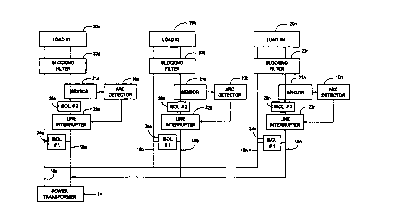
Turning now to the drawings and referring initially to FIG. 1, arcing fault
detectors 10a, lOb ... lOn are connected to n branches of an electrical
distribution system
12 having a utility company power transformer 14 as a source of electric
power. The
electrical distribution system 12 includes line conductors 16a, 16b ... 16n
and neutral
conductors 18a, 18b ... 18n which distribute electrical power to loads 20a,
20b ... 20n
through corresponding sensors 21a, 21b ... 21n, line interrupters 22a, 22b ...
22n, and
blocking filters 23a, 23b ... 23n. The line conductors 16 and a neutral
conductors 18 are
typically at 240 volts or 120 volts, and a frequency of 60 Hz.
Each of the line interrupters 22 is preferably a circuit breaker which
includes an
overload trip mechanism having a thermal/magnetic characteristic which trips
the breaker
contacts to an open circuit condition in response to a given overload
condition, to
disconnect the corresponding load 20 from the power source, as is known in the
art. It is
also known to provide the circuit breaker 22 with ground fault interrupter
circuitry
CA 02278708 1999-07-21
WO 98!35237 PCT/US98/01266
13
responding to a line or neutral-to-ground fault to energize a trip solenoid
which trips the
circuit breaker and opens the contacts.
The sensors 21 monitor the rate of change of electrical current in the
respective
line conductors 16 and produce signals representing the rate of change. The
rate-of
change signal from each sensor 21 is supplied to the corresponding arcing
detector 10,
which produces a pulse each time the rate-of change signal increases above a
selected
threshold. The rate-of change signal and/or the pulses produced therefrom are
filtered to
eliminate signals or pulses outside a selected frequency range. The final
pulses are then
monitored to detect when the number of pulses that occur within a selected
time interval
exceeds a predetermined threshold. In the event that the threshold is
exceeded, the
detector 10 generates an arcing-fault-detection signal that can be used to
trip the
corresponding line interrupter 22.
In one embodiment of the present invention, the sensor 21 comprises a toroidal
sensor having an annular core encompassing the current-carrying load line,
with the
I5 sensing coil wound helically on the care. The core is made of magnetic
material such as
a fernte, iron, or molded permeable powder capable of responding to rapid
changes in
flux. A preferred sensor uses a ferrite core wound with 200 turns of 24-36
gauge copper
wire to form the sensing coil. An air gap may be cut into the core to reduce
the
permeability to about 30. The core material preferably does not saturate
during the
2o relatively high currents produced by parallel arcs, so that arc detection
is still possible at
those high current levels.
Other means for sensing the rate of change of the current in a line conductor
are
contemplated by the present invention. By Faraday's Law, any coil produces a
voltage
proportional to the rate of change in magnetic flux passing through the coil.
The current
25 associated with an arcing fault generates a magnetic flux around the
conductor, and the
coil of the sensor 21 intersects this flux to produce a signal. Other suitable
sensors
include a toroidal transformer with a core of magnetic material or an air
core, an inductor
or a transformer with a laminated core of magnetic material, and inductors
mounted on
printed circuit boards. Various configurations for the sensor core are
contemplated by
30 the present invention and include toroids which have air gaps in their
bodies.
CA 02278708 1999-07-21
WO 98/35237 PCT/L1S98/01266
14
Preferably, the rate-of change signal produced by the sensor 21 represents
only
fluctuations in the rate of change within a selected frequency band. The
sensor bandpass
characteristic is preferably such that the lower frequency cut-off point
rejects the power
frequency signals, while the upper frequency cut-off point rejects the high
frequency
signals generated by noisy loads such as a solder gun, electric saw, electric
drill, or like
appliances, equipment, or tools. The resulting output of the sensor 21 is thus
limited to
the selected frequency band associated with arcing faults, thereby eliminating
or reducing
spurious fluctuations in the rate-of-change signal which could result in
nuisance tripping.
As an example, the sensor bandpass characteristic may have: (1) a lower
frequency cut-
off point or lower limit of 60 Hz so as to reject power frequency signals, and
(2) an upper
frequency cut-off point or upper limit of approximately I MHz so as to
effectively reject
high frequency signals associated with noisy loads. These specific frequency
cut-off
points for the sensor bandpass characteristic are by way of example only, and
other
appropriate frequency cut-off limits may be adopted depending upon actual
frequency
ranges for the power signals as well as the noisy load signals.
The desired bandpass characteristic is realized by appropriately selecting and
adjusting the self resonant frequency of the sensor. The current-type sensor
is selected to
have a predetermined self-resonant frequency which defines associated upper
and lower
frequency cut-off or roll-off points for the operational characteristics of
the sensor.
Preferably, the current-type sensor is designed to exhibit the desired
bandpass f ltering
characteristic as it operates to detect the rate of change of current
variations within the
load line being monitored. The present invention contemplates other means for
bandpass
filtering the signal output within the selected frequency band. For example, a
bandpass
filter or a combination of filters in a circuit can be used to attenuate
frequencies above or
below the cut-off points for the selected frequency band.
FIG. 2 illustrates a preferred circuit for the arcing fault detection system
of FIG.
1. The sensor 21 comprises a sensor coil T1 which is wound on a core
surrounding the
line conductor 16. Connected in parallel with the sensor coil T1 are a pair of
diodes D1
and D2 which serve as clamping devices during high-power transient conditions.
A
resistor R1 in parallel with the diodes D1 and D2 dampens self ringing of the
sensor,
during high-power transients. A pair of capacitors C1 and C2 in parallel with
the resistor
CA 02278708 1999-07-21
WO 98/35237 PCT/US98101266
R1, and a resistor R2 and an inductor L1 connected in series to the input to a
comparator
30, are tuned to assist in attaining the desired rolioff characteristics of
the filtering
network formed thereby. For example, with the illustrative values listed below
for the
components of the circuit of FIG. 2, the sensor has a passband extending from
about 10
5 KHz to about 100 KHz, with sharp rolloff at both sides of the passband.
The operation of the circuit of FIG. 2 can be more clearly understood by
reference
to the series of waveforms in FIGS. 3a through 3g. FIG. 3a is an actual
waveform from
an oscilloscope connected to a line conductor 16 carrying a-c. power at 60 Hz
and
experiencing a high-frequency disturbance beginning at time t 1. Because the
high-
frequency disturbance is within the frequency range to which the sensor 21 is
sensitive
(e.g., from about 10 KHz to about 100 KHz), the disturbance results in a burst
of high-
frequency noise in the di/dt output signal (FIG. 3b) from the sensor 21 (at
point A in the
circuit of FIG. 2), beginning at time tl. The noise burst has a relatively
high amplitude
from time tl until approximately time t2, and then continues at a low
amplitude from
15 time t2 to about time t3.
The magnitude of the rate-of-change signal from the sensor 21 is compared with
the magnitude of a fixed reference signal in a comparator 30, which produces
an output
voltage only when the magnitude of the rate-of change signal crosses that of
the
reference signal. This causes the detector to ignore low-level signals
generated by the
sensor 21. All signals having a magnitude above the threshold level set by the
magnitude
of the reference signal are amplified to a preset maximum value to reduce the
effect of a
large signal. In the comparator 30, a transistor Q 1 is normally turned on
with its base
pulled high by a resistor R3. A diode D3 changes the threshold and allows only
the
negative pulses from the sensor 21 to be delivered to the base of transistor
Ql. When the
signal to the comparator drops below the threshold level (minus 0.2 volt for
the circuit
values listed below), this causes the transistor Q 1 to turn off. This causes
the collector of
the transistor Q 1 to rise to a predetermined voltage, determined by the
supply voltage
V~~, a resistor R4 and the input impedance of a single-shot pulse generator
circuit 40.
This collector voltage is the output of the comparator circuit 30. The
collector voltage
remains high as long as the transistor Q 1 is turned off, which continues
until the signal
from the sensor 21 rises above the threshold level again. The transistor Q 1
then turns on
CA 02278708 1999-07-21
WO 9813523'7 PCTIUS98101266
16
again, causing the collector voltage to drop. The end result is a pulse output
from the
comparator, with the width of the pulse corresponding to the time interval
during which
the transistor Q 1 is turned off, which in turn corresponds to the time
interval during
which the negative-going signal from the sensor 21 remains below the threshold
level of
the comparator.
The noise burst in the sensor output is filtered to produce the waveform shown
in
FIG. 3c at point B in the circuit of FIG. 2. The waveform at point C in the
circuit of FIG.
2 is shown in FIG. 3d, and it can be seen that the amplitude has been reduced
and a d-c.
offset has been introduced by summing the filtered di/dt signal with a d-c.
bias from the
supply voltage V~~ at point C. This is the input signal to the base of the
transistor Q1.
The output of the transistor Q 1 is a series of positive-going pulses
corresponding
to the negative-going peaks in the input signal. The transistor output, at
point D in the
circuit of FIG. 2, is shown in FIG. 3e. It can be seen that the transistor
circuit functions
as a comparator by producing output pulses corresponding only to negative-
going peaks
that exceed a certain threshold in the filtered di/dt signal shown in FIG. 3c.
At this point
in the circuit, the pulses vary in both width and amplitude, as can be seen in
FIG. 3e.
To convert the output pulses of the comparator 30, which vary in both width
and
amplitude, into a series of pulses of substantially constant width and
amplitude, the
comparator output is fed to a single-shot pulse generator circuit 40. This
high-pass filter
circuit includes a pair of capacitors C3 and C4 connected in series to the
collector of the
transistor Q1, and two resistor-diode pairs connected in parallel from
opposite sides of
the capacitor C4 to ground. The pulses produced by this circuit will be
described in more
detail below in connection with the waveforms shown in FIG. 3. The output
pulses are
predominantly pulses of equal width and amplitude, although occasional larger
or smaller
pulses can result from especially large or small input pulses.
The variable-width and variable-amplitude pulses of FIG. 3e are converted to a
series of pulses of substantially constant width and amplitude by the single-
shot pulse
generator circuit 40. The output of this circuit 40, at point E in the circuit
of FIG. 2, is
shown in FIG. 3f. Although all the pulses shown in FIG. 3f are of
substantially the same
size, larger or smaller pulses may be produced by di/dt spikes that are
excessively large
or excessively small. The vast majority of the pulses at point E, however, are
CA 02278708 1999-07-21
WO 98/35237 PCT/US98/01266
17
substantially independent of the amplitude and duration of the corresponding
spikes in
the di/dt signal, provided the spikes are large enough to produce an output
pulse from the
comparator 30.
The substantially uniform pulses produced by the circuit 40 are supplied to
the
base of a transistor Q2 through a current-limiting resistor R7. A capacitor CS
connected
from the transistor base to ground improves the sharpness of the roll-off of
the bandpass
filtering. The transistor Q2 is the beginning of an integrator circuit 50 that
integrates the
pulses produced by the circuit 40. The pulses turn the transistor on and off
to charge and
discharge a capacitor C6 connected between the transistor emitter and ground.
A resistor
l0 R9 is connected in parallel with the capacitor C6, and a resistor R8
connected between
the supply voltage and the collector of the transistor Q2 determines the level
of the
charging current for the capacitor C6. The magnitude of the charge on the
capacitor C6
at any given instant represents the integral of the pulses received over a
selected time
interval. Because the pulses are substantially uniform in width and amplitude,
the
magnitude of the integral at any given instant is primarily a function of the
number of
pulses received within the selected time interval immediately preceding that
instant.
Consequently, the value of the integral can be used to determine whether an
arcing fault
has occurred.
The integral signal produced by the circuit 50 is shown in FIG. 3g, taken at
point
F in the circuit of FIG. 2. It can be seen that the integrator circuit charges
each time it
receives a pulse from the circuit 40, and then immediately begins to
discharge. The
charge accumulates only when the pulses appear at a rate sufficiently high
that the charge
produced by one pulse is less than the discharge that occurs before the next
pulse arnves.
If the pulses arrive in sufficient number and at a sufficient rate to increase
the integral
signal to a trip threshold level TR (FIG. 3g), SCRl is triggered to trip the
circuit breaker.
The circuit is designed so that this occurs only response to a di/dt signal
representing an
arcing fault.
When SCR1 is turned on, a trip solenoid S1 is energized to disconnect the load
from the circuit in the usual manner. Specifically, turning on SCR 1 causes
current to
flow from line to neutral through a diode bridge formed by diodes D7-D10,
thereby
energizing the solenoid to open the circuit breaker contacts in the line 16
and thereby
CA 02278708 1999-07-21
WO 98/35237 PCT/US98/01266
18
disconnect the protected portion of the system from the power source. The d-c.
terminals
of the diode bridge are connected across SCR/, and the voltage level is set by
a zener
diode D6 in series with a current-limiting resistor RIO. A varistor V I is
connected
across the diode bridge as a transient suppressor. A filtering capacitor C7 is
connected
across the zener diode D6. The trip circuit loses power when the circuit
breaker contacts
are opened, but of course the contacts remain open until reset.
One example of a circuit that produces the desired result described above is
the
circuit of FIG. 2 having the following values:
D1 1N4148
D2 1N4148
D3 1N4148
D4 1N4148
DS 1N4I48
D6 27v zener
R1 3.O1K
R2 1.3K
R3 174K
R4 27.4K
RS lOK
R6 l OK
R7 lOK
R8 4.2K
R9 4.75K
R10 24K
L1 3300uH
L2 SOOuH
L3 SOOuH
Cl 0.012uF
C2 0.001 uF
C3 0.001 uF
C4 0.001uF
CA 02278708 1999-07-21
WO 98!35237 PCT/US98101266
19
CS 0.001uF
C6 6.8uF
C7 1.OuF
C8 l.OuF
Q 1 2N2222A
Q2 2N2222A
SCR! CR08AS-I2 made by POWEREX-Equal
V~~ 27v
Although a circuit breaker is the most commonly used line interrupter, the
output
device may be a comparator, SCR, relay, solenoid, circuit monitor, computer
interface,
lamp, audible alarm, etc.
It will be understood that a number of modifications may be made in the
circuit of
FIG. 2. For example, the discrete bandpass filter between the sensor and the
comparator
can be replaced with an active filter using an operational amplifier. As
another example,
a single-shot timer can be used in place of the single-shot pulse generator in
the circuit of
FIG. 2. This circuit can receive the output signal from an active filter as
the trigger input
to an integrated-circuit timer, with the output of the timer supplied through
a resistor to
the same integrator circuit formed by the resistor R9 and capacitor C6 in the
circuit of
FIG. 2.
FIG. 4 illustrates a frequency-to-voltage converter circuit that can be used
in place
of all the circuitry between point A and the integrator circuit in FIG. 2. In
this circuit, the
signal from point A in FIG. 2 is supplied through a resistor Ra to a
frequency/voltage
1S converter integrated circuit SS such as an ADS37 made by Analog Devices
Inc. The
output of the integrated circuit SS is fed to a pair of comparators S6 and S7
that form a
conventional window comparator. Specifically, the output of the circuit SS is
applied to
the inverting input of a comparator S6 and to the non-inverting input of a
comparator S7.
The other inputs of the comparators S6 and S7 receive two different reference
signals A
. 20 and B which set the limits of the window, i.e., the only signals that
pass through the
window comparator are those that are less than reference A and greater than
reference B.
FIG. S illustrates an arc detector 10 for sensing the rate of change of the
line
voltage, i.e., dv/dt, rather than current. The sensor in this circuit is a
capacitor C 10
CA 02278708 1999-07-21
WO 98/35237 PCT/LIS98/01266
connected between a line conductor 16 and an inductor L 10 leading to ground.
The
inductor L10 forms part of a bandpass filter that passes only those signals
falling within
the desired frequency band, e.g., between 10 KHz and 100 KHz. The filter
network also
includes a resistor R10, a capacitor CI 1 and a second inductor L11 in
parallel with the
first inductor L10, and a resistor R11 connected between the resistor R10 and
the
capacitor C 11. The resistor R 10 dampens the ringing between the capacitor C
10 and the
inductor L10, and the resistor R11 adjusts the threshold or sensitivity of the
circuit. The
inductors L10 and L11 provide low-frequency roll-off at the upper end of the
pass band,
and a capacitor C11 provides the high-frequency roll-off at the lower end of
the pass
1 o band.
The capacitor C 10 may be constructed by attaching a dielectric to the line
bus so
that the bus forms one plate of the capacitor. The second plate of the
capacitor is attached
on the opposite side of the dielectric from the bus. The sensor circuit is
connected to the
second plate.
15 The output of the bandpass filter described above is supplied to a
comparator 60
to eliminate signals below a selected threshold, and to limit large signals to
a preselected
maximum amplitude. The filter output is applied to the inverting input of the
comparator
60, through the resistor R11, while the non-inverting input receives a
reference signal set
by a voltage divider formed by a pair of resistors R 12 and R 13 connected
between V
2o and ground. The comparator 60 eliminates very low levels of signal received
from the
sensor. The comparator 60 is normally off when there is no arcing on the line
conductor
16, and thus the comparator output is low. When the voltage signal from the
sensor is
more negative than the reference input (e.g., -0.2 volts), the output from the
comparator
goes high, and a forward bias is applied to the transistor Q2 that drives the
integrator
circuit. A capacitor C 12 connected from the base of transistor Q2 to -V~~
filters out high
frequency noise. A diode D 11 is connected between the comparator output and
the base
of the transistor Q2 to block negative signals that would discharge the
capacitor C12
prematurely. The rest of the circuit of FIG. 5 is identical to that of FIG. 2.
When a fault occurs, it is desirable to isolate the branch of the distribution
system
in which the arcing fault occurred from the rest of the distribution system.
In the system
of FIG. 1, such isolation is provided by isolator #1 (24a, 24b...24n) and/or
isolator #2
CA 02278708 1999-07-21
WO 98135237 PCTIUS98101266
21
(25a, 25b...25n). Isolator #1 is designed for use in a system using a current-
type sensor,
as shown in FIG. 2, while isolator #2 is designed for use in a system using a
voltage-type
sensor, as shown in FIG. 5. Both isolator #1 and #2 may be used in a system
having both
a current- and a voltage-type sensor.
As shown in FIG. 2, isolator #1 comprises a capacitor C8 connected between the
load line 16 and the neutral line 18 in each branch of the distribution
system. The
capacitor C8 is located between the line interrupter 22 and the power source
14 to
provide a low impedance path for an arcing fault from the line conductor 16 to
the
neutral conductor 18, independent of the impedance of the load 20. More
specifically,
the capacitor C8 is designed to effectively short high-frequency arcing fault
signals from
line conductors 16 to neutral conductors 18, thus preventing a series path
from being
created between branch circuits and preventing the erroneous detection of
arcing faults in
other branch circuits. For example, with reference to FIG. 1, the isolator #1
will prevent
high frequency arcing fault signals on line conductor 16a from crossing over
to line
conductor 16b. Accordingly, an arcing fault signal on line conductor 16a will
properly
trigger line interrupter 22a but will not trigger line interrupter 22b.
As shown in FIG. 5, isolator #2 comprises an inductor L2 in the load line 16
for
each branch circuit. Each inductor L2 is located between the line interrupter
22 and the
sensor 21 to provide an impedance for the current produced by an arcing fault.
The arcing fault detection system also includes a blocking filter 23 in each
branch
circuit for blocking false arcing fault signals or other nuisance output
signals generated
by normal operation of the load 20. Each blocking filter 23 is connected
between the
sensor 21 and the load 20 in each branch circuit to prevent false arcing fault
signals from
being delivered to the sensor 21. As seen in FIGS. 2 and 5, the preferred
blocking filter
includes a pair of capacitors C9a and C9b connected between the load line 16
and the
neutral line 18 of each branch circuit. An inductor L3 is connected in the
load line 16
between the two capacitors C9a and C9b. Preferably, the capacitors C9a and C9b
have a
rating across the line of about 0.47 uF. The inductor L3 has a rating for 15
amps at 500
uH and dimensions of about 1.5" diameter and 1.313" in length (e.g., Dale IHV
15-500).
These values, of course, can be adjusted for the power rating of the
electrical system and
the loads 20.
CA 02278708 1999-07-21
WO 98135237 PCT/US98I01266
22
The capacitor C9a creates a low impedance path for any series arcing that
occurs
upstream of that capacitor, such as arcing within the wall upstream of a noisy
load. This
permits series arcing to be detected in the branch containing the blocking
filter. The
inductor L3 creates an impedance that does most of the attenuation of the
signal created
by a noisy load. This inductor is sized to carry the load current of the
device, which is
typically I S or 20 amperes. The second capacitor C9b reduces the amount of
inductance
required in the inductor L3, by creating a low impedance path across the load
20.
One of the advantages of the blocking filter 23 is that it can be used locally
on a
particular branch circuit that is known to connect to a load 20 which is
noisy. The
expense of using the blocking filter 23 is reduced since it can be used only
where needed.
The blocking filter 23 also allows easy retrofitting to existing electrical
distribution
systems in residences and commercial space.
Although the above system has been described in connection with an ordinary
120 volt system, it is applicable to the voltages of any standard, including
12, 120, 240,
i5 480, 600 and 18500 volts. The system is suitable for use in residential,
commercial and
industrial applications, single-shot or multiphase systems and at all
frequencies for a-c. as
well as d-c. This system is applicable to automotive, aviation, and marine
needs,
separately derived sources such as generators or UPS, and capacitor banks
needing
incipient fault protection.
FIG. 6 illustrates a test circuit that may be used in an arcing fault
detection system
according to principles of the present invention. A test wire 82 passes
through the
sensing coil 21 together with the line conductor 1 ba. The test wire 82 is
connected to a
free running oscillator 84, which is adapted to produce a current in the test
wire 82
simulating an arcing fault, preferably an alternating current with a frequency
of about 10
kHz to 100 kHz. The simulated arcing fault passing through the test wire 82 is
detected
by sensor 21, which in turn sends a signal to the arcing fault detector
circuit i0 in the
same manner shown generally in FIG. 1. The arcing fault detector circuit 10 is
preferably
the same circuit shown in FIG. 2, but it will be appreciated any circuit which
detects
arcing faults may be used. The arcing fault detector circuit thereafter
processes the signal
3o produced by the sensor 21 in response to the test signal, produces a trip
signal and
CA 02278708 1999-07-21
WO 98/35237 PCTIUS98/OI266
23
triggers the line interrupter 22 (FIG. 2) in the same manner as it would for
an actual
arcing fault.
The oscillator 84 may be manually controlled through operation of a push-to-
test
switch 86. An operator may start the oscillator and introduce a current in the
test wire 82
by depressing the push-to-test switch 86, and subsequently stop the oscillator
by
releasing the push-to-test switch 86. Moreover, a self-test or automatic test
can be used
instead of the manual test described above. For example, the switch can
include a timer
for automatically starting and stopping the oscillator 84 at preselected
intervals.
An alternative test circuit 90 which may be used in arcing fault detection
systems
according to principles of the present invention is illustrated in FIG. 7. A
first terminal
92 is connected to the line conductor and a second terminal 94 is connected to
the neutral
conductor of a selected branch circuit of an electrical distribution system
having an
arcing fault detector, as in FIG. 1. A relay 96 is connected between the first
and second
terminals 92 and 94. The relay 96 contains a pair of electrical contacts 98
and a relay
coil 100. A diode 102 and a resistor 104 are connected between the second
terminal 94
and the relay coil 100. A capacitor 106 is connected between the second
terminal 94 and
the electrical contacts 98. When the first and second terminals 92, 94 are
attached to the
line and neutral conductors of the selected branch circuit, alternating
current from the
branch circuit is introduced into the test circuit 90 and energizes the relay
96. The diode
102 thereafter causes the relay coil 100 to drop every half cycle, causing the
electrical
contacts 98 to rapidly open and close, once every cycle. This chattering
effect of the
electrical contacts 98 produces a signal on the line conductor which simulates
an arcing
fault condition. The simulated arcing fault condition is thereafter detected
by the sensor
21 (FIG. 1 ) and processed by the arcing fault detector circuit 10 in the same
manner as an
actual arcing fault.
The relay 96 preferably comprises a Class 8501 Type KL-12 24VAC available
from Square D Company, but it may comprise any comparable relay known in the
art.
The capacitor 106 preferably has a value of about 0.47 p.F and is provided to
increase the
strength of the simulated arcing fault signal. The resistor 104 is provided to
drop the 120
VAC of the branch circuit down to 24 VAC for the relay 96.
CA 02278708 1999-07-21
WO 98/35237 PCT/US98101266
24
In one embodiment, the test circuit 90 is removably attachable to the line and
neutral conductors of a selected branch circuit. This enables a user to
externally remove
and attach the test circuit to a selected branch circuit as often as needed or
desired to test
the arcing fault detection system. Alternatively, the test circuit 90 may be
housed
together with the arcing fault detector circuit in a common module.
A flow chart for testing an arcing fault detection system according to
principles of
the present invention is illustrated in FIG. 8. Block 62 designates the
initiation of a
diagnostic test within the arcing fault detection system. The initiation step
62 may be
accomplished automatically or under operator control. When the diagnostic test
is
initiated, a signal generator 64 provides a test signal 65 to a sensor 21. The
test signal is
designed to simulate the occurrence of an arcing fault. The signal generator
64 may
comprise the oscillator 84 described in relation to FIG. 6, the test circuit
90 described in
relation to FIG. 7 or any other means for producing a test signal 65
simulating an arcing
fault. The sensor 21 preferably comprises a toroidal current sensing coil
substantially the
same as depicted in FIG. 6. The sensor 21 receives the test signal 65 and
produces a rate-
of change signal 68. The rate-of change signal 68 is processed by the arcing
fault
detection circuit 10 in the manner heretofore described to determine whether
or not the
test signal 65 represents an arcing fault. In addition, the sensor 21 also
monitors the line
conductor of a selected branch circuit for the occurrence of "true" arcing
faults.
The arc detection circuit I O thereafter provides an output to a diagnostic
test
integrator 72 indicating that an arcing fault either was detected or was not
detected. The
diagnostic test integrator also receives a signal from block 62 indicating
whether or not
the system is in test. Thus, either of four possible conditions will be
received by the
diagnostic test integrator 72: ( 1 ) the system is in test and an arcing fault
was detected;
(2) the system is in test and no arcing fault was detected; (3) the system is
not in test and
an arcing fault was detected; or (4) the system is not in test and no arcing
fault was
detected. The diagnostic test integrator 72 will produce a trip signal to trip
open the
contacts of a line interrupter 22 if either condition (2) or (3) occurs. Thus,
a trip signal
will be produced not only when a true arcing fault is present, but also when
an arcing
fault should have been indicated during the test protocol as a sign of
operability and yet
CA 02278708 1999-07-21
WO 98135237 PCTIUS98/01266
was not so indicated. Conversely, the diagnostic test integrator 72 will not
produce a trip
signal if either condition ( 1 ) or (4) occurs.
Where the sensor 21 comprises a toroidal winding, the arcing fault detection
system may also be tested by testing the resistance of the winding. This may
be
accomplished by inputting a test signal having a known voltage through the
winding and
comparing the resistance of the winding to a known value to deternune whether
the
winding is operating properly. Both of these steps may be accomplished while
the sensor
21 is in operation. If the winding is found to be operating outside of an
acceptable range
above or below the known value, a trip signal is generated to interrupt the
current
10 flowing in the branch circuit associated with the sensor 21. If the winding
is found to be
operating properly, no trip signal is generated. In a preferred embodiment,
the presence
or absence of a trip signal resulting from testing the resistance of the
winding is
independent of the presence or absence of a trip signal from the diagnostic
test integrator
72 of FIG. 8. For example, if no trip signal is produced because the coil is
found to be
15 operating properly as a result of the resistance test, a trip signal may
nevertheless still be
produced by the diagnostic test integrator 72 of FIG. 8 if either condition
{2) or (3)
occurs. Conversely, if a trip signal is produced by the resistance test
because the coil
resistance is not within proper limits, the line interrupter 22 will be
triggered to interrupt
the current in the branch circuit regardless of whether the diagnostic test
integrator 72 of
20 FIG. 8 has produced a trip signal.
FIG. 9 shows a three phase, four wire electrical distribution system 110
adapted
to distribute electrical power from a utility company power source (not shown)
to various
loads (not shown). Reference numerals 112, 114 and 116 designate three
respective
phase lines and reference numeral 118 designates a neutral line of the
electrical
25 distribution system 110. In industrial applications, each of the phase
lines generally
comprises a large bus bar which may be about eight inches in width and carry a
current
from 50 amps up to approximately 6,000 amps. Current transformers (CTs) 120,
122 and
124 having their primary windings connected to the respective phase lines 112,
114 and
116 are provided to step down the current to 5 amps on secondary lines 126a,
126b and
126c. Secondary lines 126a, 126b and I26c typically comprise #16 AWG
electrical
wires.
CA 02278708 1999-07-21
WO 98/35237 PCT/US98/01266
26
Power monitoring equipment 129 may be provided to monitor the electrical
distribution system 110 via one or more of the secondary lines 126a, 126b and
126c. A
sensor 130 is coupled to the secondary line 126c and is adapted to monitor the
rate-of
change of electrical current flowing through the secondary line 126c and
produce a signal
representing the rate of change. The sensor 130 may be coupled to any one of
the
secondary lines 126a, 126b or 126c. Alternatively, second and third sensors
may be
provided to monitor any two or all three of the secondary lines 126a, 126b or
126c. In
using sensors) connected to the relatively small secondary lines of a current
transformer
rather than to the large bus bars used in industrial applications, the sensor
130 is much
smaller than prior art systems and may be installed more easily and much less
expensively
than prior art systems.
The sizes and current ratings heretofore described are intended to reflect
those
found in a typical industrial system, but it will be appreciated that the
values heretofore
described are exemplary only. Moreover, the present invention is not limited
to three-
phase, four-wire systems, but may be used with single-phase, three-wire
systems or any
other electrical power distribution system known in the art. Although the
present
invention is particularly adapted for industrial systems, it will be
appreciated that the
present invention may also be used in residential or commercial systems having
a current
transformer connected to the phase or line buses.
The rate-of change signal from the sensor 130 is supplied to an arcing fault
detector circuit 132, which produces a pulse each time the rate-of-change
signal increases
above a selected threshold. The rate-of change signal and/or the pulses
produced
therefrom are filtered to eliminate signals or pulses outside a selected
frequency range.
The final pulses are then monitored to detect when the number of pulses that
occur
within a selected time interval exceeds a predetermined threshold. In the
event that the
threshold is exceeded, the arc detector circuit 132 energizes a trip solenoid
{not shown)
which triggers the appropriate line interrupter 136a, 136b or 136c to
interrupt the current
flowing in the respective line conductor 112, 114 or 116.
In an alternative embodiment, the power monitoring equipment 129 is capable of
independently energizing a trip solenoid which triggers the Iine interrupters
136a, 136b
or 136c. In this case, if the arcing fault detector circuitry 132 determines
that an arcing
CA 02278708 1999-07-21
WO 98J35237 PCTlLTS98/01266
27
fault has occurred, it may indirectly trigger the line interrupter 136 by
sending a signal
131 to the power monitoring equipment rather than directly to the line
interrupters.
Each of the line interrupters 136 is preferably a circuit breaker which
includes an
overload trip mechanism having a thermal/magnetic characteristic which trips
the breaker
contacts to an open circuit condition in response to a given overload
condition, to
disconnect the corresponding load from the power source, as is known in the
art. The
line interrupters may also be equipped with ground fault interrupter circuitry
responding
to a line or neutral-to-ground fault to energize a trip solenoid which trips
the circuit
breaker and interrupt the current in line conductor 112, 114 or 116.
FIG. 10 depicts a panelboard 210 including an integrated protection system
according to one embodiment of the present invention. As used herein, the term
"panelboard" is intended to encompass electrical distribution devices having
current
capacities suitable for either residential, commercial or industrial uses. The
panelboard
210 receives electrical power from a utility source through line buses L100
and L200 and a
neutral bus N and distributes the power to loads in a plurality of branch
circuits defined
by line conductors 216a, 216b, 216c...216n and neutral conductors (not shown).
The line
conductors 216x, 216b, 216c...216n are electrically connected to one of the
line buses
L100, L200 and the neutral conductors are electrically connected to the
neutral bus N.
The panelboard 210 comprises a framework for attaching various circuit
protection
devices to the line and neutral conductors in either of the branch circuits.
In the embodiment shown in FIG. 10, the integrated protection system includes
a
plurality of line interrupters 218a, 218b, 218c...218n and arcing fault
detector modules
220a, 220b, 220c...220n (hereinafter "AFD modules"). Each of the line
interrupters
218a, 218b, 218c...218n is designed to protect the branch circuit to which
they are
connected from overcurrents by disconnecting the load from the power source in
response to the occurrence of an overload or short circuit in the branch
circuit. The line
interrupters rnay be plugged onto or bolted to one of the line buses L 100 or
L200 as
shown in FIGS. 10 or 11, or they may be mounted separately within the
panelboard 210
and connected to one of the line buses L 100 or L200 by wire. The line
interrupters may
comprise a circuit breaker, fuse, relay, automatic switch or any suitable
means known in
the art.
CA 02278708 1999-07-21
WO 98135237 PCT/US98/01266
28
Turning now to FIG. 11, the integrated protection system of FIG. 10 is shown
in
another embodiment using an isolation module 222 at the distribution panel.
The
isolation module 222 is designed to ensure that arcing fault signals are
"isolated" to the
branch circuit in which they occur. For example, the isolation device 222
shown in FIG.
S I 1 ensures that arcing fault signals present on line conductor 216a do not
cross over to
line conductor 216b, and vice versa. A series of bus bar tabs T1 and T2 extend
in
alternating fashion along the length of distribution center 200. Each of the
tabs T1 are
electrically connected to line bus L100 and each of the tabs T2 are
electrically connected
to line bus L200. (The electrical connection between tabs T 1, T2 and line
buses L 100,
L200 is not visible in FIG. 11.) The isolation module 222 is electrically
connected to the
neutral bus N through pig-tail wire 219. The isolation module 222 comprises a
"two-
pole" module, connected to one of the tab pairs T1, T2 {not visible in FIG.
11), thus
electrically connected to both line buses L100 and L200. It will be
appreciated, however,
that isolation may be provided by one or two "single-pole" isolation modules
(not
shown), each connected to one of the line buses L100 or L200 and the neutral
bus N. In
either case, it will further be appreciated that the isolation modules) 222
may be
connected to the line buses L 100 and/or L200 by wire or other suitable means
known in
the art rather than as described above.
The electrical distribution system may also include individual isolation
modules
(not shown) for one or more of the individual branch circuits instead of the
dual-pole
isolation module 222 shown in FIG. 11. However, if individual isolation
modules are
desired, they must be positioned on the power source side of an arcing fault
detector in
any given branch circuit. For example, if branch isolation modules are used in
FIG. 11,
they must be positioned on the power source side of arcing fault detector
modules 220a,
220b, 220c or 220d.
The exterior housing of the two-pole isolation module 222 is illustrated in
more
detail in FIG. 16. Jaws J 1 and J2 on one side of the isolation module 222 are
each
adapted to plug onto one of the bus bar tabs T1, T2 of the distribution panel
and thus
provide an electrical connection to respective line buses L100 and L200. For
instance,
jaw J 1 may be electrically connected to line bus L 100 through connection to
bus bar tab
T1 and jaw J2 may be electrically connected to line bus L200 through
connection to bus
CA 02278708 1999-07-21
WO 98/35237 PCT/US98I01266
29
bar tab T2. Rail clips 225 on another side of the isolation module 222 are
adapted to
plug onto a mounting rail in the panelboard to help retain the isolation
module 222 firmly
in position in the panelboard. Pig-tail wire 219 connects the device to the
neutral bus N.
As will be described below, a window 251 in a top wall 252 of the housing
allows a user
to see an LED inside the device.
FIG. 17 depicts an electrical circuit for implementing the two-pole isolation
module 222 described in relation to FIGs. 11 and 16. As shown in FIG. 17, the
two-pole
isolation module 222 is connected to supply source 230 via line buses L100 and
L200
and neutral bus N. The isolation module 222 includes both surge protection
circuitry
(section 1 ) and isolation circuitry (section 2). However, it will be
appreciated that
module 222 may contain only isolation circuitry.
Referring initially to the surge protection circuitry (section 1) and, more
specifically, to the portion of section 1 located between the line bus L100
and neutral bus
N, there is provided a plurality of fuses Fl, F2, F3 connected between the
line bus L100
and nodes 201, 202, and 203 respectively. Varistors V 11, V 12, and V 13 are
connected
between nodes 201, 202, and 203, respectively, and the neutral bus N.
Preferably, the
varistors are metal oxide varistors using zinc oxide. Resistors R21, R22, R23
are
connected between nodes 201, 202, and 203, respectively, and node 204.
Fuses Fl, F2, and F3 open if the respective varistors V 11, V 12, and V 13
fail, that
is if a destructive surge occurs. Resistors R21, R22, and R23 form a
resistance ladder
which develops a voltage across display resistor R31. Diode D11 provides a
forward bias
between node 204 and the first display 236.
Now referring to the remainder of the surge protection circuitry {section 1 )
located between the line bus L200 and the neutral bus N, there is provided a
plurality of
fuses F4, F5 and F6 connected between the line bus L200 and nodes 205, 206 and
207
respectively. Varistors V 14, V 15 and V 16 are connected between nodes 205,
206 and
207, respectively, and the neutral bus N. Resistors R4, RS and R6 are
connected between
node 205, 206 and 207 respectively and node 208. The fuses F4, F5 and F6 are
designed
to open if the respective varistors V 14, V 15 and V 16 fail.
Display 236 comprises a resistor R31 connected in parallel with a light
emitting
diode LED1 visible through an opening 251 in a top wall 252 of isolation
module 222
CA 02278708 1999-07-21
WO 98135237 PCT/LTS98I01266
(shown in FIG. 16). LED1 provides for monitoring the status condition of
varistor and
fuse pairs such as V 11 and F 1. The intensity of LED 1 decreases when a fuse
is blown.
When only a predetermined number of varistor and fuse pairs remain
operational, LED 1
will extinguish entirely to signal for replacement of the surge protection
circuitry.
Specifically, the Iight output of LED 1 varies with the operating condition of
each
varistor and fuse pair. Display 236 uses the first plurality of resistors R21,
R22 and R23,
the second plurality of resistors R4, RS and R6, diode D1 I, resistor R31 and
LED1 to
indicate when the circuit is operating correctly. The resistance ladder of the
first set of
resistors R21-R23 monitors the fuses F1, F2 and F3 on line bus L100 and the
second set
10 of resistors R24-R2b monitors the fuses F4, FS and F6 and the line bus
L200. Line buses
L100 and L200 each develop a voltage across resistor R31 that is proportional
to the
number of conducting fuses Fl, F2, F3, F4, F5, F6. Only when a preselected
number of
these fuses are intact will sufficient voltage be available to forward bias
LED1 to emit a
signal to indicate that the surge protection circuitry is operational.
15 The above-described surge arrestor circuit is designed to limit the voltage
between line bus L100 and neutral bus N upon the occurrence of a voltage
surge. The
operation of the surge arrestor circuit is described in detail in U.S. Patent
No. 5,412,526,
hereby incorporated by reference.
Referring next to the isolation circuitry (section 2) of FIG. 17 and, more
20 specifically, to the portion of section 2 located between the line bus L100
and neutral bus
N, there is provided a fuse F7 connected between the line bus L 100 and a node
209. A
filter 240 consisting of a capacitor C21 in series with a resistor R9, is
connected between
the node 209 and the neutral bus N. Filter 240 is designed to effectively
short high-
frequency arcing fault signals from line bus L100 to neutral bus N, thus
preventing arcing
25 fault signals on line bus L100 from crossing over to line bus L200. In
completing the
arcing fault signal path from line bus L100 to neutral bus N, the filter 240
accomplishes
two functions. First, it prevents an arcing fault detector (not shown) on line
bus L200
from detecting a "false" arcing fault signal on line bus L200. Second, it
increases the
signal strength at an arcing fault detector (not shown) positioned on Iine bus
L 100 on a
30 load side of filter 240. Varistor V 17 is connected between the node 209
and the neutral
bus N. Varistor V 17 provides a degree of surge protection for the isolation
circuitry
CA 02278708 1999-07-21
WO 98/35237 PCTlUS98/OI266
31
connected between the line bus L100 and the neutral bus N. A resistor R7 and a
diode
D 12 are connected in series between the node 209 and a display 238.
Referring now to the remainder of the isolation circuitry (section 2) located
between line bus L200 and neutral bus N, there is provided a fuse F8 connected
between
the line bus L200 and a node 211. A filter 242 consisting of a capacitor C22
in series
with a resistor R30 is connected between node 211 and the neutral bus N.
Filter 242 is
designed to complete the arcing fault signal path from line bus L200 to
neutral bus N by
effectively shorting high frequency arcing fault signals from the line bus
L200 to neutral
bus N. Thus, similar to the filter 240 described above, the filter 242
prevents an arcing
fault detector (not shown) on line bus L100 from detecting a "false" arcing
fault signal on
line bus L100, and increases the signal strength at an arcing fault detector
(not shown)
positioned on line bus L200 on a load side of filter 242. A varistor V 18
provides a
degree of surge protection for the isolator circuitry connected between line
bus L200 and
neutral bus N. Resistor R8 is connected between node 2I 1 and display 238.
Display 238 consists of a resistor R32 connected in parallel with an LED2.
Display 238 provides a means for monitoring the operating status of the
isolation
circuitry. Should fuse F4 or F8 blow for any reason, causing a loss of
isolator
functionality, the LED2 will turn off. LED2 is visible through an opening 251
in the top
wall 252 of the isolation module 22 (shown in FIG. 16).
Refernng now to FIG. 12, there is depicted a panelboard 210 including an
integrated protection system according to another embodiment of the present
invention.
In this embodiment, the arcing fault detection and line interrupting functions
described
above are accomplished by combination arcing fault detector and line
interrupter
modules 224a, 224b, 224c...224n {hereinafter "combination modules"). Each of
the
combination modules is associated with one of the branch circuits of the
electrical
distribution system and includes both arcing fault detection circuitry and a
line
interrupter. The combination modules 224x, 224b, 224c...224n may be plugged
onto or
bolted to one of the line buses L100 or L200 as shown in FIGS. 12 and 13, or
they may be
mounted separately within the panelboard 210 and connected to the line buses L
100 or
L200 by wire. As shown in FIG. 13, the integrated protection system may also
include
an isolation module 222 for electrically isolating arcing fault signals to the
branch circuit
CA 02278708 1999-07-21
WO 98/35237 PCTIUS98/01266
32
on which they occurred, as described in relation to FIG. 11. Branch isolation
may also be
achieved by isolation circuitry within the combination modules 224a, 224b,
224c...224n.
In either case, the isolation module 222 or combination modules 224a...n may
also
include surge protection circuitry to protect the line buses or either of the
branch circuits
from voltage surges.
Similarly to the line interrupters described in relation to FIGs. 10 and 11,
the
combination module 224 shown in FIG. 12 or 13 may comprise a relay, fuse,
automatic
switch or circuit breaker combined with an arcing fault detector. In a
preferred
embodiment, the combination module 224 comprises a circuit breaker with arcing
fault
detection capability.
In the embodiment shown in FIG. 10, arcing fault detection capability is
provided
by the sensing coil 221 and associated electronic components 292. It is
preferred that the
electronic components 292 detect arcing faults in the manner of the AFD module
220
described in relation to FIGs. 4-8. However, it will be appreciated that the
electronic
components 292 may vary in configuration or operate differently than those of
the AFD
module 220. Moreover, in embodiments in which the circuit breaker 218 has GFI
capability, the electronic components 292 may reflect any configuration known
in the art
for sensing ground faults. At any rate, the electronic components 292 are
designed to
produce an "AFD" signal (or "GFI" signal, if applicable) in response to
detection of an
arcing fault or ground fault. The AFD or GFI signal causes a magnetic field to
be created
around a trip solenoid 295, causing a plunger 297 to be drawn to the right.
The plunger
297 is connected to a trip link 299, which in turn is connected to the
armature 274, such
that movement of the plunger 297 causes the armature 274 to be drawn to the
right.
Movement of the armature 274 to the right causes the trip lever 276 to be
released and
the current path through the circuit breaker 218 to be interrupted.
Now referring to FIGs. 14 and 15, there is depicted a panelboard 210 including
an
integrated protection system according to still another embodiment of the
present
invention. In this embodiment, the arcing fault detection and line
interrupting functions
described above are accomplished by separate arcing fault detector modules
220a, 220b,
3o 220c...220n and line interrupter modules 218a, 218b, 218c...218n
substantially as
described in relation to FIGs. 10 and 11. However, in this embodiment, the
arcing fault
CA 02278708 1999-07-21
WO 98/35237 PCTlUS981012b6
33
detector modules 220a, 220b, 220c...220n are attached externally to the line
interrupter
modules 218a, 218b, 218c...218n rather than being mounted to one of the
positions in the
panelboard 210. The line interrupter modules 218a, 218b, 218c...218n may be
plugged
onto or bolted to one of the line buses L100 or L200 as shown in FIGs.lO and
11, or they
y 5 may be mounted separately within the panelboard 210 and connected to one
of the line
buses L100 or L200 by wire. The integrated protection system may also include
isolation
modules) 222 and/or branch isolation means substantially as described in
relation to
FIG. 11. In either case, the isolation modules) 222 or branch isolation means
may
include surge protection circuitry to protect the line buses or either of the
branch circuits
from voltage surges.
Now turning to FIGs. 18 and 19, there is depicted an AFD module 220 which
may be utilized as one of the AFD modules 220a...220n in FIG. 10 or 11. The
AFD
module 220 comprises a housing 231 which is adapted to be connected to one of
the
positions in the panelboard. A line terminal 233 is provided for connecting
the AFD
module 220 to one of the line conductors 216a...216n by wire. Line current
enters the
AFD module 220 through the line terminal 233, flows through the AFD module 220
via
internal line conductor 237 and exits the AFD module 220 via load terminal 235
before
being supplied to the load. An AFD sensor 228 surrounds the internal line
conductor 237
and senses the rate of change of electrical current flowing through the
internal line
conductor 237. The rate-of change signal from the sensor 228 is supplied to
the AFD
circuit 234, which produces a pulse each time the rate-of change signal
increases above a
selected threshold. The rate-of change signal and/or the pulses produced
therefrom are
filtered to eliminate signals or pulses outside a selected frequency range.
The final pulses
are then monitored to detect when the number of pulses that occur within a
selected time
interval exceeds a predetermined threshold. In the event that the threshold is
exceeded,
the detector 234 generates an arcing-fault-detection signal that can be used
to trip the line
interrupter 230. The line interrupter 230 in the AFD module 220 is designed to
interrupt
power in the branch circuit resulting from an arcing fault, not an overcurrent
(overload or
short circuit) condition. Accordingly, as shown in FIGs. 18 and 19, it is
preferred that
the line interrupter 230 in the AFD module 220 comprise a relay rather than a
circuit
breaker such as that described in relation to FIGS. 13 and 14.
CA 02278708 1999-07-21
WO 98135237 PCTlITS98/01266
34
In one embodiment of the present invention, the line interrupters comprise
circuit
breakers which are connected to the panelboard by means of a housing 561 as
depicted in
FIG. 20. The miniature circuit breaker housing 561 is comprised of an
electrically-
insulating base 563 closed at one face by a detachable cover 565 which
together enclose
the components of a miniature circuit breaker, which may comprise a standard
circuit
breaker, a ground fault interrupter module, an arcing fault detection system
or any
combination thereof. In embodiments including an arcing fault detection
system, the
arcing fault detection system will preferably be that described in relation to
FIG. 1, but it
will be appreciated that alternative types of arcing fault detection systems
may be
enclosed within the miniature circuit breaker housing 561. A clip 577 is
provided for
mounting the housing 561 to a mounting bracket 587 of a panelboard 575 of an
electrical
distribution system. An electrically-conductive jaw-like terminal 569a or bolt
terminal
569b extends through the base 563 to be externally connected to a line bus bar
573 within
the panelboard 575. Similarly, a panel neutral conductor 579 extends through
the
housing 561 for connection to a neutral bar 581 in the panelboard 575.
External
connections to the line and neutral conductors leading to a load center of a
branch circuit
of the electrical distribution system are provided through a load line
conductor 583 and
load neutral conductor 585, respectively. An operating handle 588 and test
button 567
are mounted through separate openings in the base 563 for external manual
operation of
the miniature circuit breaker.
Turning now to FIG. 21, there is provided a diagram of a miniature circuit
breaker 522 adapted to be housed within the miniature circuit breaker housing
of FIG. 20
including standard circuit breaker components and an arcing fault detection
system
according to one embodiment of the present invention. As depicted in FIG. 21,
the
miniature circuit breaker 522 is in a closed position, enabling line current
to flow
completely through the circuit breaker and toward a load center of a
designated branch
circuit. Line current enters the circuit breaker 522 through the jaw-like
terminal 569a
and flows through a stationary contact carrier 562 integral with the terminal
569a. The
stationary contact carrier 562 has a stationary contact 566 mounted thereon.
When in the
3o closed position, the stationary contact 566 abuts against a movable contact
568 which is
mounted to a movable contact carrier 564. Line current thereby flows from the
stationary
CA 02278708 2003-10-03
WO 98/35237 PCT/US98I01266
contact carrier 562 to the movable contact carrier 564 through the stationary
and movable
contacts 566 and 568, respectively.
A pigtail conductor 589 is electrically connected at one end to the movable
contact carrier 564 and at another end to a yoke 572, enabling line current to
flow from
5 the movable contact carrier 564 to the yoke 572 when the circuit breaker 522
is in a
closed position. A bimetal conductor assembly 590 composed of two dissimilar
thermostat materials is electrically connected to the yoke 572. The bimetal
conductor
assembly 590 includes a conductive plate 591 at one end which is electrically
connected
to an internal conductor 593. When the circuit breaker 522 is in the closed
position,
1 o electrical current flows from the yoke 572 through the bimetal conductor
assembly 590 to
the conductive plate 591 and through the internal conductor 593. Thereafter,
current
flowing through the internal conductor 593 passes through a sensing coil 521
substantially as described in relation to FIG. 1 which monitors the rate of
change of
electrical current flowing through the circuit breaker 522. After exiting the
sensing coil
15 521, the line current flows to load terminal block 570 to which the load
line conductor
583 (FIG. 20) may be attached to provide the line current to a load. The load
terminal
block 570 is defined by two conductive plates adapted to be clamped together
by a screw.
The load line conductor 583 may be attached by inserting it between two
conductive
plates and tightening the screw of the load terminal block 570.
20 The miniature circuit breaker 522 also includes a neutral terminal block
571 to
which the load neutral conductor 585 (FIG. 20) may be attached in a similar
fashion as
the load line conductor 583 is attached to the load terminal block 570. The
miniature
circuit breaker fiirther includes an internal neutral conductor 603
electrically connected at
one end to the circuit board 596 and at another end to the panel neutral
conductor 579
25 described in relation to FIG. 20. In embodiments with ground fault
interruption (GFI)
circuitry, the panel neutral conductor 579 is routed through the sensor 521
along with the
internal line conductor 593 to permit sensing of an imbalance of current flow
between the
internal line and neutral conductors 593 and 603 as is known in the art. A
more complete
description of GFI circuitry is disclosed in U.S. Patent No. 5,446,431.
CA 02278708 1999-07-21
WO 98135237 PCT/US98/01266
36
Now turning to FIG. 22, the miniature circuit breaker 522 is shown in an open
position. In the open position, the movable contact carrier 564 is rotated
away from the
stationary contact carrier 562, causing the movable contact S68 to become
separated from
the stationary contact 566 and interrupt the electric current flowing through
the circuit
breaker 522. The circuit breaker 522 may be tripped open in any of several
ways,
including manual control and in response to thermally and electromagnetically-
sensed
overload conditions and ground fault conditions. As the mechanism for tripping
open the
circuit breaker 522 is described in detail in Patent No. 5,446,431, it will be
described
only briefly herein.
The miniature circuit breaker 522 may be moved between the open and closed
positions by a user manually moving the operating handle 588 to the right or
left,
respectfully, causing corresponding movement of the top of the movable contact
carrier
564 to the left or right of an equilibrium position. A toggle spring 578 is
connected at
one end to the operating handle 588 and at another end to the bottom of the
movable
contact carrier 564. When the top of the movable contact carrier 564 is left
of the
equilibrium position, the toggle spring 578 serves to bias the bottom of the
movable
contact carrier 564 to the closed position. Conversely, when the top of the
movable
contact carrier 564 is right of the equilibrium position, the toggle spring
578 biases the
bottom of the movable contact carrier to the open position.
The miniature circuit breaker S22 may also be tripped open in response to
sensing
various types of fault conditions. Upon the occurrence of a moderately
sustained
overload condition when the contacts 566 and 568 are in a closed position, the
bimetal
conductor assembly 590 becomes heated and bends to the right. Bending of the
bimetal
conductor assembly 590 causes an armature 574 and yoke 572 to swing
counterclockwise
and release a trip lever 576. The trip lever S76 rotates clockwise about pin
580, causing
the toggle spring 578 to pull the bottom of the movable contact carrier 564
away from the
stationary contact 566 and interrupt the current path.
Similarly, upon the occurrence of an extensive current overload condition, a
high
magnetic flux field is created around the yoke 572. The armature 574 is drawn
toward
the yoke 572 by the magnetic field, causing the trip lever 576 to become
released from
the armature 574. As described in relation to thermal trips, release of the
trip lever 576
. ,
CA 02278708 1999-07-21
WO 98135237 PCT/US98J01266
37
from the armature 574 causes the toggle spring to pull the bottom of the
movable contact
carrier 564 away from the stationary contact 566 and interrupt the current
path.
Finally, electronic components 592 mounted on a circuit board 596 are provided
for processing the signal output of the sensor 521 and determining whether an
arcing
fault condition or ground fault condition is present. The electronic
components 592 for
sensing arcing faults are preferably the same as that described in relation to
FIG. 2 or 5,
but it will be appreciated that any configuration of electronic components 592
known in
the art for detecting arcing faults may be provided. Similarly, the electronic
components
592 may reflect any configuration known in the art for sensing ground faults.
At any
rate, the electronic components 592 are designed to produce either an "AFD"
and/or
"GFI" trip signal corresponding to whether the circuit breaker 522 is designed
to sense
arcing faults and/or ground faults. In response to generation of either an AFD
or a GFI
trip signal, a magnetic field is created around a trip solenoid 595, causing a
plunger 597
to be drawn to the right. The plunger 597 is connected to a trip link 599,
which in turn is
connected to the armature 574, such that movement of the plunger 597 causes
the
armature 574 to be drawn to the right. As previously described, movement of
the
armature 574 to the right causes the trip lever 576 to be released and the
current path
through the circuit breaker 522 to be interrupted.
A flag armature 605 is connected to the trip lever 576 by a reset pin 609.
When
the trip lever 576 becomes released from the armature 574 in response to
either of the
several types of trip conditions described above, the flag armature 605 is
moved to the
right and becomes visible through a lens 607, thus providing an external trip
indication
external to the housing of the circuit breaker 522.
As depicted in FIG. 21, the circuit breaker 522 further includes a trip
indicator
594 independent from the flag armature 605 for specifically indicating when
the circuit
breaker 522 has been tripped open by an arcing fault or ground fault. The trip
indicator
594 is connected at one end to the circuit board 596 upon which are mounted
the
electronic components 592 described above for detecting arcing faults and/or
ground
faults. Upon generation of either an AFD or GFI trip signal, the circuit
breaker S22 is
tripped open and the trip indicator 594 provides a visible signal 598 external
to the
housing of the circuit breaker 522.
CA 02278708 1999-07-21
WO 98135237 PCT/US98/01266
38
Referring now to FIG. 23, the trip indicator 594 will be described in greater
detail. The trip indicator 594 comprises a light source 600, a light conduit
602 and an
aperture 604. The light source may comprise a light emitting diode (LED), neon
bulb or
any other suitable light source known in the art. The light source is attached
to the circuit
board 596 within the circuit breaker housing and is illuminated in response to
the
generation of either an AFD or GFI trip signal. Illumination of the light
source 600
causes light waves to emanate outwardly from the light source in a direction
approximated by the arrows 606. A light conduit 602 having one end aligned
with the
light source subsequently intercepts the light waves emanating from the light
source.
The light conduit may comprise a light tube (FIGS. 21 and 23), a fiber optic
cable (FIG.
24), an open portion of the circuit breaker housing (FIG. 25) or any other
suitable means
known in the art, but preferably is composed of a non-conductive material so
that it does
not interfere with the current carrying parts within the circuit breaker. Upon
reaching the
conduit, the light waves are redirected back and forth between the inner walls
of the
conduit as approximated by the arrows 606 in FIG. 23, ultimately reaching the
aperture
604 at the other end of the conduit and emanating beyond the outer surface 606
of the
circuit breaker housing. Accordingly, a user may determine the circuit breaker
trip
condition by observing the exterior of the circuit breaker housing. Generally,
the
presence of light emanating outside of the housing indicates that a trip
condition has
occurred, while the absence of light indicates that a trip condition has not
occurred or that
the circuit breaker has tripped due to electromechanical or thermal
conditions.
Preferably, where the circuit breaker 522 contains both AFD and GFI sensing
circuitry, the trip indicator 594 will indicate which type of fault condition
caused the
circuit to be interrupted. This may be accomplished by utilizing multiple
light sources,
each responding to a different respective AFD or GFI trip signal.
Additionally, it is
preferred that the light sources or single light source may be mufti-colored
so that
illumination of a particular color will identify whether the circuit breaker
522 was tripped
open by an arcing fault or ground fault. A representative circuit for
accomplishing this
purpose is shown at FIG. 26, which utilizes a red LED 613 for indicating a GFI
fault
condition and a yellow LED 629 for indicating an AFD fault condition. Of
course, it will
CA 02278708 1999-07-21
WO 98/35137 PCT/US98I01266
39
be appreciated that the color configuration of LEDs may be reversed or that
alternative
colors other than red and yellow may be utilized.
In the embodiment shown in FIG. 26, each of the LEDs 613 and 629 is
electrically connected between the line and neutral conductors on a line side
of the circuit
breaker, isolated from the load side of the circuit breaker by respective
optotriacs 611 and
625 to prevent any potential leak paths from line to load after the breaker
has tripped.
Activation of a GFI (or AFD) trip signal by the electronic components 592
(FIG. 21 )
causes an electrical current to flow through the optotriac 611 (or 625) which
in turn
provides a current path from line to neutral through the LED 613 (or 629). To
keep the
LED 613 or 629 illuminated after the breaker has tripped, the optotriacs 611
or 625 are
latched to a conductive state by powering them directly from the line side of
the breaker,
thus providing a minimum current through the line side of the optotriac 611 or
625
independent of any signaling from the GFI or AFD circuitry.
Under normal operating conditions, the capacitor b17 has no discharge path,
and
therefore it retains a voltage level specified by the zener diode 615. Once
the optotriac
driver 611 (or 625) is triggered by GFI (or AFD) circuitry, the capacitor 617
is able to
discharge through the LED 613 (or 629) only if the optotriac driver 611 {or
625) is
activated on a negative half cycle. The RC time constant provided by resistor
619 (or
627) and capacitor 617 serves to hold the current above the maximum holding
current of
the optotriac 611 (or 625). This provides a forward-biased current path to LED
613 or
629 for the duration of the negative half cycle. On the next positive half
cycle, the
capacitor 617 will charge to the level specified by the zener diode 615. The
positive half
cycle will also provide current to keep the optotriac 611 or 625 conducting.
If the
optotriac driver 611 or 625 were initially triggered by the GFI or AFD
circuitry on a
positive half cycle, current from the positive half cycle would provide the
current
necessary to keep the optotriac driver 611 or 625 conducting. Once the voltage
level of
the positive half cycle starts falling below the voltage level that the
capacitor 617 was
charged to, the capacitor 617 will start discharging through the LED 613 or
629. The RC
time constant provided by a resistor 619 (or 627) and the capacitor 617 serves
to hold the
current above the maximum holding current of the optotriac 611 (or 625).
CA 02278708 1999-07-21
WO 98/35237 PCT/US98/01266
A zener diode 615 is used as a voltage regulator for keeping the operation of
the
circuit insensitive to fluctuations in line voltage. A rectifier 623 is used
to protect the
LED 613 from large reverse voltages. A resistor 621 is used as a current
limiter for the
current flowing through the LED 613 or 629.
Turning now to FIG. 27, there is depicted an alternative embodiment of the
trip
indicator 594 in which a plunger 610 is attached to the circuit board 596
within the
circuit breaker housing. The plunger 610 is movable between a retracted
position and an
extended position in response to the activation of the trip signal. When in
the extended
position, a colored tip 612 extends outwardly from the plunger 6I0 in response
to the
10 generation of a trip signal. A light tube 602 is aligned such that one end
of the light tube
602 is adjacent to the colored tip 612 when the plunger is in the extended
position. The
other end of the light tube extends beyond the outer surface 606 of the
circuit breaker
housing. Ambient light external to the circuit breaker housing enters the
light tube 602
through the aperture 604 and is reflected back and forth along the length of
the light tube
15 602 until reaching the plunger 610. Upon reaching the plunger 610, the
light is reflected
back toward the aperture 604. When a trip signal has been generated causing
the colored
tip 612 to extend outwardly from the plunger 610, a reflection of colored
light is
propagated from the colored tip 612 along the surface of the light tube 602
and emanates
out of the aperture 604.
20 Turning now to FIG. 28, there is depicted another alternative embodiment of
the
trip indicator 594 in which a bimetal disk 614 is attached to the circuit
board 596 within
the circuit breaker housing. The bimetal disk 614 is thermally movable between
a
generally flat position and a convex position in response to the activation of
the trip
signal. When in the convex position, a colored top 616 of the bimetal disk 614
extends
25 outwardly from the circuit board 596 in response to the generation of a
trip signal. A
light tube 602 is aligned such that one end of the light tube is adjacent to
the colored top
616 when it is in the convex position. The other end of the light tube extends
beyond the
outer surface 606 of the circuit breaker housing. Ambient light external to
the circuit
breaker housing enters the sight tube 602 through the aperture 604 and is
reflected back
30 and forth along the length of the light tube 602 until reaching the bimetal
disk 614. Upon
reaching the bimetal disk 614, the light is reflected hack toward the aperture
604. When
CA 02278708 1999-07-21
WO 98/35237 PCTIUS98/01266
4l
a trip signal has been generated, causing the colored top 616 of the bimetal
disk 614 to
extend outwardly from the circuit board 596, a reflection of colored light is
propagated
from the colored top 616 along the surface of the Iight tube 602 and emanates
out of the
aperture 604.
As described in relation to FIG. 26, it is preferred that the trip indicator
is capable
of distinguishing whether the trip signal has been generated by AFD or GFI
circuitry.
This may be accomplished by utilizing multiple trip indicators of the type
shown in FIGs.
27 or 28, each responding to the generation of either an AFD or GFI trip
signal. Each of
the respective trip indicators may include a different color of colored tip
(FIG. 27) or
colored top (FIG. 28) such that reflection of light from a particular color
identifies the
particular type of fault condition which caused the circuit breaker to trip
open.
Now referring to FIGS. 29 and 30, there are depicted further embodiments of
the
trip indicator 594 including a reset button 618 and a test switch 626. As
shown in
FIG. 29, the reset button 618 is integral with the end of the light tube 602
extending
beyond the circuit breaker housing 608, but it will be appreciated that the
reset button
may be located in a different position and physically independent from the
light tube 602.
The reset button 618 is designed to be depressed inwardly by a user in the
direction of
arrow 620, thereby causing the light tube to be moved inwardly within the
circuit breaker
housing 608. The trip indicator 594 may also include a coil spring 622 which
is
2o compressed when the reset button 618 is depressed and springs back when the
reset
button 618 is released. The light tube 602 will preferably be composed of a
relatively
stiff material, such as polycarbonate or acrylic plastic, so that the bottom
portion of the
light tube 602 is moved inwardly in the direction of arrow 620 when the reset
button 618
is depressed. The bottom portion of the light tube 602 thereafter physically
pushes down
on the plunger 610 (FIG. 29) or bimetal disk 6l4 (FIG. 30), restoring the
plunger or
bimetal disk back to its respective untripped position (e.g. retracted or
generally flat
position).
The trip indicator 594 may also be provided with a test switch 626 including a
first contact b28, a second contact 630 and a push-to-test button for
activating the test
switch 626. The push-to-test button may comprise the reset button 618 as shown
in
FIGS. 29 and 30 or may comprise an independent push-to-test button 638 as
shown in
CA 02278708 1999-07-21
WO 98135237 PCT/IIS98/01266
42
FIG. 3I . In either case, upon depression of the push-to-test button, the
first contact 628
is pressed down upon the second contact 630, forming an electrical connection
between
the two contacts 628, 630. The second contact 630 is connected to a current
source 632,
while the first contact 628 is connected to the electronic components 592
within the
circuit breaker. Thus, depression of the push-to-test button 618 causes the
current source
632 to become electrically connected to the electronic components 592 within
the circuit
breaker. The electronic components 592 thereafter interpret the influx of
current from
the current source as a fault condition and activate a trip signal in response
thereto.
Activation of the trip signal causes the trip indicator 594 to produce a light
signal or
reflected light signal external to the circuit breaker housing as described
above. Upon
release of the push-to-test button 618, the first contact 628 returns to its
initial position
apart from the second contact 630, causing an interruption of the electrical
path between
the current source 632 and the electronic components 592 within the circuit
breaker.
In embodiments such as those depicted in FIGs. 29 and 30 in which a single
button 618 is used as both a reset button and a push-to-test button, a time-
delay circuit
must be included within the electronic components 592 within the circuit
breaker.
Inasmuch as time delay circuits are well known in the art, they will not be
described in
detail herein. Suffice it to say that upon depression of the reset button/push-
to-test button
618, the electronic components 592 within the circuit breaker will not
activate a trip
signal until the reset button/push-to-test button is depressed for a
predetermined period of
time. Accordingly, a user intending to reset the trip indicator 594 may press
down briefly
upon the reset button 618 without inadvertently activating a trip signal.
A still further embodiment of the trip indicator 594 is depicted in FIG. 32,
in
which the test switch may be activated by twisting rather than pushing down
upon the
light tube 602. In this embodiment, a cam 634 is attached to the light tube
602. Rotation
of the light tube 602 causes the cam 634 to push the first contact 628 toward
the second
contact 630 and ultimately form an electrical connection between a current
source and
the electronic components 592 within the circuit breaker. Then, as described
above in
relation to FIGs. 29 and 30, the electronic components 592 activate a trip
signal which in
turn causes the trip indicator 594 to produce a light signal or reflected
light signal
external to the circuit breaker housing. As shown in FIG. 32, the above-
described twist-
CA 02278708 1999-07-21
WO 98135237 PCT/US98/01266
43
to-test feature may be combined with the push-to-reset feature discussed in
relation to
FIGs. 29 and 30. Moreover, the trip indicator 594 may include a twist-to-reset
feature
combined with a push-to-test feature, a push-to-reset feature and a push-to-
test feature, or
a twist-to-reset feature and a twist-to-test feature.
FIG. 33 illustrates the relationship among components for tripping a circuit
breaker in response to sensing arcing faults, ground faults and overloads. To
detect the
occurrence of an arcing fault when the circuit breaker contacts are in a
closed position, an
arcing fault sensor 740 monitors a rate-of-change of electrical current in the
line
conductor 734 and provides a signal representing the rate-of change to a trip
circuit 742
comprising electronic circuitry mounted on circuit board 742. The arcing fault
detection
circuitry 743 in the trip circuit 742 analyzes the signal for characteristics
of an arcing
fault. When the arcing fault detection circuitry 743 detects the presence of
an arcing
fault, it sends a trip signal to the latching mechanism 720 to trip the
circuit breaker 710.
CA 02278708 1999-07-21
WO 98/35237 PCT/US98101266
44
To detect the occurrence of a ground fault when the circuit breaker contacts
are in
a closed position, a ground fault sensor 741 detects the difference in current
in the line
conductor 734 and a neutral conductor 733 and provides a signal representing
the
difference to the trip circuit 742. Ground fault detection circuitry 745 in
the trip circuit
742 analyzes the signal for characteristics of a ground fault. If the ground
fault detection
circuitry 745 detects a ground fault, the trip circuit 742 sends a trip signal
to the latching
mechanism 720 to trip the circuit breaker 710 in the same fashion as described
above.
To detect the occurrence of an overload when the circuit breaker contacts are
in a
closed position, the overload circuitry 747 of the trip circuit 742 samples
the current
flowing through the line conductor 734. The overload circuitry 747 analyzes
current
samples for characteristics of an overload. If the trip circuit 742 detects an
overload, the
trip circuit sends a trip signal to the latching mechanism 720 to trip the
circuit breaker in
the same fashion as described above.
The flexibility of electronic components of the trip circuit provide the
circuit
breaker with a variety of detection features. The circuit breaker may be
provided with
circuitry to open the breaker in response to an arcing fault, ground fault or
overload. The
electronic components of the trip circuit may be modified to detect only one
of the above
conditions, or all of the listed conditions. In every possible case, the trip
circuit will
provide the latching mechanism 720 with a trip signal in response to the
occurrence of a
detected condition.
FIG. 33 includes an enlarged side elevation of one embodiment of the latching
mechanism 720. The latching mechanism 720 contains a coil 750, plunger 752,
latch
..,..._.~..-,._..._..~........_r..~_ .. _.__... r _.....
CA 02278708 1999-07-21
WO 98!35237 PCT/US98/01266
plate 754 and bias spring 756. The coil 750 is a typical solenoid, and the
plunger 752 is
positioned for movement into the coil 750. The latch plate 754 of FIG. 33 has
a plastic
rectangular block portion 760 partially surrounded by a thin metal jacket 762.
The
plastic portion 760 has an orifice end interlocking with a steel cylindrical
plunger 752 to
form the plunger/latch plate assembly. When the latching mechanism 720 is in
the
engaged position, the seat end of the latch plate 754 engages the trip lever
718. The
metal jacket 762 of the latch plate 754 supplies a smooth, non-corrosive
surface for easy
motion within the breaker case 728 and away from the trip lever 718. The
smooth
motion from the engaged position to the released position gives the breaker
710
10 consistent tripping action.
The latching mechanism of FIG. 33 further includes a bias spring 756
surrounding the plunger 752. One end of the bias spring 756 abuts the latch
plate 754
and the other end abuts the coil 750. The bias spring 756 may abut the
exterior portion
of the coil housing 758, or the bias spring may be positioned within the coil
750 (see
15 FIG. 34). The bias spring 756 pushes the plunger/latch plate assembly 752
and 754 away
from the coil 750 to bias them toward the engaged position for seating the
trip lever 718
on the latch plate 754.
When a overload, ground fault or arcing fault is detected by the trip circuit,
the
trip circuit sends a trip signal to the coil 750. The trip signal energizes
the coil 750 and
20 creates a magnetic field within the coil 750. The magnetic field draws the
plunger 752
further into the coil 750. The plunger's motion into the coil 750 moves the
plunger/latch
plate assembly 752 and 754 to the right and compresses the bias spring 756.
This motion
pulls the latch plate 754 away from the trip lever 718 and disengages the trip
lever 718
from its seat on the latch plate 754. The trip lever 718 slides off of the
latch plate 754
25 into the tripped position, thereby causing the separation of the movable
contact 726 from
the stationary contact 724 and opening the circuit breaker 710.
FIG. 33 also illustrates an additional feature for the tripping mechanism 720.
An
upwardly extending stop 764 is formed on the latch plate 754. The stop 764
limits the
movement of the plunger/latch plate assembly within the case 728. The stop 764
halts
30 the motion of the plunger/latch plate assembly 752 and 754 to the left
after the assembly
has reached the position necessary to engage the trip lever 718. The stop 764
also halts
CA 02278708 1999-07-21
WO 98/35237 PCT/US98/01266
46
the motion of the assembly 752 and 754 to the right after it has reached the
position
necessary to disengage the trip lever 718 from its seat on the latch plate
754.
Once the circuit breaker is in the released position, causing the trip lever
718 to
be in the tripped position, current stops flowing from the line terminal to
the load
terminal. Current no longer flows through the line conductor. The current
sensors 740
and 741 stop providing signals to the trip circuit because no current is
available to
measure. The trip circuit ceases transmitting a trip signal to the tripping
mechanism 720,
so the coil 750 is no longer energized. The magnetic field in the coil 750
vanishes, and
the bias spring 756 returns the plunger 752 and latch plate 754 to their
engaged positions.
To reset the circuit breaker, a user manually moves a handle to the typical
reset
position, moving the trip lever 7I8 upward to its latched position. The upper
edge of the
trip lever 718 moves the plunger/latch plate 752 and 754 toward the coil 750
by
compressing the bias spring 756. When the trip lever 718 reaches its upper
position, the
plunger/latch plate 754 return to their engaged position, seating the trip
lever 718 in its
15 latched position.
There are several alternative embodiments for the integrated latch mechanism
formed by the plungerllatch plate assembly 752 and 754 and the trip lever 718.
FIG. 34
shows another embodiment for the plunger/Iatch plate assembly 752 and 754. In
this
case, the plunger 752 performs the function of the latch plate in the engaged
position by
2o providing a seat to mechanically engage the trip lever 718. The plunger 752
is a steel
cylinder with a flattened seat end for mechanically engagement with the trip
lever 718.
The smooth surfaces of the plunger 752 eliminate friction with the trip lever
718 and the
breaker case 728 when the plunger moves from the engaged to released position.
To
implement this arrangement, the plunger 752 has slight shoulder stops 761 to
captivate
25 the bias spring 756.
FIG. 35a-35c illustrate further embodiments of the plunger/latch plate
assembly
752 and 754. In FIG. 35a, a flat metal latch plate 754 has a notched end 768
interlocking
with the groove end 766 of the plunger 752. As depicted in FIG. 35b, the
CA 02278708 1999-07-21
WO 98135237 PCT/US98101266
47
notched end 768 of the latch plate 754 abuts the bias spring 756 and acts as a
stop by
limiting the movement of the plunger/latch plate assembly 752 and 754 in the
breaker
case 728. The latch plate 754 in FIG. 35a has a folded seat end to engage the
trip lever
718. Alternative embodiments for the seat end of the latch plate 754 are a
rounded end
of FIG. 35b and an L-shaped end turned away from the trip lever 718 as
illustrated by
FIG. 35c. For consistent tripping action, the surfaces of the above latch
plates 754 are
buffed smooth and rounded to allow the latch plate 754 to slide smoothly in
the case 728
and away from the trip Lever 718.
FIG. 36a-36c depict a plunger/latch plate assembly 752 and 754 with a latch
plate
754 functioning as a self contained bias spring. In this arrangement, the
latch plate 754
itself performs the biasing function of the bias spring 756 in the previous
embodiments.
The latch plate 754 is composed of a flexible metal which compresses under
force and
returns to its original form when the force is removed. The latch plate 754
with the self
contained bias spring in its relaxed state is in the engaged position. When
the plunger
752 is drawn into the coil so, the latch plate 754 is compressed or flexed
such that the
seat end engaging the trip lever 718 moves toward the coil 750 allowing the
trip 718 to
slide from its latched to tripped position interrupting the circuit
FIG. 36a shows one embodiment of the latch plate 754 functioning as a self
contained spring. The latch plate 754 has a U-shaped portion 770 positioned
between the
grooved end of the plunger 752 and the coil housing 758. When the latching
mechanism
is in the engaged position, the U-shaped portion 770 in a relaxed state
maintaining the
engagement between the latch plate 754 and trip lever 718. When the plunger
752 is
drawn into the coil 750, the U-shaped portion 770 of the latch plate 754
compresses. The
motion of the plunger pulls the seat end of latch plate 754 to the right,
causing the trip
lever 718 to slide off the latch plate 754 and open the circuit.
FIG. 36b and 36c illustrate an alternative embodiment of the latch plate 754
with
the self contained spring. In this embodiment, the self contained spring is an
L-shaped
portion of the latch plate with its leg 772 turned away from the trip lever
718. When the
latching mechanism is in the engaged position, the leg 772 is in a relaxed
state
maintaining the engagement between the latch plate 754 and the trip lever 718
as shown
in FIG. 36b. In FIG. 36c, the coil 750 pulls the plunger/latch plate assembly
752 and 754
CA 02278708 1999-07-21
WO 98/35237 PCT/I1S98101266
48
to the right flexing the leg 772 and moving the seat end of the latch plate
754 to the right.
Because of the motion of the seat end of the latch plate 754 toward the coil,
the trip lever
718 slides off its seat on the latch plate 754 opening the circuit.
FIG. 37 illustrates a modified embodiment of the circuit breaker having the
line
conductor 734 wrapped around the latching mechanism 720 as a loop 776 for high
magnetic tripping. When the current through the circuit breaker rises to a
high level, i.e.,
above a preselected level, the current in the loop 776 produces a magnetic
field that pulls
the plunger 752 into the coil 750. The movement of the plunger 752 into the
coil 750
opens the circuit as described in detail above. The high magnetic tripping of
the circuit
breaker occurs as soon as the current through the line conductor 732 passes
the threshold
level.
FIG. 38 shows a similar embodiment of the electronically controlled circuit
breaker with integrated latch tripping. In FIG. 38, the latching mechanism 720
consists
of an armature 780, yoke 782 and a trip coil 784 wrapped around the yoke 782.
The
current path in this embodiment passes from the moveable contact carrier 716
through a
flexible conductor 786 {or pigtail) which connects the current path to a yoke
782, which,
in turn, is electrically connected to the line conductor 734. FIG. 38
illustrates an
embodiment of the circuit breaker 710 with a ground fault detection sensor
741. Other
embodiments are contemplated including arcing fault and overcurrent detection
circuitry.
As disclosed above, the ground fault sensor 741 in FIG. 38 senses the
imbalance
of current flow between the line and neutral conductors 734 and 733. When the
trip
circuit determines the presence of a ground fault, a trip signal is sent to
the trip coil 784.
The trip coil 784 is energized by the trip signal in the same manner as the
coil was
energized as disclosed above. The energized trip coil 784 generates a magnetic
field
about the yoke 782. In the preferred embodiment, the trip coil 784 has
wrappings to
produce a magnetic field of approximately 1500 A turns.
The armature 780 is pivotally cradled at its upper end 788 in the arms 790 of
the
yoke 782. An air gap 796 separates the armature 780 from the yoke 782. An
armature
spring 792 resiliently restrains the armature 780 from swinging relative to
the yoke 782.
When the latching mechanism is in the engaged position, the trip lever 718
engages the
armature by resting on a seat 794 notched into the armature 780. When the trip
coil 784
..._..~..~..~~,.....r.~.,~...w...-w..v..
CA 02278708 1999-07-21
WO 98!35237 PCT/ITS98101266
49
produces a magnetic field, the armature 780 is drawn toward the yoke 782
causing the
armature 780 to swing counterclockwise closing the air gap 796 moving the
latching
mechanism to its released position. When the armature 780 swings to the right,
the trip
lever 718 is released from its seat 794 on the armature 780. As disclosed
above, the trip
lever 718 swings clockwise to open the circuit.
The circuit breaker may be reset in its traditional fashion. With the circuit
open, a
trip signal is no longer sent to the trip coil 784, so the magnetic field
dissipates and the
armature 780 returns to its engaged position. A user manually moves the handle
722 to
the typical reset position, rotating the trip lever 718 counterclockwise. The
trip lever 718
engages the armature 780 moving it toward the yoke 782. When the trip lever
718
reaches its upper position, the trip lever 718 returns to its seat 794 on the
armature 780
resetting the trip lever in its latched position and resetting the circuit
breaker.
As shown in FIG. 39, a dual-pole isolation device 810 is connected to a first
line
bus L801, a second line bus L802, and a neutral bus N of an electrical
distribution
1S network. The electrical distribution network delivers electrical power from
a power
source (not shown) to branch circuits B 1, B2, B3 and B4 each including
respective line
conductors L803, L804, L805 and L806 and a neutral conductor N for delivering
electrical power to respective loads 834, 832, 830 and 828. Line interrupters
812, 814,
816 and 818 are attached to the respective line conductors L803, L804, L805
and L806 of
each branch circuit between the power source and the load. The line bus L802
is
connected to line interrupters 812 and 814 while line bus L801 is connected to
interrupters 816 and 818. The line interrupters 812, 814, 816, and 818 are
designed to
break the current flow in a particular branch circuit B 1, B2, B3, and B4 when
an arcing
fault is detected in the branch circuit. However, it will be appreciated that
the electrical
distribution network heretofore described is exemplary only.
The dual-pole isolation device 810 is designed to ensure that high frequency
arcing fault signals present on either of the branch circuits B 1, B2, B3 or
B4 are isolated
to the branch circuit on which the arcing fault occurred, thus ensuring that
only the line
interrupter associated with the branch circuit in which the arcing fault
occurred is tripped.
More specifically, the isolation device 810 ensures that an arcing fault
signal present in
branch circuit B 1 will not trip line interrupters 814, 816 or 818, but rather
will trip only
CA 02278708 1999-07-21
WO 98/35237 PCT/US98/01266
line interrupter 812. Similarly, the isolation device 810 ensures that an
arcing fault signal
present in either of branch circuits B2, B3 and B4 will trip only respective
line
interrupters 814, 816 and 818. This is achieved by providing a low impedance
path from
line bus L801 to neutral bus N and from line bus L802 to neutral bus N, so
that arcing
5 fault signals in either of the branch circuits B 1, B2, B3 and B4 are
effectively shorted at
line bus L801 or L802, thus preventing "false" arcing fault signals in the
other branch
circuits. By completing the arcing fault signal path, the isolation device 810
also serves
to increase the signal strength at the arc fault detector in the branch
circuit in which the
arcing fault occurred. Preferably, the isolation device 810 also includes
surge protection
10 circuitry which protects the electrical distribution network from voltage
surges.
Turning now to FIG. 40, there is depicted a panelboard 850 which may be used
to
house the isolation device according to the present invention. As used herein,
the term
"panelboard" is intended to encompass electrical distribution devices having
current
capabilities suitable for residential, commercial, or industrial uses. The
panelboard 850
15 transmits electrical power from a utility source to a plurality of branch
circuits through
line buses L801 and L802 and a neutral bus N. Each branch circuit comprises a
line and
neutral conductor for delivering electrical power from the panelboard to a
load. As
shown in FIG. 40, the branch circuits comprise line conductors L803 and L804
and
respective neutral conductors (not shown) for delivering electrical power to
respective
20 loads (not shown}. Each of the line conductors L803 and L804 is
electrically connected
to one of the line buses L801 or L802 and the neutral conductors are
electrically
connected to the neutral bus N at the distribution panel. Each of the line
conductors
L803 and L804 are routed through respective line interrupters 856 and 858.
The line buses L801 and L802 and the neutral bus N are typically at 240 volts
or
25 120 volts, and a frequency of 60 Hz and enter the panelboard at main lugs
862 and 864.
A series of bus bar tabs T 1 and T2 extend in alternating fashion along the
length of
distribution center 865. Each of the tabs T1 are electrically connected to
line bus L801
and each of the tabs T2 are electrically connected to line bus L802. {The
electrical
connection between tabs T1, T2 and line buses L801, L802 is not visible in
FIG. 40.) A
30 dual pole isolation device 866 is connected to one of the tab pairs T1, T2,
thus is
electrically connected to both line buses L801 and L802. The dual pole
isolation device
__.__.._.w~._....._._w_~...,.o.,r.____~._.___ , _.._.. .
CA 02278708 2003-10-03
WO 98/35237 PCT/US98/01266
51
866 is electrically connected to the neutral bus N through pig-tail wire 868.
As discussed
above, the isolation device 866 is designed to ensure that arcing fault
signals are
"isolated" to the branch circuit in which they occur. For example, the
isolation device
866 shown in FIG. 40 ensures that arcing fault signals present on line
conductor L803 do
not cross over to line conductor L804, and vice versa_
Referring again to FIG. 40, each branch circuit of the panelboard includes a
line
interrupter 856 or 858 designed to disconnect the load from the power source
in any of
the branch circuits in which an arcing fault occurs. In a preferred
embodiment, each of
the line interrupters 856 or 858 comprises a circuit breaker having a trip
mechanism
which trips the breaker contacts to an open circuit condition in response to
characteristics
of arcing faults, as is known in the art. One preferred method of detecting
arcing faults is
disclosed in United States Patent 5,682,101, for "Arcing Fault Detection
System", issued
October 28,1997, and assigned to the assignee of the present invention. The
circuit
breaker may also respond to overload conditions having thermal/magnetic
characteristics,
as is known in the art. It is also known to provide the circuit breaker with
ground fault
interrupter circuitry responding to a line or neutral-to-ground fault to
energize a trip
solenoid which trips the circuit breaker and opens the contacts.
The line interrupters may comprise a circuit breaker, fuse, relay automatic
switch
or any suitable means known in the art. The line interrupters need not be the
same type
in each of the branch circuits. The line interrupters may be plugged onto or
bolted to one
of the distribution buses L80I or L802 or they may be mounted separately
within the
panelboard and connected to one of the distribution buses L80I or L802 by
wire.
CA 02278708 1999-07-21
WO 98/35237 PCT/US98101266
52
As mentioned above, the panelboard 850 includes a dual-pole isolation device
866 for electrically isolating arcing faults in the appropriate branch circuit
and for
increasing the signal strength of the arcing fault signal in the appropriate
branch circuit.
The isolation device 866 is preferably mounted near the electrical supply
source
connection within the panelboard. It may be plugged in or bolted onto the
neutral bus
and the distribution buses L801 and L802, or it may be connected to the bus
lines by
wire. Preferably, the dual-pole isolation device 866 will include surge
protection
circuitry to protect either of the distribution buses L801 or L802 from
voltage surges.
Alternatively, two single-pole isolation devices may be provided, each being
connected
to the neutral bus N and one of the distribution buses L801 or L802.
Alternatively, the electrical distribution system may include branch isolation
modules (not shown) in one or more of the individual branch circuits to
accomplish the
same function as the dual-pole isolation module 866 shown in FIG. 40. However,
if
branch isolation modules are used, the line interrupters 856 and 858 shown in
FIG. 40
must not comprise arcing fault detectors because isolation modules must be
positioned
on the power source side of an arcing fault detector in any given branch
circuit.
Accordingly,~if branch isolation modules are used, arcing fault detection must
be
provided either by separate arcing fault detector modules (not shown)
positioned on a
load side of the branch isolation modules, or by combined arcing fault
detector and
isolation modules (not shown) in which the arcing fault detector portion is
positioned on
the load side of the isolation portion.
As shown in FIG. 42, a dual-pole isolation device 924 is connected to supply
source 930 via line buses L801 and L802 and neutral bus N. The isolation
device 924
includes both surge protection circuitry (section 1) and isolation circuitry
(section 2).
However, it will be appreciated that device 924 may contain only isolation
circuitry.
Referring initially to the surge protection circuitry (section 1) and, more
specifically, to the portion of section 1 located between the line bus L801
and neutral bus
N, there is provided a plurality of fuses F1 l, F12, F13 connected between the
line bus
L801 and nodes 901, 902, and 903 respectively. Varistors V21, V22, and V23 are
connected between nodes 901, 902, and 903, respectively, and the neutral bus
N.
....~..,.._~ ._.._ , _ _...
CA 02278708 1999-07-21
WO 98135237 PCT/US98I01266
53
Preferably, the varistors are metal oxide varistors using zinc oxide.
Resistors R51, R52,
R53 are connected between nodes 901, 902, and 903, respectively, and node 904.
Fuses F1 l, FI2, and F13 open if the respective varistors V21, V22, and V23
fail,
that is if a destructive surge occurs. Resistors R51, R52, and R53 form a
resistance
ladder which develops a voltage across display resistor R61. Diode D21
provides a
forward bias between node 904 and the first display 936.
Now referring to the remainder of the surge protection circuitry (section 1 )
located between the line bus L802 and the neutral bus N, there is provided a
plurality of
fuses F14, F15 and F16 connected between the line bus L802 and nodes 905, 906
and
907 respectively. Varistors V24, V25 and V26 are connected between nodes 905,
906
and 907, respectively, and the neutral bus N. Resistors R54, R55 and R56 are
connected
between node 905, 906 and 907 respectively and node 908. The fuses FI4, FIS
and F16
are designed to open if the respective varistors V24, V25 and V26 fail.
Display 936 comprises a resistor R61 connected in parallel with a light
emitting
diode LED 1 I visible through an opening in a top wall of isolation module
866. LED 11
provides for monitoring the status condition of varistor and fuse pairs such
as V21 and
Fl 1. The intensity of LED11 decreases when a fuse is blown. When only a
predetermined number of varistor and fuse pairs remain operational, LED11 will
extinguish entirely to signal for replacement of the surge protection
circuitry.
Specifically, the light output of LEDI 1 varies with the operating condition
of
each varistor and fuse pair. Display 936 uses the first plurality of resistors
R51, R52 and
R53, the second plurality of resistors R54, R55 and R56, diode D21, resistor
R61 and
LED 11 to indicate when the circuit is operating correctly. The resistance
ladder of the
first set of resistors R51-R53 monitors the fuses Fl l, F12 and F13 on line
bus L801 and
the second set of resistors R54-R56 monitors the fuses F14, F15 and F16 and
the line bus
L802. Line buses L801 and L802 each develop a voltage across resistor R61 that
is
proportional to the number of conducting fuses F I 1, F 12, F 13, F 14, F 15,
F 16. Only
when a preselected number of these fuses are intact will sufficient voltage be
available to
forward bias LED 11 to emit a signal to indicate that the surge protection
circuitry is
operational.
CA 02278708 2003-10-03
WO 98135237 PCT/US98I01266
54
The above-described surge arrestor circuit is designed to limit the voltage
between line bus L801 and neutral bus N upon the occurrence of a voltage
surge. The
operation of the surge arrestor circuit is described i» detail in U.S. Patent
No. 5,412,526.
Referring next to the isolation circuitry (section 2) of FIG. 42 and, more
specifically, to the portion of section 2 located between the line bus L801
and neutral bus
N, there is provided a fuse F17 connected between the line bus L801 and a node
909. A
filter 940 consisting of a capacitor C51 in series with a resistor R59, is
connected
between the node 909 and the neutral bus N. Filter 940 is designed to
effectively short
high-frequency arcing fault signals from line bus L801 to neutral bus N, thus
preventing
arcing fault signals on line bus L801 from crossing over to line bus L802. In
completing
the arcing fault signal path from line bus L801 to neutral bus N, the filter
940
accomplishes two functions. First, it prevents an arcing fault detector (not
shown) on
line bus L802 from detecting a "false" arcing fault signal on line bus L802.
Second, it
increases the signal strength at an arcing fault detector (not shown)
positioned on line bus
L801 on a load side of filter 940. Varistor V27 is connected between the node
909 and
the neutral bus N. Varistor V27 provides a degree of surge protection for the
isolation
circuitry connected between the line bus L801 and the neutral bus N. A
resistor R57 and
a diode D22 are connected in series between the node 909 and a display 938.
Referring now to the remainder of the isolation circuitry (section 2) located
between line bus L802 and neutral bus N, there is provided a fuse F18
connected
- between the line bus L802 and a node 910. A filter 942 consisting of a
capacitor C52 in
series with a resistor R60 is connected between node 910 and the neutral bus
N. Filter
942 is designed to complete the arcing fault signal path from line bus L802 to
neutral bus
N by effectively shorting high frequency arcing fault signals from the line
bus L802 to
neutral bus N. Thus, similar to the filter 940 described above, the filter 942
prevents an
arcing fault detector (not shown) on line bus L80I from detecting a "false"
arcing fault
signal on line bus L801, and increases the signal strength at an arcing fault
detector (not
shown) positioned on line bus L802 on a load side of filter 942. A varistor
V28 provides
a degree of surge protection for the isolator circuitry connected between line
bus L802
and neutral bus N. Resistor R58 is connected between node 910 and display 938.
CA 02278708 1999-07-21
WO 98135237 PCTlUS98/01266
Display 938 consists of a resistor R62 connected in parallel with an LED12.
Display 938 provides a means for monitoring the operating status of the
isolation
circuitry. Should fuse F14 or F18 blow for any reason, causing a loss of
isolator
functionality, the LED 12 will turn off. LED 12 is visible through an opening
in the top
5 wall of the isolation device 866.
It will be appreciated that the design and operation of the two-pole isolation
device heretofore described may be similarly applied to single-pole isolation
devices or
multi-pole isolation devices. The circuit for a single-pole isolation device
will be
substantially similar to the above-described two-pole isolation device, the
difference
10 being that it will contain only the circuitry of sections l and 2 located
between the line
bus L801 and neutral bus N.
Thus, an electrical isolation device is provided where faults are isolated to
the
electrical branch of the electrical distribution network where they occur. The
isolation
device can be a single-pole, dual-pole or multiple-pole device and is
adaptable for use on
15 the power source side of an arcing fault detector. The device can be
constructed such
that it is adaptable for use in a variety of areas of an electrical
panelboard. The isolation
device also contains circuitry which suppresses voltage surges occurring in
the electrical
distribution network.
FIG. 43 illustrates a plan view of a circuit breaker 1001 including standard
circuit
20 breaker components and arcing fault detection components disposed within
the miniature
circuit breaker housing shown in FIG. 42. As depicted in FIG. 43, the
miniature circuit
breaker 1001 is in a closed position, enabling line current to flow completely
through the
circuit breaker and toward the load of a designated branch circuit. Line
current enters the
circuit breaker 1001 through the jaw-like terminal 1069a and flows through a
stationary
25 contact carrier 1089 integral with the jaw like terminal 1069a. The
stationary contact
carrier 1089 has a stationary contact 1002 mounted thereon. A movable contact
1003
mounted to a movable contact carrier 1091 abuts against the stationary contact
1002
when the circuit breaker 1001 is in the closed position. Line current thereby
flows from
the stationary contact carrier 1089 to the movable contact carrier 1091
through the
30 stationary and movable contacts 1002 and 1003, respectively.
CA 02278708 2003-10-03
WO 98/35237 PCT/US98/OI266
56
A pigtail conductor 1093 is electrically connected at one end to the movable
contact carrier 1091 and at another end to a yoke 1095, enabling line current
to flow from
the movable contact carrier 1091 to the yoke 1095 when contacts 1002 and 1003
are in a
closed position. A bimetal conductor 1097 composed of two dissimilar
thermostat
materials is electrically connected to the yoke 1095. The bimetal conductor
1097 is
electrically connected to an internal line conductor 1101 which is connected
to a load
terminal I I05. When contacts 1002 and 1003 are in the closed position, line
current
flows from the yoke 1095 through the bimetal conductor 1097 and through the
internal
line conductor 1101. Thereafter, current flowing through the internal line
conductor
to I 101 passes through a sensing coil 1103 which monitors the rate of change
of line
current flowing through the circuit breaker 1001. The present invention in one
aspect is
related to methods for assembling certain components associated with sensing
coil 1103.
After exiting the sensing coil 1103, the line current flows to a load terminal
1 I05
to which the load line conductor may be attached to provide the line current
to a load.
The line current is electrically connected to circuit board 1123 at connection
1 105x. The
present invention in one aspect is related to methods and apparatus for
connecting the
load line conductor to the load line terminal 1105. The miniature circuit
breaker 1001
also includes a load neutral terminal 1 I07 to which the load neutral
conductor may be
attached. The miniature circuit breaker further includes an internal neutral
conductor
electrically connected to the neutral terminal 1107 and the panel neutral
conductor
described in relation to FIG. 20. The internal neutral conductor is
electrically connected
to the circuit board 1123 at connection 1079x. The present invention in one
aspect is
related to methods and apparatus for connecting the internal neutral
conductor, panel
neutral conductor and load neutral conductor to the Load neutral terminal
1107. In
embodiments with ground fault interruption (GFI) circuitry (not shown), the
load neutral
conductor would be routed through the sensor 1103 along with the internal line
conductor 1101 to permit sensing of an imbalance of current flow between the
internal
line and neutral conductors 1101 and 1079 as is known in the art. A more
complete
description of GFI circuitry is disclosed in U.S. Patent No. 5,446,431.
CA 02278708 2003-10-03
WO 98135237 PC'T/US98I01266
57
The circuit breaker 1001 may be tripped open in any of several ways, including
manual control and in response to thermally and electromagnetically-sensed
overload
conditions and ground fault conditions. The mechanism for tripping open the
circuit
breaker 1001 is described in detail in United States Patent 5,446,431, issued
August 29,
1995, and assigned to the assignee of the present invention. Accordingly, it
will be
described only briefly herein.
The miniature circuit breaker 1001 may be moved between the open and closed
positions by a user manually moving the operating handle 1111 to the right or
left,
respectively, causing corresponding movement of the top of the movable contact
carrier
1091 to the left or right of a pivot point. A toggle spring 1 I 13 is
connected at one end to
the operating handle 1111 and at another end to the movable contact carrier
1091. When
the top of the movable contact carrier 1091 is left of the handle pivot point,
the toggle
spring 1113 serves to bias the bottom of the movable contact carrier 1091 to
the open
position. Conversely, when the top of the movable contact carrier 1091 is
right of the
pivot point, the toggle spring 1113 biases the bottom of the movable contact
cannier 1091
to the closed position.
The miniature circuit breaker 1001 is also designed to be tripped open in
response
to sensing various types of fault conditions. Upon the occurrence of a
moderately
sustained overload condition when the contacts 1002 and 1003 are in a closed
position,
the bimetal conductor 1097 becomes heated and the lower end bends to the
right. The
bimetal conductor 1097 may be adjusted by calibration screw 1133. Bending of
the
bimetal conductor 1097 by differential expansion causes an armature 1115 and
yoke
1095 to swing counterclockwise and release a trip lever 1117. The trip lever
1117 rotates
clockwise about pin 1119, causing the toggle spring 1113 to pull the bottom of
the
movable contact carrier 1091 away from the stationary contact 1002 and
intemtpt the
current path.
Similarly, upon the occurrence of an extensive current overload condition, a
high
magnetic flux field is created around the yoke 1095. The armature 1115 is
drawn toward
the yoke 1095 by the magnetic field, causing the trip lever 1117 to become
released from
the armature 1115. As described in relation to thermal trips, release of the
trip lever 1117
CA 02278708 2003-10-03
WO 98135237 PCTlUS98/01266
58
from the armature 1 I 15 causes the toggle spring 1113 to pull the bottom of
the movable
contact carrier 1091 away from the stationary contact 1002 and interrupt the
current path.
Finally, electronic components 1121 mounted on a circuit board 1123 are
provided for processing the signal output of the sensor 1103 and determining
whether an
arcing fault condition or ground fault condition are present. The electronic
components
1121 are preferably the same as those described in United States Patent
5,682,101, issued
October 28,1997, but it will be appreciated that any configuration of
electronic
components known in the art for detecting arcing faults may be provided.
Similarly, the electronic components 1121 may reflect any configuration known
in the art
for sensing ground faults. At any rate, the electronic components 1121 are
designed to
produce an "AFD" and/or "GFI" trip signal corresponding to whether the circuit
breaker
is designed to sense arcing faults and/or ground faults. In response to
generation of either
an AFD or a GFI trip signal, a magnetic field is created around a trip
solenoid 1125,
causing a plunger 1127 to be drawn to the right. The plunger 1127 is connected
to a trip
IS link 1129, which in turn is connected to the armature 1 I 15, such that
movement of the
plunger 1127 causes the armature 111 S to be drawn to the right. As previously
described, movement of the armature 1115 to the right causes the trip lever 1
I 17 to be
released and the current path through the circuit breaker 1001 to be
interrupted.
In an altennative embodiment of the present invention, the electronic
components
1121 may also be designed to generate a thermaUmagnetic trip signal in
response to
overloads or short circuits, thus obviating the need for the bimetal, yoke and
armature
associated with the prior art. This capability is described in detail in
United States Patent
5,136,457, issued August 4, 1992, and assigned to the assignee of the present
invention.
In this embodiment, the thermal/magnetic trip signal will cause the contacts
of the circuit
breaker I 001 to be opened in substantially the same manner as they would in
response to
an AFD or a GFI trip signal.
FIGS. 44 and 47 show an assembly 1010 which includes a printed circuit board
1012 (FIG. 44 only) and a housing 1014. The housing 1014 has a removable upper
section 1016 and a lower section 1018 which is connected to the circuit board
1012. The
sensing coil 1020 comprises an upper core section 1022 and a lower core
section 1024
(see FIG. 47). A winding 1026 surrounds the lower core section 1022, as best
illustrated
CA 02278708 1999-07-21
WO 98/35237 PCT/US98/01266
59
in FIG. 47. Each end of winding 1026 is connected to a respective one of the
electrically
conductive pins 1027 which continue through the housing 1014 and thus are
electrically
attached to the circuit board 1012. The upper care section 1022 interlocks
with the lower
core section 1024 to form a horizontally oriented hollow center 1060 through
which the
. 5 line conductor (or both line and neutral conductors) of the circuit
breaker are designed to
pass. The upper section 1016 of the housing 1014 has a pair of catches 1019
for
snapping onto a respective pair of ramps 1017 on the lower section 1018. Thus,
the upper
and lower sections substantially enclose the sensing coil 1020. It is feasible
to omit
upper section 1016 if desired, in which case the outer cover serves as the
upper housing.
The housing 1014 has a pair of openings 1015 through which load line terminal
1028
extends. These openings may have different configurations (e.g. compare Figs.
44 and
47 depending on the shape of the load line terminal).
Returning to FIG. 44, load line terminal 1028 has a long end 1030 and a short
end
1032. The long end 1030 is partially surrounded with insulator 1034 where it
passes
through the hollow center of sensing coil 1020. The long end 1030 is disposed
in sensing
coil 1020 so that the insulator 1034 extends beyond the sensing coil 1020 and
through the
opening 1015. Line current passes through load terminal 1036 which is
connected to the
long end 1030 of load line terminal 1028. Preferably, load terminal 1036 is
connected to
long end 1030 by a pinch weld as shown. Calibration screw 1038 is disposed in
load
terminal 1036 so that a portion of calibration screw 1038 extends past load
terminal
1036.
Power is supplied to circuit board 1012 via a connection to the load line
terminal
1028. In one embodiment, the connection is via clip 1042 for frictionally and
electrically
engaging the short end 1032 of load line terminal 1028. Alternatively, the
connection
1042 can include a leaf spring 1044 that is pinch welded to the short end 1032
of load
line terminal 1028, as shown in FIG. 45.
In a preferred embodiment illustrated in FIG. 46, lower section 1018 of
housing
1014 can include an insulating channel 1046 for insulating the calibration
screw 1038
and a screw driver inserted into the circuit breaker from the components on
the circuit
board 1012. The insulating channel 1046 is substantially U-shaped and
configured to
receive the calibration screw 1038 and to assist in the alignment of a screw
driver with
CA 02278708 1999-07-21
WO 98/35237 PCT/US98/01266
the head of calibration screw 1038. The insulating channel 1046 is connected
to or is
integral with the lower section 1018 of housing 1014.
FIG. 48 illustrates an alternative connection between the load terminal 1036
and
load line terminal 1028. In one embodiment, load terminal 1036 has a slot 1032
that is
5 configured to receive the long end 1030 of the load line terminal 1028. In
an alternative
embodiment (not shown), the load line terminal 1028 has a similar slot that is
configured
to receive the end of load terminal 1036.
FIG. 49 illustrates an alternative embodiment in which the hollow center 1060
of
sensor 1020 is oriented vertically rather than horizontally. Thus, the
terminals pass
l0 vertically rather than horizontally through the coil as in the embodiment
discussed above.
Here, a sensor bus 1054, which has a first end portion 1056 and a second end
portion
1058, is connected to circuit board 1012 through slots 1055. The sensing coil
1020 is
disposed around the first end portion 1056. Load terminal 1036 is connected to
the first
end portion 1056. Load line terminal 1028 is connected to the second end
portion 1058.
15 Preferably, both connections are made by pinch welding as shown. FIG. 50
illustrates an
alternative embodiment wherein the load line terminal 1028 and the sensor bus
1054 are
made from a single piece of metal.
FIGS. 56-58 illustrate additional constructions to those shown in FIGs. 46 and
49-
50 respectively. FIG. 56 shows a one-piece sensing coil 1014A with the hollow
center
2o oriented horizontally. The load line terminal 1028A is preassembled with
the sensing
coil 1014A and placed on the circuit board, 1012A and then pinch welded to the
load
terminal 1036A and the circuit board connector 1042A. A screw terminal may be
used to
connect the power supply as shown.
FIGS. 57 and 58 show a one-piece sensing coil ( 1014B and 1014C) with the
25 hollow center oriented vertically. In those constructions, power is
supplied through
connections either under the circuit board ( 1012B FIG. 57) or above the
circuit board
(1012C FIG. 58). The connections to the load terminal (1036B and 1036C) are
made by
pinch welding above the sensing coil (1014B and 1014C), again facilitating top-
down
assembly.
CA 02278708 1999-07-21
WO 98/35237 PCTIL1S98/01266
61
Flexible, but restrained, wire terminations are important features of the
circuit
breakers of the invention to facilitate their automated assembly. Alternative
methods of
providing such wire terminations are shown in FIGs.51-54.
A lug connection 1062 is illustrated in FIG. S 1. The lug 1062 includes a top
1064
and a hollow center 1066. The top 1064 includes a hole 1068 connecting the top
1064 to
the hollow center 1066. A neutral bus 1070 which is connected via wire 1082 to
the
panel neutral (not shown) is connected by lug 1062 to the load neutral via
wire 1078.
End 1072 of bus 1070 is positioned inside of the hollow center 1066 of the lug
1062 and
extends underneath the hole 1068. A wire binding screw 1076 is disposed in the
hole
1068 and extends through the hollow center 1066 in order to secure wire 1078
between
end 1072 of the neutral bus 1070 and bottom 1071 of hollow center 1066. A
strain relief
member 1080 is provided at end 1074 of the neutral bus 1070.
Turning to FIG. 52, there is shown a strain relief member 1080 which includes
a
top section 1084 for connecting the load neutral wire (shown as 1078 in FIG. S
1 ) and a
bottom section 1086. The top section 1084 is substantially flat and includes a
hole 1090
disposed therein. The load neutral wire is clamped between the flat section
and a second
mating plate (not shown) by means of a screw (not shown) threaded into hole
1090.
Strain relief region 1092 defines a cavity 1094 for receiving the panel
neutral wire. The
bottom section 1086 forms a cylinder 1092 which defines a cavity 1094. The top
section
1084 and the bottom section 1086 are connected together and separated by a
solid
member 1096. Connected to the top section 1084 of strain relief member 1080 is
a wire
1098 (corresponding to wire 1082 of FIG. 51). The wire 1098 extends through
the cavity
1094 formed by the bottom section 1086 and is secured therein in order to
prevent strain
on the connection of wire 1098 to top section 1084. In a preferred embodiment,
the wire
1098 is pinch welded to top section 1084 as shown.
In an alternative embodiment illustrated in FIG. 53, wire 1098 is connected to
the
solid member 1096 of the strain relief member 1080. The wire 1098 extends
through
cavity 1094 in order to prevent strain on the connection of wire 1098 to solid
member
1096. Preferably, the wire 1098 is pinch welded to solid member 1096. As
described in
FIG. 52 the load neutral wire 1078 (of FIG. 51 ) would be clamped to the upper
section
1084.
CA 02278708 1999-07-21
WO 98!35237 PCTIUS98I01266
62
In another alternative embodiment illustrated in FIG. 54, the load neutral
wire is
shown connected to the top section 1084 by a screw 1100 as previously
described in
connection with FIGS. 52-53. The panel neutral wire 1098 is connected to the
bottom
section 1086 of the strain relief member 1080. Strain relief section 1092
prevents strain
on the connection of wire 1098.
FIG. 55 illustrates an embodiment in which a slot 1106 is provided in the
outer
edge of the circuit board 1012 to receive a clip which secures load line
terminal 1028
(see FIG. 45). The bottom sections of the clip 1108 and the clamp terminal
1028 are
disposed in the slot 1106 of the circuit board 1012. Extending from the bottom
of the
clip and the clamp terminal are flanges 1110 which are configured to limit the
load line
terminal 1028 from moving in any direction except towards the center the
circuit board
1012.
Turning now to the drawings and referring initially to FIG. 59, there is shown
a
schematic block diagram of an arcing fault detection system connected to a
single branch
circuit of an electrical distribution system. It will be appreciated, however,
that the
arcing fault detection system may be connected to multiple branch circuits.
Each branch
circuit is comprised of line conductor 1510 and neutral conductor 1512 which
distribute
electrical power from a utility company power transformer 1514 to a load 1516.
The line
conductor 1510 and neutral conductor 1512 are typically at 240 volts or 120
volts, and a
frequency of 60 Hz. A sensor 1518 senses the rate of change of electrical
current on the
line conductor 1510 and sends a rate-of change signal, commonly referred to as
a di/dt
signal, to an arc detector 1520. As will be described in detail hereinafter,
the arc detector
1520 processes and evaluates the sensor signal for characteristics of arcing
faults. If the
arc detector 1520 senses the occurrence of an arcing fault, it produces a trip
signal to line
interrupter 1522, which interrupts the current in line conductor 1 S 10.
The line interrupter 1522 is preferably a circuit breaker which includes an
overload trip mechanism having a thermal/magnetic characteristic which trips
the breaker
contacts to an open circuit condition in response to a given overload
condition, to
disconnect the load 1516 from the power source, as is known in the art. It is
also known
to provide the circuit breaker 1522 with ground fault interrupter circuitry
responding to a
CA 02278708 1999-07-21
WO 98/35237 PCT/US98I01266
63
line or neutral-to-ground fault to energize a trip solenoid which trips the
circuit breaker
and opens the contacts.
The sensor 1518 preferably comprises a toroidal sensor having an annular core
encompassing the current-carrying line conductor 1510, with the sensing coil
wound
helically on the core. The core is made of magnetic material such as a
ferrite, iron, or
molded permeable powder capable of responding to rapid changes in flux. A
preferred
sensor uses a ferrite core wound with 200 turns of 24-36 gauge copper wire to
form the
sensing coil. An air gap may be cut into the core to reduce the permeability
to about 30.
The core material preferably does not saturate during the relatively high
currents
to produced by parallel arcs, so that arc detection is still possible at those
high current
levels.
Other means for sensing the rate of change of the current in a line conductor
are
contemplated by the present invention. By Faraday's Law, any coil produces a
voltage
proportional to the rate of change in magnetic flux passing through the coil.
The current
associated with an arcing fault generates a magnetic flux around the
conductor, and the
coil of the sensor 1518 intersects this flux to produce a signal. Other
suitable sensors
include a toroidal transformer with a core of magnetic material or an air
core, an inductor
or a transformer with a laminated core of magnetic material, and inductors
mounted on
printed circuit boards. Various configurations for the sensor core are
contemplated by
2o the present invention and include toroids which have air gaps in their
bodies.
An integrator 1523 integrates the di/dt signal from the sensor 1518 to produce
a
signal representing the current (i) carried by the line conductor 1510. The
integrated
di/dt signal (or i signal) is thereafter processed by a signal conditioner
1524 and
converted to a series of pulses by analog-to-digital (AID) converter 1526. The
current
pulses are then sampled at a plurality of points by sampler 1528. The sampled
current is
then processed by CPU 1530, which determines the number of certain arcing
fault
characteristics occurring within a predetermined time interval. If the number
of arcing
fault characteristics exceed a trip threshold level within the predetermined
time interval,
the CPU 1530 produces a trip signal to trigger the line interrupter 1522.
Turning now to FIG. 60, there is shown an overview flow chart of the steps
accomplished by the arcing fault detection system according to one embodiment
of the
CA 02278708 1999-07-21
WO 98135237 PCT/US98/01266
64
present invention. Each of these steps will be described in detail in relation
to FIGs. 61
through 65. Generally, however, step 1 represents the obtaining of current
samples from
the sampler 1528. Preferably, samples will be taken from either two
consecutive half-
cycles (e.g. a positive half cycle followed by a negative half-cycle, or vice
versa), two
consecutive positive half-cycles or two consecutive negative half cycles.
Moreover, it is
preferred that samples are taken at 32 points per half cycle of current, but
it will be
appreciated that an alternate number of sampling points may be used. Next, as
represented by step 2, the CPU determines the magnitude of the current peak in
each
selected half cycle. Next, as represented by step 3, the "slope", or ratio of
current peaks
from one half cycle to the next is assigned a polarity (e.g. "positive" or
"negative"), and
the number of reversals of polarity between adjacent slopes is counted.
Finally, in step 6, the number of reversals in polarity is compared to a trip
threshold level. If the number of reversals in polarity exceed the trip
threshold level, a
trip signal is sent to the line interrupter 1522 to disconnect the power
source from the
load. If the number of reversals in polarity do not exceed the trip threshold
level and
thereby do not represent an arcing fault, the above-described process repeats
itself with
newly obtained current samples until an arcing fault is detected. Preferably,
the trip
threshold level will be high enough so that reversals in polarity caused by
known load
transients do not trip the circuit breaker. In a preferred embodiment of the
present
invention, the trip threshold level is based on finding fifteen or more
reversals in polarity
per second.
In another embodiment of the present invention, the CPU 1530 detects arcing
faults by counting the number of significant waveform shape changes between
half
cycles in addition to counting the number of reversals in polarity. This is
accomplished
by performing step 3 heretofore described along with additional steps 4 and 5.
In step 4,
the CPU 1530 normalizes and autocorrelates the current samples. Normalizing is
accomplished by dividing each of the current samples by the peak current
associated with
the half cycle from which they were taken. Each of the current samples will
thereby have
a normalized magnitude less than or equal to 1. Autocorrelation is
accomplished by
comparing each one of the number of normalized current samples from one half
cycle to
the corresponding one of the number of normalized current samples in the next
selected
.. ~._Mw..-.-.~..r......~..~"~",.~..... ...: . f ..
CA 02278708 1999-07-21
WO 98I35Z37 PCT/US98/01266
half cycle. As will be described in more detail hereinafter, the
autocorrelation step is
designed to obtain a measure of significant waveform shape changes between
selected
half cycles. In steps 5 and 6, the CPU counts the number of significant shape
changes
occurring within a predetermined time interval and sends a trip signal to the
line
interrupter 1522 if the number of significant shape changes exceed a trip
threshold level.
Similar to the trip threshold level associated with slope changes described
above,
the trip threshold level associated with shape changes will preferably be high
enough so
that significant shape changes caused by known load transients do not trip the
circuit
breaker. In a preferred embodiment of the present invention, the trip
threshold level
10 associated with shape changes is based on fording three significant shape
changes per
second. Thus, in a preferred embodiment of the present invention, the line
interrupter
may be triggered by fifteen or more reversals in polarity per second or three
or more
significant shape changes per second. It will be appreciated, however, that
other trip
thresholds and/or time intervals may be selected without departing from the
scope of the
15 present invention.
FIGS. 61 through 65 are flow charts representing the steps associated with the
flowchart of FIG. 60 in greater detail. Refernng initially to FIG. 61, there
is shown a
flow chart illustrating the peak detection subroutine associated with step 2
of the
flowchart of FIG. 60. In step 2.1, the peak current of the most recent half
cycle is stored
20 in memory as variable "last peak". In step 2.2, an "auto sum" and a "peak"
variable
associated with the present half cycle are initialized to zero. The "auto sum"
variable
will be described hereinafter in relation to FIGs. 63 through 65. The
"peak"variable
represents the value of the current sample having the largest absolute
magnitude in the
present half cycle. An integer counter number is initialized to zero in step
2.3. In step
25 2.4, a current sample associated with the present counter number is
compared to the
value of the "peak" variable associated with the next most recent counter
number in the
present cycle. For example, in the 5th iteration of step 2.4, current sample 5
is compared
. to the "peak" variable obtained through current samples 1-4 of the present
cycle. If the
current sample associated with the counter number is greater than any of the
previous
30 current samples in the present cycle, the "peak" variable is reset to match
the absolute
magnitude of the current sample (step 2.5). The counter number is thereafter
CA 02278708 1999-07-21
WO 98/35237 PCTIUS98/01266
66
incremented by one (step 2.6) and, if the counter number is less than the
number of
points per half cycle (step 2.7), the process returns to step 2.4 with the
next current
sample. In step 2.4, if the current sample associated with the counter number
is not
greater than the previous "peak" variable, the process proceeds to step 2.6
and continues
as heretofore described. In bypassing step 2.5, the "peak" variable is not
reset but rather
retains whatever value it had prior to the present current sample. Finally, in
step 2.7, if
the counter number equals the number of points in the half cycle, the process
is complete.
The value of the "peak" variable upon completion of the process thereby
represents the
absolute value of the peak current sample in its associated half cycle.
Turning now to FIG. 62, there is shown a flow chart illustrating the count
slope
changes subroutine associated with step 3 of the flowchart of FIG. 60. In step
3.1, a
"slope" variable is initialized to neutral. The "slope" variable represents
the slope of a
line drawn from the current peak in a first selected half cycle (designated as
variable
"peak") to the current peak in a second selected half cycle (designated as
variable "peak
one cycle"). Preferably, the "peak" and "peak one cycle" variables represent
the current
peaks of consecutive positive (or negative) half cycles.
In steps 3.2 and 3.3, the current peaks in the selected half cycles are
compared to
each other to determine if they represent a significant slope change, defined
here as being
greater than 5%. More specifically, the ratio of "peak" to "peak one cycle" is
evaluated
2o in step 3.2, and the ratio of "peak one cycle" to "peak" is evaluated in
step 3.3. If the
ratio derived in step 3.2 is greater than 1.05, the slope variable is
designated as negative
(step 3.4). If the ratio derived in step 3.3 is greater than 1.05, the slope
variable is
designated as positive (step 3.5). If neither ratio is greater than 1.05, the
slope remains
designated as neutral.
In step 3.6, the slope direction associated with the selected pair of half
cycles is
compared to the slope direction of the next most recent pair of half cycles. A
change in
slope occurs when the slope directions change in polarity (e.g. from
"positive" to
"negative", or vice versa) and neither of the peaks is less than five amps.
Current peaks
of less than five amps are ignored because they do not represent a significant
electrical
hazard. If it is determined in step 3.6 that a change in slope has occurred,
the slope
change is counted in step 3.7 by incrementing a "slope sum" variable by an
arbitrary
_. , t. ,
CA 02278708 1999-07-21
WO 98/35237 PCT/US98/01266
67
number, here 10. In step 3.8, the "slope sum" variable is multiplied by 0.99
to decay the
cumulative value of the "slope sum" variable by one percent at each sampling
point of
the waveform.
FIG. 63 is a flow chart illustrating the normalization and autocorrelation
subroutines associated with step 4 in the flowchart of FIG. 60. Normalizing
the current
values before autocorrelating them enables the present invention to avoid a
problem
associated with the prior art, namely "false tripping" or erroneously
indicating an arcing
fault in response to load transients caused by, for example, the starting of
an electrical
motor. Because load transients cause changes in magnitude of the current
between cycles,
l0 arc detection systems which indicate or at least conditionally indicate an
arcing fault in
responses to changes in magnitude in current are likely to false trip in
response to the load
transients. By normalizing the current values in every half cycle to a peak of
"1", the arcing
fault detection system according to the present invention is insensitive to
increases in
magnitude in current caused by load transients, and thereby is not likely to
false trip in
response to load transients.
In step 4.1, it is determined whether or not the "peak" variable has an rms
value
of less than 5 amps. If it is less than 5 amps, a boolean "Below SA" variable
is
designated as True (step 4.2). If it is not less than 5 amps, the "Below SA"
variable is
designated as False {step 4.3). An integer counter number is initialized to
zero in step
4.4.
In step 4.5, the sampled current from a selected half cycle associated with
the
counter number (designated "samples[counter]") is compared to the sampled
current
from a previous half cycle associated with the same counter number (designated
"hold[counter]"). For example, in the tenth iteration, sample "10" from the
present half
cycle is compared to the stored current sample "10" from the previous half
cycle.
Thereafter, in step 4.6 or 4.7, the current samples associated with the
counter number in
both the present cycle and previous cycle are normalized by dividing them by
the peak
current associated with the previous cycle, then subtracted from each other to
obtain the
difference between the normalized current from the present cycle to the
previous half
cycle. The smaller of the two normalized values is subtracted from the larger
of the two
normalized values so that the difference comprises a positive number
representing the
CA 02278708 1999-07-21
WO 98!35237 PCT/US98101266
68
absolute value between the two normalized values. This result is designated by
the
variable "auto ratio".
In step 4.8, if the "Below SA" variable is true, the "auto ratio" variable
associated
with the counter number is set to zero in step 4.9. In step 4.10, an "auto
sum" variable,
representing the cumulative sum of the ratios of corresponding current samples
in
selected half cycles, is incremented by the value of the "auto ratio" variable
heretofore
described. The "hold[counter]" variable associated with the counter number is
then reset
to the value of the "samples[counter]" variable associated with the counter
number (step
4.11 ), and the counter number is incremented by one (step 4.12). If the
counter number
is less than the number of points per half cycle (step 4.13), the process
returns to step 4.5
with the next current sample. The process is complete when the counter number
equals
the number of points in the half cycle. The value of the "auto sum" variable
upon
completion of the process thereby represents a measure of shape changes
between
selected half cycles.
FIG. 64 is a flow chart illustrating the counting shape changes subroutine
associated with step 5 in the flowchart of FIG. 60. In step 5.1, it is
determined whether
the "peak" variable is greater than the "last peak" variable and the "last
peak" variable is
not equal to zero. Thereafter, in step 5.2 or 5.3, the ratio of the present
peak to the last
peak (designated by variable "peak ratio") is computed. Next, in step 5.4, it
is
determined whether the "auto sum" variable described in relation to FIG. 63 is
greater
than an arc threshold value and less than an arc cutoff value. The arc
threshold value, as
previously described, is preferably based on detecting 16 significant waveform
shape
changes per second. The arc cutoff value is based on detecting an excessively
large
number of significant shape changes, which indicate load fluctuations rather
than arcs. In
step 5.5, it is deternuned whether the peak ratio is less than 1.10. If the
answer in both
steps 5.4 and 5.5 is determined to be yes, a significant shape change has
occurred and an
"auto sum sum" variable is incremented by an arbitrary number (here 20) in
step 5.6. In
step 5.7, the "auto sum sum" variable is multiplied by 0.98 to decay the
cumulative value
of the "auto sum sum" variable by two percent at each sampling point of the
waveform.
Now turning to FIG. 65, there is shown a flow chart illustrating the check for
trip
condition subroutine associated with step 6 in the flowchart of FIG. 60. If
the number of
CA 02278708 1999-07-21
WO 98/35237 PCT/US98/01266
69
significant shape changes represented by the "auto sum sum" variable is
greater than a
trip threshold level (step 6.1 ) and the number of slope changes represented
by the "slope
sum" variable is greater than a slope threshold level (step 6.2), a trip
signal is generated
to trip the circuit breaker (step 6.3). The circuit breaker is also tripped if
the slope sum
sum is greater than a slope override level (step 6.4). If neither of the trip
conditions
occur, the peak current of the most recent half cycles are stored in memory in
steps 6.6
and 6.7, and the entire process of detecting arcing faults continues with
subsequent half
cycles.
The subroutines described in relation to FIG. 61 through FIG. 65 may perhaps
best be understood by reference to the series of waveforms shown in FIG. 66
and 67.
FIG. 66 depicts the waveforms associated with the detection of slope changes
and FIG.
67 depicts the waveforms associated with the detection of shape changes.
Turning
initially to FIG. 66, waveform 1540 represents the "peak" variable discussed
in relation
to FIG. 61. The "peak"variable represents the value of the current sample
having the
largest absolute magnitude in its associated half cycle. Thus, waveform 1540
is
comprised of one discrete value per cycle, or 12 discrete values per every
tenth of a
second. As shown in FIG. 66, the "peak" waveform 1540 has a minimum value of
zero
amps (corresponding reference position "0" in FIG. 66) and a maximum value of
about
ten amps (corresponding to reference position "10" in FIG. 66).
Waveform 1542 represents the slope of the current peaks from one half cycle to
the previous half cycle. As heretofore defined, the slope is computed by
taking the ratio
of the current peak in one half cycle to the current peak of the previous half
cycle. The
ratios falling above the line represent "positive" slopes and the ratios
falling below the
line represent "negative" slopes. The waveform 1542 is centered on zero
percent
(corresponding to reference position "20" in FIG. 66) and fluctuates between a
minimum
value of about minus two percent (corresponding to reference position "10")
and a
maximum value of about plus two percent (corresponding to reference position
"30").
Waveform 1544 comprises a series of pulses indicating whether the slopes of
waveform 1542 have changed in polarity (e.g. from "positive" to "negative" or
vice
versa) from cycle to cycle. As described in relation to FIG. 62, slope changes
are
indicated only if the peak currents between cycles differ by at least 5% and
if the peak
CA 02278708 1999-07-21
WO 98/35237 PCT/US98/01266
current is not less than 5 amps rms. As shown in FIG. 66, the waveform 1544
comprises
a series of binary zeros (corresponding to reference position "40") indicating
that a slope
change has not occurred and binary "ones" (corresponding to reference position
"45"}
indicating that a slope change has occurred.
Waveform 1546 represents the "slope sum" variable described in relation to
FIG.
62, comprising a count of significant slope changes from cycle to cycle. As
shown in
FIG. 66, the "slope sum" waveform 1546 has a minimum value of zero
(corresponding to
reference position "50") and a maximum value of about thirty (corresponding to
reference position "80"). A first trip criteria for the arcing fault detection
system is
10 triggered when the "slope sum" variable 1546 equals or exceeds fifteen
significant slope
changes per second (corresponding to y-axis reference "65")
Now turning to FIG. 67, waveform 1550 represents the current i(t) on the line
conductor, comprising an ac waveform at a frequency of 60 Hz throughout a time
interval of 0.9 seconds. Each cycle has a period of 1/60th of a second, or
16.67
15 milliseconds. Accordingly, there are 6 full cycles (or 12 half cycles)
every tenth of a
second. The i(t) waveform is centered on zero amps (corresponding to y-axis
reference
"-10") and cycles between a minimum value of about minus 10 amps
(corresponding to
reference position "-20") and a maximum value of about plus 10 amps
(corresponding to
reference position "0").
20 Waveform 1552 represents the value of the "auto ratio" variable discussed
in
relation to FIG. 63. The "auto ratio" variable represents the differences
between the
normalized current from the sample position in one half cycle to that of the
corresponding sample position in the previous half cycle, expressed as a
percentage. The
"auto ratio" waveform 1552 thereby represents a plurality of individual "auto
ratio"
25 variables, 32 per half cycle, corresponding to the number of samples taken
of the i(t)
waveform 1550. As shown in FIG. 67, the "auto ratio" waveform 1552 has a
minimum
value of zero percent (corresponding to reference position "0") and a maximum
value of
about twenty percent (corresponding to reference position "10").
Waveform 1554 represents the "auto sum" variable discussed in relation to FIG.
30 3c. The "auto sum" variable is computed by summing the "auto ratio"
waveform 1552 in
each half cycle. Thus, the "auto sum" waveform 1554 provides a measure of the
number
CA 02278708 1999-07-21
WO 98135237 PCTlUS9810I266
71
of shape changes per half cycle, comprising one discrete value per half cycle,
or 12
values for every tenth of a second. As shown in FIG. 67, the "auto sum"
waveform 1554
has a minimum value of zero (corresponding to reference position "10") and a
maximum
value of about eight (corresponding to reference position "50").
S Waveform 1556 represents the "auto sum sum" variable discussed in relation
to
FIG. 3d. As discussed above, the magnitude of the "auto sum sum" variable is
dependent
on whether the "auto sum" waveform 1554 is greater than an arc threshold value
and less
than an arc cutoff value, and whether the ratio of current peaks from cycle to
cycle is less
than 10%. If these conditions are satisfied, a significant shape change has
occurred and
the "auto sum sum" variable is incremented accordingly. As shown in FIG. 67,
the "auto
sum sum" waveform 1556 has a minimum value of zero (corresponding to reference
position "50") and a maximum value of about twelve or thirteen (corresponding
to
reference position "75"). A second trip criteria for the arcing fault
detection system is
triggered when the "auto sum sum" variable 1556 equals or exceeds three
significant
IS shape changes per second (corresponding to reference position "56").
While particular embodiments and applications of the present invention have
been illustrated and described, it is to be understood that the invention is
not limited to
the precise construction and compositions disclosed herein and that various
modifications, changes, and variations will be apparent from the foregoing
descriptions
without departing from the spirit and scope of the invention as defined in the
appended
claims.
While the present invention has been described with reference to one or more
particular embodiments, those skilled in the art will recognize that many
changes may be
made thereto without departing from the spirit and scope of the present
invention. Such
variations are contemplated as falling within the spirit and scope of the
claimed
invention, as set forth in the following claims.