Note: Descriptions are shown in the official language in which they were submitted.
CA 02278826 1999-09-15
-1-
OPTICAL WAVEGUIDE DEVICE AND METHOD OF
PRODUCING THE SAME
BACKGROUND OF THE INVENTION
This invention relates to an optical waveguide device and a
method of producing the same, and more particularly, to an optical
waveguide device which allows for easily adjusting and aligning
silicon substrates and an optical waveguide substrate with each
other in their optimal relative positional relationship by passive
alignment and a method of producing the same.
An example of the prior art will be described below with
reference to Figs. 1A, 1B, 1C and 2.
In Fig. 1A, formed on one side surface of a generally
rectangular optical waveguide substrate lOS as cut out of a silicon
crystal, for example is a clad layer 3 in which a Y-shaped optical
waveguide 2 is embedded. The branch passages 2a and 2b of the
optical waveguide 2 terminate in end faces intersecting with one
end surface of the optical waveguide substrate lOS while the branch
passage 2c of the optical waveguide 2 terminates in an end face
intersecting with the opposite end surface of the optical waveguide
substrate 105.
Referring to Fig. 1B, a generally rectangular V-grooved
substrate 5A formed of silicon has formed in its surface 5As two
grooves 5a, 5b (which will be referred to as V groove hereinafter)
having a V-shaped cross-section, the two grooves being parallel to
each other and the side edges of the substrate 5A. On the other
hand, another V-grooved substrate 5B shown in Fig. 1C has formed
CA 02278826 1999-09-15
-2-
in its surface 5Bs a single V groove 5c parallel to the side edges of
the substrate 5B. It is a known practice to form V grooves 5a, 5b,
5c by etching in the surfaces of the substrates 5A, 5B cut out of a
silicon single crystal. As shown in Fig. 2, optical fibers 8a, 8b and
8c are positioned and fixed in the respective V grooves 5a, 5b and 5c
of the V-grooved substrates 5A and 5B such that their end faces are
flush with or protrude slightly beyond the end faces 5Aa and 5Ba of
the corresponding V-grooved substrates 5A and 5B. The center-to
center spacing between the two V grooves 5a and 5b is equal to that
l0 between the outer ends of the two branch passages 2a and 2b of the
Y-shaped optical waveguide 2.
As noted above, the optical waveguide substrate lOS having
the optical waveguide 2 formed therein and the V-grooved
substrates 5A and 5B having the optical fibers 8a, 8b and 8c fixed
thereto are separately manufactured, and then the V-grooved
substrates 5A and 5B are translationally moved toward each other
in the directions as indicated by the arrows in Fig. 2 by an
alignment apparatus (not shown) such that the end faces of the
optical fibers 8a, 8b and 8c are opposed to the end faces of the
respective optical branch passages 2a, 2b and 2c while the
substrates 5A and 5B are both transversely and vertically adjusted
so that the centers of the cores of optical fibers 8a; 8b and 8c are
brought into alignment with the centers of the ends of the
corresponding branch passages 2a, 2b and 2c of the optical
waveguide 2, whereafter the substrates are joined together as an
integral unit. When joining the substrates together to form an
integral unit, a ray of light is input into the optical fiber 8c fixed to
CA 02278826 1999-09-15
-3-
the left-side V-grooved substrate 5B. The three substrates are
adjusted to their optimal relative positional relationship while
monitoring the amount of the light as it is input through the optical
waveguide 2 of the optical waveguide 2 into the two optical fibers 8a,
8b fixed to the right-side V-grooved substrate 5B, prior to joining
the substrates together in alignment with each other. It is known
as active alignment to adjust the substrates to their optimal
relative positional relationship while monitoring the amount of the
light transmitted. Such active alignment, however, does not
involve putting alignment marks on the optical waveguide
substrate lOS and V-grooved substrates 5A, 5B to insure the exact
relative positional relation.
An example of the conventional optical waveguide device is
disclosed in Japanese Patent Publication 7-69497 for example.
This prior art example also requires that the optical waveguide
substrate and the silicon substrates formed with V grooves for
fixing optical fibers be separately made and that the substrates are
adjusted to their optimal relative positional relationship prior to
bonding and securing the substrates together. It should be noted
in this example, however, that alignment marks are put on the
optical waveguide substrate while the corresponding reference
marks are put on the silicon substrates to aid in adjusting the
substrates to their optimal relative positional relationship. In
adjusting the substrates to their optimal relative positional
relationship, it is known as passive alignment to adjust their
relative positional relationship in a simple manner with the aid of
alignment marks and reference marks without monitoring the
CA 02278826 2004-10-18
-4-
amount of the light transmitted.
As discussed above, the active alignment technique involving
adjusting the substrates to their optimal relative positional relationship
into
alignment with each other while monitoring the amount of light transmitted
is employed to assemble an optical waveguide device. While this method
insures that the alignment process be accurately performed, it requires not
only a complicated process of alignment to seek for the optimal position, but
also a longer time to perform the process of alignment.
SUMMARY OF THE INVENTION
It is an object of this invention to provide an optical waveguide device
which allows for easily adjusting and aligning device substrates and the
optical waveguide substrate with each other in their optimal relative
positional relationship by the use of the passive alignment technique rather
than the active alignment technique and a method of producing the same.
In accordance with one aspect of the present invention there is
provided an optical waveguide device comprising: a device substrate having
a first region and a second region defined on a top surface thereof, said
first
and second regions being arranged in side-by-side juxtaposition from one
end of said device substrate, said first region being formed with a V groove
extending from said one end of said device substrate to a boundary between
said first and second regions, and said second region having at least two
first
alignment marks formed at at least two spaced apart locations on the second
region; an optical waveguide chip comprising an optical waveguide substrate
having a first end surface and a second end surface, a clad layer formed over
one side surface of said optical waveguide substrate and having one end edge
flush with the first end surface of the optical waveguide substrate, an
optical
CA 02278826 2004-10-18
-5-
waveguide formed in said clad layer and extending from said one end edge
to the other end edge of the clad layer, and at least two second alignment
marks formed on said optical waveguide substrate at at least two locations
spaced from each other; and an optical fiber fitted and secured in said
V groove and terminating in one end intersecting with said boundary
between said first and second regions with the other end protruding from
said device substrate; wherein said optical waveguide chip is mounted on
said device substrate such that said clad layer lies on the second region of
said device substrate, the locations of said first and second alignment marks
being defined such that superposing the first and second alignment marks
one on the other will put one end face of said optical fiber into opposed
alignment with one end of said optical waveguide; wherein said optical
waveguide includes a Y-branched optical waveguide path comprising one
optical branch passage terminating in an end intersecting with said one end
edge of the clad layer and two optical branch passages terminating in an end
intersecting with said other end edge of said clad layer; wherein said clad
layer is formed so as to leave marginal areas on said optical waveguide
substrate on the second end surface, and including a light emitting element
and a light receiving element mounted on said marginal areas on said optical
waveguide substrate in opposition to the spaced apart ends of said branch
passages of said Y-branched optical waveguide path positioned at said other
end edge of the clad layer; and wherein a plurality of metallic film lands
formed on a plurality of opposed positions on the opposed surfaces of said
optical waveguide substrate and said device substrate, and solder bumps
formed on said metallic film lands for bonding the opposed metallic film
lands.
CA 02278826 2004-10-18
-Sa-
BRIEF DESCRIPTION OF THE DRAWINGS
Fig. 1A is a perspective view of the substrate of a conventional optical
waveguide device having an optical waveguide formed therein;
CA 02278826 2003-O1-02
Fig. 1B is a perspective view of the ~r-grooved substrate for
mounting two optical fiber°s in the conventional optical waveguide
device;
Fig. 1C is a perspective view of the V-grooved substrate for
mounting one optical fiber in the conventional optical waveguide
device;
Fig. 2 is a perspective illustration illustrating the process of
assembling the three substrates shown in Figs. 1A, 1B and 1C;
Fig. 3A is a perspective view of an optical waveguide and the
substrate forming an optical waveguide sputter used for an embodiment
according to this invention;
Fig. 3B is a perspeci;ive view of the device substrate
composed of two V-groovE:~cl substrate sections and a mount
substrate section in the foregoing ernbodirnent;
Fig. 3C is a perspective view of an embodiment of the
invention in the form of an optical waveguide sputter as assembled;
Fig. 4A is a sketch illustrating the fir st step of forming
alignment marks for the optical waveguide and the substrate;
Fig. 4B is a sketch illustrating the second step of forming
alignment marls for the optical waveguicl.e and the substrate;
Fig. 4C is a sketch illustrating the 'third step of forming
alignment marls for the optical waveguide and the substrate;
Fig. 4D i.s a sketch illustrating the f°ourth step of forming
alignment marks for the optical waveguicle and the substrate;
Fig. 4E is a sketch i:~lustrating the :fifth step of forming
alignment marks for the optical waveguide and the substrate;
Fig. 4F is a sketch illustrating the sixth step of forming
CA 02278826 1999-09-15
_7_
alignment marks for the optical waveguide and the substrate;
Fig. 4G is a sketch illustrating the seventh step of forming
alignment marks for the optical waveguide and the substrate;
Fig. 5A is a perspective view of an optical waveguide chip
forming an optical transmission/receiving module in another
embodiment of the invention;
Fig. 5B is a perspective view of the device substrate in the
embodiment of Fig. 5A;
Fig. 6 is a perspective view of an optical
l0 transmission/receiving module formed by mounting the optical
waveguide chip of Fig. 5A on the device substrate of Fig. 5B;
Fig. 7A is a perspective view of an optical waveguide chip
constituting an optical transmission/receiving module in yet
another embodiment of the invention;
Fig. 7B is a plan view of the optical waveguide chip shown in
Fig. 7A;
Fig. 7C is a perspective view of the device substrate in the
embodiment of Fig. 7A; and
Fig. 8 is a perspective view of an optical
transmission/receiving module formed by assembling the optical
waveguide chip of Fig. 7A and the device substrate of Fig. 7C.
DETAILED DESCRIPTION OF THE PREFERRED
EMBODIMENTS
An embodiment of the invention be will be described below
with reference to Figs. 3A, 3B and 3C. Figs. 3A and 3B are
exploded perspective views of an optical waveguide splitter in the
CA 02278826 1999-09-15
_$_
form of an optical waveguide device with optical fibers removed
while Fig. 3C is a perspective view of the optical waveguide sputter
assembled with optical fibers.
As shown in Fig. 3A, a clad layer 3 and a Y-shaped optical
waveguide 2 including branch passages 2a, 2b and 2c therein are
formed by the known etching technique and film forming technique
on the surface of a generally rectangular optical waveguide
substrate 10S cut out of a silicon single crystal to constitute an
optical waveguide chip 10. Additionally, alignment marks 4a, 4b
to are formed on or in the clad layer 3 on the opposite sides of the
branch passage 2a toward the end surface 10b of the substrate 10S.
The end faces of the branch passages 2a, 2b lie in one end surface
10a of the substrate 10S while the end face of the branch passage 2c
lies in the end surface lOb of the substrate lOS opposite from the
one end surface.
As shown in Fig. 3B, a generally rectangular device substrate
5 cut out of a silicon single crystal is formed with two spaced apart
dicing grooves 5d, 5e extending perpendicularly to the length of the
device substrate 5 so as to divide the surface thereof into three
regions to thereby define two V-grooved substrate sections 5A, 5B
separated by a mount substrate section 5C. It is thus to be
appreciated that the top surfaces (three regions) of the substrate
sections 5A, 5B and 5C lie in the same plane which will hereinafter
be defined as a reference plane 5s. The dicing grooves 5d, 5e are
preliminarily formed to insure that the V grooves 5a, 5b and 5c
which will be subsequently formed by etching will have no
insufficiently etched shallow portions adjacent their inner ends.
CA 02278826 1999-09-15
_g_
Two grooves 5a, 5b (V grooves) having a V-shaped cross-section and
one V groove 5c are formed on the surfaces of the V-grooved
substrate sections 5A and 5B, respectively by the known etching
technique so as to extend from the opposite longitudinal ends of the
device substrate 5 perpendicularly into communication with the
dicing grooves 5d and 5e. In addition, alignment marks 4a', 4b' are
formed on the surface of the mount substrate section 5C.
Then, the optical waveguide chip 10 is turned upside down
and placed on the mount substrate section 5C. The optical
waveguide chip 10 is precisely positioned relative to the V-grooved
substrate sections 5A, 5B such that the alignment marks 4a', 4b' on
the mount substrate section 5C are superposed in registration on
the corresponding alignment marks 4a, 4b on the optical waveguide
substrate 10S, followed by bonding the optical waveguide chip to
the waveguide substrate 10S. Subsequently, optical fibers 8a, 8b
and 8c are attached to the corresponding V grooves 5a, 5b and 5c
such that the end faces of the fibers are opposed to the end faces of
the respective optical branch passages 2a, 2b and 2c comprising the
optical waveguide 2 to construct an optical waveguide device as
shown in Fig. 3C. It is to be understood that this allows for
constructing an optical waveguide device in which the center of the
optical fibers 8 is in accurate alignment with the center of the
optical waveguide 2.
The positional relationship between the centers of the optical
branch passages 2a, 2b, 2c and the alignment marks 4a, 4b is
preliminarily set with high precision, and the positional
relationship between the centers of the alignment marks 4a', 4b'
CA 02278826 1999-09-15
-lo-
and the V grooves 5a, 5b and 5c is preliminarily set with high
precision to insure accurate alignment between the centers of the
ends of the optical branch passages 2a, 2b, 2c and the centers of the
optical fibers 8a, 8b and 8c fixed to the V grooves 5a, 5b and 5c.
The optical fibers have a uniform diameter while the V grooves
have a uniform opening angle, so that the height of the center of
each optical fiber above the substrate reference plane 5s can be set
at any height between a positive value less than the radius of the
optical fiber and a negative value.
to The sequential steps of manufacturing the optical waveguide
chip 10 will now be described with reference to Figs. 4A-4G.
In the step shown in Fig. 4A, an under-clad layer 31 is
formed on the surface of an optical waveguide substrate 10S cut out
of a silicon single crystal. Polyimide may be used as an example of
the material of which the under-clad layer 31 may be formed. The
polyimide layer may be prepared by mixing a plurality of kinds of
polyimide solutions in appropriate proportions and applying the
mixture to the substrate prior to calcining it. While the thickness
of the under-clad layer 31 is exaggerated for purposes of illustration,
2o actually it is extremely thin such as on the order of 15 ~,m together
with an over-clad layer 31' which will be described later. Metallic
films 32 which are subsequently to be alignment marks 4 are
formed on the surface of the under-clad layer 31 at predetermined
positions. Titanium or CrAu may be used by way of example for the
material of which the metallic films 32 may be formed.
In Fig. 4B, a layer 23 of polymeric material which is
subsequently to be an optical waveguide 2 is formed on the entire
CA 02278826 1999-09-15
-11-
surface of the under-clad layer 31 containing the metallic films 32.
While specifically the polymeric material layer 23 may also be
formed from polyimide, it is of such composition that it will exhibit
a refractive index higher than that of the under-clad layer 31 and
the thickness of the layer may be on the order of 7 ~,m by way of
example. A pattern 2', 4a", 4b" for the optical waveguide 2 and the
alignment marks 4a, 4b is formed on the surface of the polymeric
material layer 23.
In the step of Fig. 4C, the polymeric material layer 23 is
to removed by the reactive ion etching technique (RIE). The reactive
ion etching RIE does not act on the metallic films 32.
The step shown in Fig. 4D is to remove the remaining
pattern 2' and 4a", 4b" which are metallic films and those portions
of the metallic films 32 which are exposed, whereby the optical
waveguide 2 and the alignment marks 4a, 4b both made of
polymeric material are produced.
In the step of Fig. 4E, an over-clad layer 31' is formed over
the entire surface of the under-clad layer 31 containing the patterns
formed. The material for the over-clad layer 31' is of the same
composition as the material of which the under-clad layer 31 is
formed, such as polyimide. The over-clad layer 31' may be
prepared by mixing a plurality of kinds of polyimide solutions in
appropriate proportions and applying the mixture to the surface
followed by calcining it. The over-clad layer 31' together with the
under-clad layer 31 forms a clad layer 3 which surrounds the optical
waveguide 2 and which has a refractive index lower than that of the
optical waveguide 2.
CA 02278826 1999-09-15
-12-
In the further step shown in Fig. 4F, a Y-shaped pattern of
metallic film 33 is formed to cover the optical waveguide 2 (optical
branch passages 2a, 2b, 2c) on the over-clad layer 31'.
In the step of Fig. 4G, those portions of the over-clad layer 31'
other than those portions underlying the metallic film 33, and the
under-clad layer 31 and those portions of the polymeric material
layer 23 over the alignment marks 4a, 4b are removed by RIE to
expose the surfaces of the alignment marks and the optical
waveguide substrate 105. The over-clad layer 31' remaining
l0 underneath the metallic film 33 and the under-clad layer 31
correspond to the clad layer 3.
While the metallic film 33 is illustrated as remaining in Fig.
4G, it may be and usually is removed. In addition while in the
example of Figs. 4A-4G the pattern of the over-clad layer 31' is
illustrated as being in the shape of Y so as to conform with the Y-
shaped optical waveguide 2, the over-clad layer 31' may remain as
formed over the entire surface of the substrate 10S as shown in Fig.
3A. In that case, the steps of Figs. 4F and 4G are omitted.
As can be appreciated from the foregoing, the relative
2o positional relationship between the optical waveguide 2 and the
alignment marks 4a, 4b may be accurately defined by forming the
optical waveguide 2 and the alignment marks 4a, 4b in a single
masking pattern (pattern 2', 4a", 4b" in Figs. 4B and 4C). A high
precision alignment can thus be realized. In consideration of the
requirement that the alignment marks 4 which are metallic films
be neither vaporized nor oxidized when forming the layer 23 which
will be an optical waveguide 2, the material of which the layer 23 is
CA 02278826 1999-09-15
-13-
formed may preferably be a polymeric material which can be
worked on at a low processing temperature below 400 °C. In this
regard, it should be noted that if an attempt is made to form an
optical waveguide from quartz by flame deposition process, such
waveguide could not be allowed to remain normally on the under-
clad layer 31 because the processing temperature of quartz exceeds
1000 °C. It is a matter of course that the material of which the
under-clad layer 31 is formed would also be burned out at such a
high processing temperature as 1000 °C.
Referring to Figs. 5A, 5B and Fig. 6, an optical
transmission/receiving module in another embodiment of the
optical waveguide device according to this invention will be
described below.
First with reference to Fig. 5A, in this embodiment a clad
layer 3 is formed on an optical waveguide substrate lOS which is
greater both in width and length than the clad layer with one end
surface of the clad layer flush with one end surface of the substrate
lOS such that marginal areas are left on the substrate on the other
opposite end and on the opposite sides of the clad layer 3. An end
face of the optical branch passage 2a lies in the middle of the end
surface of the clad layer 3 flush with the one end surface of the
optical waveguide substrate lOS while the end faces of the branch
passages 2a, 2b lie in the opposite end surface of the clad layer. In
this embodiment, a laser diode 9 and a photo diode 15 are disposed
in opposition to the end faces of the branch passages 2a and 2b,
respectively with their one electrodes placed on electrodes 11a and
11b, respectively formed on substrate 10S. Alignment marks 4a,
CA 02278826 1999-09-15
-14-
4b, 4c and 4d are formed on the substrate lOS at four corners of an
area surrounding the arrangement of the clad layer 3, laser diode 9
and photo diode 15. Further formed on the substrate lOS outside
of the alignment marks 4c and 4d are electrodes llc and 11d which
are wire-bonded to the other terminals of the laser diode 9 and
photo diode 15, respectively
Each of the electrodes lla and llb is in the shape of H
comprising two lands interconnected by a bridge with one of the
lands positioned inside of an imaginary extension of the
corresponding one of the opposite side edges of the clad layer 3
while the other land is positioned outside of an imaginary extension
of the corresponding one of the opposite side edges of the clad layer
3. Placed on and connected with the inner lands of the electrodes
lla and 11b are the laser diode 9 and photo diode 15. The lands of
the electrodes llc and lld are positioned outside of the imaginary
extensions of the opposite side edges of the clad layer 3 and have
leads extending therefrom toward inside of the imaginary
extensions. It can thus be appreciated that the positional
relationship between the various parts attached and formed on the
optical waveguide substrate lOS and the alignment marks 4a-4b
may be accurately set and defined.
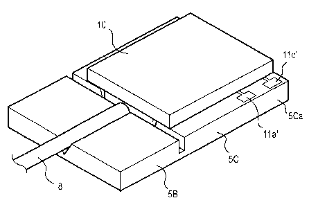
Next referring to Fig. 5B, a generally rectangular substrate 5,
which is greater both in width and length than the optical
waveguide substrate 105, is formed in its top surface with a dicing
groove 5e extending transversely of the length of the substrate 5 so
as to divide the length thereof into two sections to thereby define a
mount substrate section 5C and a V-grooved substrate section 5B.
CA 02278826 1999-09-15
-15-
As in the case of Fig. 3B, the V-grooved substrate section 5B has
formed therein a V groove 5c extending from the center of the end
face thereof into communication with the dicing groove 5e. The
mount substrate section 5C has formed in its top surface a recess 12
extending from the end face of the section opposite from the dicing
groove 5e into communication with the dicing groove 5e so as to
leave banks 5Ca, 5Cb on the opposite sides of the recess. The
width of the recess 12 is sized to accommodate the clad layer 3.
Formed on the top surfaces of the banks 5Ca, 5Cb are alignment
l0 marks 4a', 4b', 4c' and 4d' in correspondence with the alignment
marks 4a, 4b, 4c and 4d shown in Fig. 5A. Further formed on the
top surfaces of the banks 5Ca, 5Cb are H-shaped electrodes 11a',
11b', 11c' and 11d' having inner lands which will underlie the
substrate lOS and outer lands which will be positioned outside of
the substrate. The inner lands have solder bumps 13 formed
thereon. In assembly, the clad layer 3 and the laser diode 9 and
photo diode 15 protruding from the surface of the optical waveguide
substrate lOS are all accommodated in the recess 12.
After the laser diode 9 and photo diode 15 have been
mounted on the optical waveguide substrate lOS as described above
with reference to Fig. 5A, the resulting optical waveguide chip 10 is
turned upside down and placed in position on the mount substrate
section 5C described in Fig. 5B with reference to the alignment
marks 4a'- 4d' to form an assembly as shown in Fig. 6. Then, the
entire assembly is heated while the substrate 10S is pressed
against the mount substrate section 5C to bond them together by
means of the solder bumps 13. Further, gaps (recess 12) between
CA 02278826 1999-09-15
-16-
the optical waveguide chip 10 and the mount substrate section 5C is
filled with resin to protect the mounted laser diode 9 and photo
diode 15.
Referring now to Figs. 7A, 7B, 7C and Fig. 8, an optical
transmission/receiving module in still another embodiment of the
optical waveguide device according to this invention will be
described below.
In the art of optical communication, plans are now afoot to
provide both bi-directional digital communications via signal light
l0 with a wavelength of 1.31 ~,m and analog picture broadcasting via
signal light with a wavelength of 1.55 ~.m in a single optical fiber.
In this instance, a terminal equipment designed to utilize such
signal lights would need a bi-directional communication module
capable of separating the signal lights of two wavelengths of 1.31
~m and 1.55 ~,m through a filter prior to introducing the signal light
of 1.31 ~,m into both of the laser diode 9 and photo diode 15 while
introducing the signal light of 1.55 ~,m into a picture receiver (not
shown).
In the embodiment of Figs. 7A, 7B, 7C and Fig. 8, a single
2o silicon substrate 5 is divided into three regions, a central mount
substrate section 5C and two V-grooved substrate sections 5A, 5B
on the opposite sides of the mount substrate section 5C as in the
embodiment of Figs. 3A, 3B, 3C. The mount substrate section 5C
has formed by etching in its top surface a recess 12 extending from
the dicing groove 5d into communication with the dicing groove 5e
so as to define banks SCa, 5Cb on the opposite sides of the recess
like the embodiment of Fig. 5B. The V-grooved substrate section
CA 02278826 1999-09-15
-17-
5A is formed with a V groove 5a and may have formed on the top
surface thereof electrodes 11a, 11b on which optical-electronic
elements (such as laser diode 9 and photo diode 15) may be
mounted.
Now with reference to Fig. '7A, a clad layer 3 having an
optical waveguide 2 embedded therein is formed on an optical
waveguide substrate 105. The optical waveguide 2 in this
embodiment comprises a straight optical waveguide path 2D for
transmitting signal light of a wavelength of 1.31 ~,m and signal
l0 light of a wavelength of 1.55 ~.m and optical branch passages 2a, 2b,
2c constituting a Y-branched optical waveguide path 2Y for
transmitting signal light of a wavelength of 1.31 ~.m. The ends of
the straight optical waveguide path 2D and the optical branch
passage 2c are coupled together, the coupled end face lying in the
end surface 10b of the clad layer 3. Formed on the end surface lOb
of the clad layer 3 over the coupled end face is a dielectric multi-
layer film filter 14 allowing the passage of the signal light of a
wavelength of 1.31 ~m but reflecting the signal light of a
wavelength of 1.55 ~,m. It is seen in Fig. 7B which is a top plan
view of the optical waveguide chip 10 that the end surface lOb of the
clad layer 3 with which the coupled end face intersect is not at right
angles but at an angle with respect to the straight optical
waveguide path 2D so that the reflected light at the dielectric
multi-layer film filter 14 may be introduced into the optical branch
passage 2c. More specifically, the angle is chosen such that a line
bisecting the angle defined at the coupled end between the straight
optical waveguide path 2D and the optical branch passage 2c makes
CA 02278826 1999-09-15
-I8-
a right angle with the plane of the end surface lOb of the clad layer
3. The optical waveguide 2 and the alignment marks 4a, 4b may
be formed by the same method as that described with reference to
Figs. 4A-4G. It is to be noted that the fact that the optical
waveguide 2 is formed on the optical waveguide substrate lOS
separate from the device substrate 5 is a favorable factor in forming
the dielectric multi-layer film filter 14 the end surface of the optical
waveguide 2 and actually facilitates the formation of the filter.
Referring to Fig. 7C, the V-grooved substrate section 5A of
l0 the device substrate 5 is formed with a V groove 5a for receiving
and securing an optical fiber 8a intersecting at right angles with
the dicing groove 5d, and has formed on the top surface thereof
electrodes 11a and llb with which a photo diode 15 (Fig. 8) and a
laser diode 9 (Fig. 8) may be connected. The direction of extension
of the dicing groove 5e is angled at ~/2 with respect to a direction
perpendicular to the direction of extension of the V groove 5a such
that the direction of extension of the groove 5e will coincide with the
plane of the end surface lOb of the optical waveguide substrate 10S
when the optical waveguide chip 10 is turned upside down and
placed on the mount substrate section 5C. The V groove 5c is
formed in the V-grooved substrate section 5B to extend such that it
will coincide with the direction of extension of the V groove 5a.
The optical waveguide chip 10 shown in Fig. 7A is turned
upside down and placed in position on the mount substrate section
5C shown in Fig. 7C with the waveguide chip and the mount
substrate section being aligned with each other by superposing the
alignment marks 4a, 4b on the optical waveguide chip 10 over the
CA 02278826 1999-09-15
-19-
alignment marks 4a', 4b' on the mount substrate section 5C,
followed by bonding the optical waveguide chip 10 and the
substrate 5 together of form an integral assembly. In addition,
optical fibers 8a and 8c are fitted and fixed in the V grooves 5a and
5b, respectively to form an optical transmission/receiving module as
shown in Fig. 8.
In order to register the alignment marks 4a, 4b formed on
the optical waveguide chip 10 and the alignment marks 4a', 4b'
formed on the mount substrate section 5C while recognizing one
to against the other, a camera may be inserted between the opposed
substrates to perform the alignment procedures while
simultaneously observing the patterns of the opposed alignment
marks. Alternatively, light having a high penetrating power such
as infrared rays or X rays may be used to irradiate the alignment
marks on the substrates so that the alignment process may be
carried out by observing the transmitted light. The optical
waveguide substrate lOS and the device substrate 5, which have
actually extremely thin thickness on the order of 500 ~.m , permits
easy transmission of infrared rays or X rays to allow the operator to
2o fluoroscope the alignment marks. The positioning and alignment
process as described above not only is very simple and easy but also
requires only a short period time.
In the optical transmission/receiving module the assembly of
which has been completed, the optical fibers 8a and 8c have their
central axes in opposition to the centers of the end faces of the
straight optical waveguide path 2D while the laser diode 9 and
photo diode 15 are in opposition to the centers of the end faces of the
CA 02278826 1999-09-15
-20-
respective branch passages of the Y-branched optical waveguide
path 2Y
With the construction as described above in connection with
Figs. '7 and 8, signal light LS3 of a wavelength of 1.55 p,m
introduced through the optical fiber 8a on one side is passed into
the straight optical waveguide path 2D, penetrates through the
dielectric multi-layer film filter 14 and is output to the optical fiber
8c on the other side. In contrast, signal light LS 1 of a wavelength
of 1.31 ~,m introduced through the optical fiber 8a on one side is
to passed into the straight optical waveguide path 2D and reflected at
the dielectric rnulti-layer film filter 14 to be introduced into the Y-
branched optical waveguide path 2Y and is received by the photo
diode 15 positioned in opposition to the end face of the optical
branch passage 2a. Signal light LS2 of a wavelength of 1.31 ~.m
transmitted from the laser diode 9 is introduced into the optical
branch passage 2c through the end face of the optical branch
passage 2b opposing the laser diode 9, is reflected at the dielectric
multi-layer film filter 14 to be introduced into the straight optical
waveguide path 2D and is then output to the optical fiber 8a on the
one side. It will thus be appreciated that this invention allows for
both providing bi-directional digital communications via signal
light of a wavelength of 1.31 ~.m and by passing signal light of a
wavelength of 1.55 ~,m in a single optical fiber.
EFFECTS OF THE INVENTION
From the foregoing description, it can be seen that this
invention involves forming on a substrate of raw material an optical
CA 02278826 1999-09-15
-21-
waveguide embedded in a clad layer and alignment marks by
utilization of etching and film forming techniques to constitute an
optical waveguide chip, forming on a substrate of raw material V
grooves and alignment marks by utilization of etching and film
forming techniques to constitute a device substrate, whereby
positioning and securing of the optical waveguide chip and the
device substrate relative to each other may be effected easily and
accurately by referring to the alignment marks on the chip and the
substrate. In spite of the fact that the alignment operation
l0 according to this invention is based on the so-called passive
alignment technique, the accuracy in positioning and alignment is
comparable to that obtainable by the active alignment technique,
and yet the positioning and aligning process of this invention not
only is simple and easy, but also requires only a short period time.